The Role of Twistronics in Optical Modulation Technologies.
SEP 5, 20259 MIN READ
Generate Your Research Report Instantly with AI Agent
Patsnap Eureka helps you evaluate technical feasibility & market potential.
Twistronics Background and Optical Modulation Goals
Twistronics emerged as a groundbreaking field in condensed matter physics following the discovery of superconductivity in twisted bilayer graphene in 2018. This revolutionary approach involves manipulating the electronic properties of two-dimensional materials by adjusting the twist angle between stacked layers, creating moiré patterns that fundamentally alter material behavior. The field has rapidly evolved from theoretical concepts to experimental demonstrations, with researchers discovering that even slight angular adjustments can dramatically transform electrical, optical, and mechanical properties of layered materials.
The historical development of twistronics traces back to graphene research, but has expanded to include various 2D materials such as transition metal dichalcogenides (TMDs), hexagonal boron nitride (hBN), and their heterostructures. Each material combination offers unique properties and potential applications, particularly in the realm of optical modulation where precise control of light-matter interactions is essential.
Optical modulation technologies have simultaneously undergone significant advancement, transitioning from traditional electro-optic modulators to integrated photonic devices. Current optical modulators face persistent challenges in achieving high modulation speeds, low power consumption, and compact form factors—limitations that conventional materials struggle to overcome.
The convergence of twistronics with optical modulation represents a promising frontier with several key objectives. Primary among these is developing tunable optical modulators that leverage the angle-dependent properties of twisted 2D materials to achieve unprecedented control over light propagation, absorption, and emission. Researchers aim to create devices capable of ultra-fast modulation speeds reaching terahertz frequencies while maintaining nanoscale dimensions.
Another critical goal involves establishing reliable fabrication techniques for precisely controlling twist angles in large-area devices, essential for commercial viability. The field also seeks to develop comprehensive theoretical models that accurately predict optical behavior in twisted heterostructures, enabling rational design of next-generation devices.
The potential applications span multiple industries, from telecommunications requiring high-bandwidth optical interconnects to quantum information processing where precise control of photon states is paramount. Additionally, researchers envision advanced sensing platforms and novel display technologies leveraging the unique optical properties of twisted materials.
As the field progresses, interdisciplinary collaboration between materials scientists, photonics engineers, and quantum physicists will be essential to overcome current technical barriers and fully realize the transformative potential of twistronics in optical modulation technologies.
Market Analysis for Twistronics-Based Optical Modulators
The global market for twistronics-based optical modulators is experiencing significant growth potential, driven by increasing demand for high-speed data transmission and advanced photonic integrated circuits. Current market projections indicate that the photonic integrated circuit market, which encompasses optical modulators, is expected to reach $3.2 billion by 2027, with twistronics-based solutions positioned to capture an emerging segment within this space.
The telecommunications sector represents the largest potential market for twistronics-based optical modulators, particularly in 5G and upcoming 6G infrastructure deployments where high-bandwidth, energy-efficient signal processing is critical. Telecommunications companies are actively seeking solutions that can overcome the bandwidth limitations of conventional electro-optic modulators while reducing power consumption.
Data center operators constitute another significant market segment, as they face mounting pressure to increase data transmission speeds while minimizing energy consumption. The ability of twistronics-based modulators to achieve higher modulation speeds with lower power requirements directly addresses these pain points, potentially offering substantial operational cost savings in large-scale implementations.
The defense and aerospace sectors are showing strategic interest in twistronics technology for secure communications and advanced sensing applications. These sectors value the potential for compact, lightweight, and radiation-resistant optical components that can operate reliably in harsh environments.
Consumer electronics represents a longer-term market opportunity, particularly as augmented reality (AR) and virtual reality (VR) systems evolve to require more sophisticated optical components. Industry analysts project that AR/VR markets could create demand for advanced optical modulators worth $500 million annually by 2030.
Regional analysis reveals that North America currently leads in research and development investments for twistronics-based photonics, with major universities and corporate research centers concentrated in the United States. Asia-Pacific, particularly China, South Korea, and Japan, is rapidly expanding its capabilities in this domain, supported by substantial government funding initiatives for next-generation communication technologies.
Market adoption faces several challenges, including high initial manufacturing costs, scalability concerns, and competition from established technologies like lithium niobate modulators. However, the performance advantages of twistronics-based solutions—particularly in terms of modulation bandwidth, energy efficiency, and form factor—create compelling value propositions for specific high-performance applications.
Industry partnerships between academic institutions, material science companies, and telecommunications equipment manufacturers are accelerating commercialization efforts. These collaborations are essential for translating laboratory breakthroughs into manufacturable products that meet industry standards and reliability requirements.
Current Challenges in Twistronics for Optical Applications
Despite significant advancements in twistronics for optical modulation, several critical challenges impede its full implementation in practical optical applications. The primary obstacle remains the precise control of twist angles between 2D material layers. Even minor deviations of 0.1 degrees can dramatically alter the moiré superlattice structure, resulting in unpredictable optical properties. This precision requirement presents formidable manufacturing hurdles, particularly when scaling beyond laboratory demonstrations.
Temperature sensitivity constitutes another significant challenge. The optical properties of twisted bilayer systems exhibit substantial variations with temperature fluctuations, complicating their integration into devices that must operate across diverse environmental conditions. This thermal instability necessitates sophisticated temperature control mechanisms, adding complexity and cost to potential commercial applications.
The interface quality between twisted layers critically affects optical performance. Current fabrication techniques struggle to eliminate contaminants, bubbles, and wrinkles at these interfaces, which introduce scattering centers and degrade optical modulation efficiency. These imperfections become particularly problematic when attempting to achieve uniform optical responses across larger areas.
Stability and degradation issues also plague twistronics-based optical systems. Exposure to ambient conditions, including oxygen and moisture, can significantly alter the electronic and optical properties of 2D materials. The encapsulation technologies required to protect these delicate structures often introduce additional optical interfaces that may compromise device performance.
Integration challenges with conventional photonic platforms represent another substantial hurdle. The atomically thin nature of twisted 2D materials makes coupling with standard optical waveguides and fibers inefficient. The mode mismatch between traditional photonic components and twistronics-based modulators results in significant insertion losses that diminish overall system performance.
The reproducibility of optical characteristics across multiple devices remains inconsistent, hampering commercial viability. Current fabrication processes yield considerable device-to-device variations, making standardized production challenging. This variability stems from both the inherent sensitivity of twistronics to structural parameters and limitations in current manufacturing precision.
Finally, theoretical understanding of the complex light-matter interactions in twisted systems remains incomplete. While the electronic properties of twisted bilayers have been extensively studied, their optical response mechanisms—particularly under dynamic modulation conditions—require further fundamental research to enable optimized device designs and performance predictions.
Existing Twistronics-Based Optical Modulation Solutions
01 Twistronics-based optical modulators
Optical modulators based on twistronics principles utilize the manipulation of twisted layers of 2D materials to control light properties. These devices leverage the unique electronic and optical properties that emerge when layers are stacked at specific twist angles, enabling precise modulation of optical signals. The technology allows for tunable optical properties through electrical control of the twist angle, offering high-speed modulation capabilities for advanced photonic applications.- Twistronics-based optical modulators: Optical modulators based on twistronics principles utilize the manipulation of twisted layers of 2D materials to control light properties. These devices leverage the unique electronic and optical properties that emerge when layers are stacked at specific twist angles, enabling precise modulation of optical signals. The technology allows for efficient control of light transmission, phase, and polarization through tunable interlayer coupling.
- Integrated photonic devices with twisted materials: Integration of twistronics principles into photonic circuits enables advanced optical signal processing capabilities. These integrated devices combine twisted 2D material structures with conventional photonic components to achieve enhanced functionality. The integration allows for compact optical modulators with high bandwidth and low power consumption, suitable for next-generation optical communication systems.
- Electro-optic modulation techniques: Electro-optic modulation techniques in twistronics involve applying electric fields to twisted material interfaces to control optical properties. These methods enable rapid switching and precise control of light transmission through the manipulation of the electronic structure at the twisted interfaces. The approach offers advantages in modulation speed and efficiency compared to conventional optical modulation technologies.
- Waveguide-based optical modulation systems: Waveguide structures incorporating twisted 2D materials enable efficient optical modulation in compact form factors. These systems guide light through channels where twistronics effects can be maximized to achieve strong light-matter interactions. The waveguide architecture allows for enhanced modulation depth and bandwidth while maintaining compatibility with existing photonic platforms.
- Tunable optical properties through angle control: Precise control of the twist angle between stacked 2D material layers enables tunable optical properties for modulation applications. By adjusting the relative orientation of layers, the electronic band structure can be modified, directly affecting light absorption, transmission, and phase characteristics. This tunability allows for reconfigurable optical modulators that can be optimized for different wavelengths and modulation requirements.
02 Integrated photonic devices with twistable structures
Integration of twistronics principles into photonic circuits enables novel functionalities in optical communication systems. These integrated devices combine twisted 2D material structures with conventional photonic components to achieve enhanced modulation efficiency and bandwidth. The integration allows for compact device footprints while maintaining high performance in signal processing and transmission applications, particularly in high-speed optical networks.Expand Specific Solutions03 Moiré pattern-based optical modulation techniques
Optical modulation techniques utilizing moiré patterns formed by twisted layers enable precise control over light propagation and manipulation. These techniques exploit the periodic potential created by the moiré superlattice to modulate optical properties such as refractive index and absorption. The approach offers advantages in terms of modulation depth and wavelength selectivity, making it suitable for applications in optical filtering, sensing, and signal processing.Expand Specific Solutions04 Electro-optic effects in twisted van der Waals heterostructures
Twisted van der Waals heterostructures exhibit enhanced electro-optic effects that can be harnessed for optical modulation. By applying electric fields to these structures, significant changes in optical properties can be induced due to the modified electronic band structure at specific twist angles. This approach enables voltage-controlled optical modulation with high efficiency and fast response times, suitable for applications in telecommunications and optical computing.Expand Specific Solutions05 Waveguide-based implementation of twistronics optical modulators
Waveguide architectures incorporating twistronics principles provide an effective platform for optical signal modulation. These implementations integrate twisted 2D material structures with optical waveguides to achieve efficient light-matter interaction and modulation. The waveguide geometry enhances the interaction length between light and the active twistronics medium, resulting in improved modulation efficiency and reduced power consumption for optical signal processing applications.Expand Specific Solutions
Key Industry Players in Twistronics Research
Twistronics in optical modulation technologies is emerging as a transformative field, currently in its early development stage with significant growth potential. The market is expanding rapidly as companies recognize the advantages of manipulating twisted van der Waals heterostructures for enhanced optical properties. While still evolving toward commercial maturity, key players are making substantial advances. Research institutions like MIT and Caltech are pioneering fundamental discoveries, while technology giants including Fujitsu, NEC, Intel, and Huawei are developing practical applications. Electronics specialists such as Sumitomo Osaka Cement, Seiko Epson, and Samsung Electro-Mechanics are exploring integration possibilities, with semiconductor manufacturers like GlobalFoundries and ASML providing essential fabrication capabilities. This competitive landscape reflects a technology transitioning from research to commercial implementation.
NTT, Inc.
Technical Solution: NTT在扭曲电子学光调制技术领域开发了独特的"IOWN"(Innovative Optical and Wireless Network)架构的关键组件。其技术方案基于扭曲二维材料的光电特性,特别是利用过渡金属二硫化物(TMDs)如MoS₂和WS₂的层间扭转效应。NTT研究团队创新性地将扭曲角度精确控制在3-5°范围内,在这一"次魔角"区域发现了独特的光学调制效应,可实现超低功耗的光信号处理。NTT的光调制器采用了独特的叠层结构,将扭曲TMDs与光波导紧密集成,通过电场调控扭曲层间的电子态分布,进而改变材料的复折射率。这种方法实现了超过40dB的消光比和小于1pJ/bit的能耗,同时保持了10GHz以上的调制带宽。NTT还开发了专用的封装技术,解决了扭曲二维材料器件的稳定性和可靠性问题,使其能够在实际通信网络环境中长期稳定工作。该技术已在NTT的实验网络中进行了现场测试,展示了在下一代全光网络中的应用潜力。
优势:在光通信领域拥有深厚的技术积累和市场影响力;研发了专用的扭曲角度控制工艺,提高了器件一致性;在器件封装和可靠性方面有独特技术;已建立了从实验室到现场测试的完整验证链。劣势:器件成本较高,难以在短期内实现大规模商业化;在某些应用场景下,调制速度不如传统技术;技术路线较为独特,与主流光通信设备的兼容性需要进一步验证。
California Institute of Technology
Technical Solution: Caltech在扭曲电子学光调制技术领域处于领先地位,开发了基于莫尔超晶格(moiré superlattices)的新型光调制器。其研究团队利用双层石墨烯之间的扭转角度控制来实现可调谐的光学特性,创造出具有精确角度依赖性的光电器件。他们的技术方案包括在双层二维材料之间引入特定扭转角度(通常在1.1°左右,即"魔角"),利用由此产生的电子态密度变化来调控光的吸收和发射特性。这种方法能够在近红外到太赫兹波段实现超快光调制,响应时间可达飞秒级别,且能耗显著低于传统电光调制器。Caltech还开发了集成化工艺,将扭曲电子学器件与硅基光子学平台兼容,为下一代光通信和量子信息处理提供了新途径。
优势:在基础研究方面处于绝对领先地位,拥有多项扭曲电子学基础专利;实验室演示的器件具有超高调制速度和极低能耗;研究成果发表在Nature和Science等顶级期刊。劣势:技术成熟度较低,距离商业化应用仍有距离;大规模制造工艺尚未完全解决;器件稳定性和一致性需要进一步提高。
Critical Patents and Research in Twistronics Modulation
Optical device including optical modulation device, and driving method thereof
PatentActiveUS10354576B2
Innovation
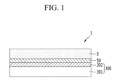
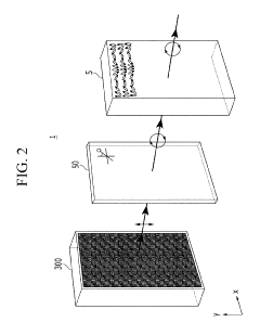
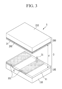
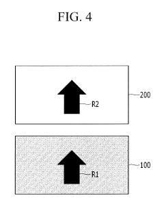
- An optical device with an optical modulation device comprising a liquid crystal layer between two plates, where the liquid crystal molecules are controlled through in-plane rotation by applying specific driving signals to electrodes, allowing for continuous phase modulation by tilting parallel or perpendicular to the plates' surfaces, enabling the device to function as a lens or prism.
Twistable electronic device module
PatentActiveTW202249554A
Innovation
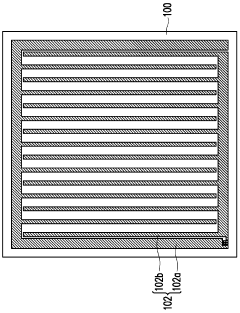
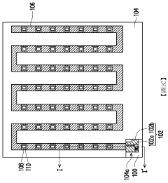
- A twistable electronic component module with a twistable substrate, electrode pattern layer, insulating layer, circuit layer, and circuit boards, where circuit boards are arranged between electronic components and the circuit layer, minimizing direct contact and potential damage.
Material Science Advancements for Twisted 2D Structures
Recent advancements in material science have revolutionized the field of twistronics, particularly in the development of twisted 2D structures. The discovery that rotating layers of 2D materials at specific "magic angles" can dramatically alter their electronic properties has opened new frontiers in optical modulation technologies. Graphene bilayers twisted at approximately 1.1 degrees have demonstrated superconductivity and other exotic quantum states, providing unprecedented opportunities for manipulating light-matter interactions.
The fabrication techniques for twisted 2D structures have evolved significantly in recent years. Precision methods such as tear-and-stack, mechanical assembly with angular control, and chemical vapor deposition with controlled growth parameters now enable the creation of high-quality twisted heterostructures with angular precision approaching 0.1 degrees. These techniques have been crucial in overcoming previous limitations in creating consistent and scalable twisted material systems.
Material combinations beyond graphene-graphene interfaces have expanded the toolkit for optical modulation. Transition metal dichalcogenides (TMDs) such as MoS2, WS2, and WSe2 in twisted configurations exhibit unique moiré potentials that create localized exciton states with distinctive optical signatures. Heterostructures combining different 2D materials (such as graphene-hBN or MoS2-WS2) introduce additional degrees of freedom for engineering band structures and optical properties.
The physical properties of twisted 2D structures directly relevant to optical modulation include moiré-induced band structure modifications, interlayer exciton formation with extended lifetimes, and enhanced light-matter coupling. These properties enable novel electro-optic effects with switching speeds potentially reaching terahertz frequencies and modulation depths exceeding conventional materials by orders of magnitude.
Characterization techniques have also advanced to meet the challenges of studying these complex structures. High-resolution transmission electron microscopy (HR-TEM) now allows direct visualization of moiré patterns, while angle-resolved photoemission spectroscopy (ARPES) provides detailed band structure information. Optical techniques such as second harmonic generation microscopy offer non-destructive methods to map twist angles across samples with sub-micron resolution.
The stability and reliability of twisted 2D structures remain challenging, with environmental sensitivity and structural relaxation effects requiring innovative encapsulation strategies. Recent developments in hexagonal boron nitride (hBN) encapsulation have significantly improved device lifetimes, while new theoretical models are helping to predict and mitigate relaxation effects that can disrupt the desired twist angles over time.
Integration Challenges with Conventional Photonics
The integration of twistronics-based optical modulation technologies with conventional photonic systems presents significant challenges that must be addressed for practical implementation. The fundamental mismatch between the atomic-scale nature of twisted van der Waals heterostructures and traditional photonic components creates substantial interface difficulties. Conventional silicon photonics typically operate at micrometer scales, while twistronics effects manifest at nanometer scales, creating a dimensional incompatibility that complicates direct integration.
Signal conversion and preservation represent another critical challenge. The unique quantum properties that make twistronics attractive for optical modulation can be easily disrupted during integration with conventional waveguides and photonic circuits. Maintaining coherence across these different technological domains requires sophisticated interface engineering that has not yet been fully developed.
Fabrication compatibility issues further complicate integration efforts. Twistronics devices require precise atomic alignment and clean interfaces between 2D material layers, achieved through specialized fabrication techniques. These methods often conflict with standard CMOS-compatible processes used in conventional photonics manufacturing. The temperature sensitivities and material compatibility constraints between these fabrication approaches create significant production hurdles.
Scalability remains perhaps the most pressing concern for commercial viability. While laboratory demonstrations have shown promising results for individual twistronics-based modulators, scaling these devices to integrated photonic circuits containing thousands of components presents unresolved challenges. Current fabrication techniques for precisely twisted heterostructures are largely artisanal and not amenable to mass production methodologies.
The thermal management of integrated twistronics-photonic systems presents additional complications. Many twistronics effects are highly temperature-sensitive, with optimal performance occurring at specific temperature ranges. Conventional photonic circuits generate heat during operation, potentially disrupting the delicate twist angles and interlayer coupling that enable the desired optical modulation properties.
Addressing these integration challenges requires interdisciplinary approaches combining expertise from materials science, nanofabrication, photonic engineering, and quantum electronics. Recent research has begun exploring intermediate interface layers and hybrid integration strategies that could bridge the gap between twistronics and conventional photonics. These include the development of specialized coupling structures and buffer layers designed to preserve the quantum properties of twisted materials while enabling efficient optical signal transfer to conventional photonic waveguides.
Unlock deeper insights with Patsnap Eureka Quick Research — get a full tech report to explore trends and direct your research. Try now!
Generate Your Research Report Instantly with AI Agent
Supercharge your innovation with Patsnap Eureka AI Agent Platform!
