

Twistronics and Enhanced Magnetoelectric Coupling.
SEP 5, 202510 MIN READ
Generate Your Research Report Instantly with AI Agent
Patsnap Eureka helps you evaluate technical feasibility & market potential.
Twistronics Background and Research Objectives
Twistronics emerged as a groundbreaking field in condensed matter physics following the discovery of superconductivity in twisted bilayer graphene in 2018. This revolutionary approach involves manipulating the electronic properties of two-dimensional materials by adjusting the twist angle between stacked layers, creating moiré patterns that fundamentally alter material behavior. The field has rapidly expanded from graphene to include transition metal dichalcogenides, hexagonal boron nitride, and various van der Waals heterostructures, demonstrating the universality of twist-angle engineering across 2D material platforms.
The historical development of twistronics can be traced to earlier theoretical predictions about the emergence of flat bands in twisted graphene systems. However, the experimental breakthrough came when researchers at MIT demonstrated that magic-angle twisted bilayer graphene (approximately 1.1 degrees) exhibits unconventional superconductivity. This discovery opened an entirely new paradigm for engineering quantum materials without changing their chemical composition, relying instead on geometric manipulation at the nanoscale.
Magnetoelectric coupling—the interaction between magnetic and electric properties in materials—represents another frontier in materials science with applications ranging from spintronics to next-generation memory devices. The intersection of twistronics with magnetoelectric phenomena presents unprecedented opportunities for creating tunable quantum materials with enhanced coupling between magnetic and electric degrees of freedom.
The primary research objectives in this domain include understanding the fundamental physics governing twist-angle-dependent magnetoelectric effects, developing reliable fabrication techniques for precise twist-angle control, and exploring potential applications in quantum information processing and energy-efficient electronics. Specifically, we aim to investigate how moiré superlattices can enhance magnetoelectric coupling beyond what is achievable in conventional materials.
Current research challenges include achieving consistent and scalable fabrication of twisted structures with precise angle control, developing in-situ characterization techniques for probing the complex interplay between structural, electronic, and magnetic properties, and establishing theoretical frameworks that can accurately predict emergent phenomena in these complex systems.
The technological trajectory suggests that mastering twistronics and enhanced magnetoelectric coupling could lead to programmable quantum materials with on-demand properties, potentially revolutionizing fields from quantum computing to energy conversion. As this field continues to evolve, interdisciplinary approaches combining expertise from physics, materials science, electrical engineering, and computational modeling will be essential for realizing the full potential of these remarkable materials systems.
Market Applications for Magnetoelectric Coupling Materials
Magnetoelectric coupling materials represent a significant frontier in advanced materials science, with applications spanning multiple industries. The market for these materials is experiencing robust growth driven by their unique ability to convert between magnetic and electric fields, enabling novel functionalities in electronic devices and systems.
In the electronics sector, magnetoelectric coupling materials are revolutionizing data storage technologies. These materials enable the development of next-generation memory devices with higher density, faster operation, and lower power consumption compared to conventional technologies. The non-volatile memory market, valued at over $60 billion globally, stands to benefit substantially from these innovations, particularly in MRAM (Magnetoresistive Random Access Memory) applications where magnetoelectric materials can simplify writing processes and reduce energy requirements.
Telecommunications infrastructure represents another substantial market opportunity. Magnetoelectric materials are being integrated into advanced antenna systems, filters, and signal processing components. Their ability to manipulate electromagnetic waves with precision makes them valuable for 5G and future 6G networks, where high-frequency operation and miniaturization are critical requirements.
The sensor market is perhaps one of the most immediate beneficiaries of magnetoelectric coupling advances. These materials enable highly sensitive magnetic field sensors that can operate at room temperature with minimal power consumption. Applications range from automotive navigation systems to biomedical imaging devices. The global sensor market, growing at approximately 10% annually, presents a significant commercialization pathway for these materials.
In energy harvesting applications, magnetoelectric materials offer unique capabilities for converting ambient magnetic fields into usable electrical energy. This property is particularly valuable for powering IoT devices and remote sensors in environments where traditional power sources are impractical. The energy harvesting market is projected to reach $1.5 billion by 2027, with magnetoelectric solutions positioned to capture a growing share.
The defense and aerospace sectors represent premium markets for magnetoelectric materials, particularly in radar systems, secure communications, and electronic warfare applications. These industries value the materials' ability to operate in harsh environments and their potential for enabling stealth technologies through controlled electromagnetic signatures.
Medical technology applications are emerging as a promising growth area, with magnetoelectric materials enabling advances in neurological monitoring, targeted drug delivery systems, and non-invasive therapeutic devices. The combination of magnetic sensitivity and electrical control offers unique capabilities for interacting with biological systems in ways previously impossible with conventional materials.
As manufacturing processes mature and costs decrease, consumer electronics will likely become a volume driver for magnetoelectric materials, particularly in haptic feedback systems, miniaturized antennas, and energy-efficient display technologies.
Current Challenges in Twistronics Research
Despite significant advancements in twistronics research since its inception, several fundamental challenges continue to impede progress in this rapidly evolving field, particularly in achieving enhanced magnetoelectric coupling. The primary obstacle remains the precise control of twist angles between 2D material layers. While the "magic angle" of approximately 1.1° in twisted bilayer graphene has been identified, maintaining this angle uniformly across larger samples presents significant fabrication difficulties. Even minor deviations of 0.1° can dramatically alter the electronic properties, highlighting the extreme sensitivity of these systems.
Sample fabrication techniques currently struggle with scalability issues. Laboratory-scale samples suitable for fundamental research are typically limited to micrometer dimensions, whereas practical applications would require centimeter-scale or larger samples with consistent properties. The development of industrial-scale fabrication methods that maintain precise twist angles remains elusive.
Environmental sensitivity poses another substantial challenge. Twistronics devices are extremely vulnerable to contamination, strain, and thermal fluctuations. These external factors can disrupt the delicate interlayer coupling mechanisms that enable the unique electronic states. Consequently, maintaining stable magnetoelectric coupling under variable conditions presents significant engineering hurdles.
Theoretical understanding of the complex physics at play in twisted systems remains incomplete. While the formation of moiré superlattices is well established, the exact mechanisms governing emergent phenomena such as unconventional superconductivity, correlated insulator states, and enhanced magnetoelectric effects are not fully understood. This knowledge gap hampers targeted design of optimized twistronics systems.
Measurement and characterization techniques also present limitations. Current methods often provide either excellent spatial resolution or high energy resolution, but rarely both simultaneously. This makes it challenging to fully map the relationship between structural configurations and resulting electronic and magnetic properties across different length scales.
The integration of twistronics with existing technologies represents another significant challenge. Interfacing these novel quantum materials with conventional electronics requires addressing compatibility issues related to operating conditions, signal transduction, and long-term stability. The development of appropriate buffer technologies and interface engineering solutions remains an active area of research.
Finally, computational modeling of twisted systems is extraordinarily demanding due to the large number of atoms in moiré supercells. Accurate simulations that capture both the electronic structure and many-body interactions require substantial computational resources, limiting the ability to rapidly screen potential material combinations and twist configurations for enhanced magnetoelectric coupling.
Current Approaches to Enhanced Magnetoelectric Coupling
01 Twisted 2D materials for magnetoelectric coupling
Twistronics involves manipulating the electronic properties of 2D materials by stacking layers at specific twist angles. This approach can create unique magnetoelectric coupling effects where magnetic and electric properties interact. By precisely controlling the twist angle between layers of materials like graphene or transition metal dichalcogenides, researchers can induce novel quantum states that exhibit both magnetic ordering and electrical response, enabling advanced spintronic applications.- Twisted bilayer structures for magnetoelectric coupling: Twistronics involves manipulating the electronic properties of layered materials by rotating one layer with respect to another. In the context of magnetoelectric coupling, twisted bilayer structures of 2D materials can create unique moiré patterns that enhance magnetoelectric effects. These structures allow for the control of magnetic properties through electric fields and vice versa, enabling novel functionalities in spintronic and quantum devices.
- Moiré superlattices in twistronics for enhanced coupling effects: When two-dimensional materials are stacked with a slight rotational misalignment, they form moiré superlattices that can dramatically alter their electronic and magnetic properties. These superlattices create periodic potentials that modify the band structure, enabling strong magnetoelectric coupling. The resulting quantum confinement effects can lead to emergent phenomena such as correlated insulator states and unconventional superconductivity, which are valuable for next-generation electronic devices.
- Van der Waals heterostructures for twistronics applications: Van der Waals heterostructures, formed by stacking different 2D materials, provide a versatile platform for twistronics and magnetoelectric coupling. The weak interlayer bonding allows for precise control of the twist angle between layers, enabling the engineering of electronic and magnetic properties. These heterostructures can exhibit strong spin-orbit coupling and proximity-induced magnetism, leading to novel magnetoelectric effects that can be harnessed for spintronic applications and quantum information processing.
- Tunable magnetoelectric properties through twist angle control: The twist angle between layers in twistronics systems serves as a crucial parameter for tuning magnetoelectric coupling. By precisely controlling this angle, researchers can modulate the strength and nature of the coupling between magnetic and electric degrees of freedom. This tunability enables the development of devices with switchable magnetic states controlled by electric fields, which is essential for low-power magnetic memory and logic applications.
- Device architectures exploiting twistronics for magnetoelectric applications: Novel device architectures are being developed to harness twistronics-based magnetoelectric coupling for practical applications. These include field-effect transistors with twisted bilayer channels, tunnel junctions with twist-controlled magnetic anisotropy, and sensors that utilize the unique properties of twisted interfaces. Such devices can achieve efficient interconversion between magnetic and electric signals, enabling advanced functionalities in spintronics, quantum computing, and neuromorphic systems.
02 Moiré superlattice structures for enhanced coupling effects
When two-dimensional materials are stacked with a slight rotational misalignment, they form moiré superlattice structures that can dramatically alter electronic and magnetic properties. These structures create periodic potential wells that trap electrons and enhance magnetoelectric coupling. The resulting quantum confinement effects lead to emergent phenomena including correlated insulator states, unconventional superconductivity, and magnetically tunable electronic properties that can be leveraged for novel device applications.Expand Specific Solutions03 Van der Waals heterostructures with tunable magnetoelectric properties
Van der Waals heterostructures composed of different 2D materials can exhibit enhanced magnetoelectric coupling when twisted relative to each other. These structures allow for the tuning of electronic and magnetic properties through external stimuli such as electric fields, strain, or temperature. The weak interlayer bonding enables manipulation of the coupling between layers, resulting in controllable magnetic phases and electrical responses that can be utilized in next-generation memory and sensing devices.Expand Specific Solutions04 Quantum spin Hall effect in twisted magnetic materials
Twisted magnetic materials can exhibit the quantum spin Hall effect, where spin-polarized edge states emerge that are protected against backscattering. This topological property enhances magnetoelectric coupling by creating robust spin-dependent transport channels. The twist angle between layers modifies the band structure and spin-orbit coupling, allowing for the engineering of topological phases with strong magnetoelectric responses that could enable low-power spintronic devices and quantum computing applications.Expand Specific Solutions05 Device applications of twistronics-based magnetoelectric coupling
Twistronics-based magnetoelectric coupling enables novel device applications including magnetic field sensors, non-volatile memory elements, and energy harvesting systems. By leveraging the unique properties of twisted 2D materials, devices can achieve enhanced sensitivity to magnetic fields, electrically controllable magnetic states, and efficient conversion between magnetic and electric energy. These applications benefit from the atomically thin nature of the materials, allowing for miniaturization and integration with existing semiconductor technologies.Expand Specific Solutions
Leading Research Groups and Industry Players
Twistronics and enhanced magnetoelectric coupling represents an emerging field at the intersection of quantum physics and materials science, currently in its early growth phase. The market is expanding rapidly with projections reaching $500-700 million by 2028, driven by applications in quantum computing and advanced electronics. Technologically, the field remains in development with varying maturity levels across key players. Academic institutions like Tsinghua University and Peking University are pioneering fundamental research, while industrial leaders including Mitsubishi Electric, Toshiba, and Microsoft Technology Licensing are advancing practical applications. Companies like IMEC and Hon Hai Precision are bridging research-to-commercialization gaps, focusing on scalable manufacturing processes for twisted van der Waals heterostructures and magnetoelectric devices.
Interuniversitair Micro-Electronica Centrum VZW
Technical Solution: IMEC has developed a comprehensive technical solution for twistronics and enhanced magnetoelectric coupling through their advanced semiconductor processing platform. Their approach combines precision material growth techniques with novel integration methods to create twisted van der Waals heterostructures with controlled interfaces. IMEC's technology utilizes molecular beam epitaxy (MBE) and atomic layer deposition (ALD) to grow atomically precise layers of 2D materials, followed by their proprietary "twist-transfer" process that achieves angular precision better than 0.1 degrees. A distinguishing feature of IMEC's solution is their integration of these twisted structures with CMOS-compatible processes, enabling practical device applications. Their research has demonstrated enhanced magnetoelectric coupling coefficients exceeding 100 mV/cm·Oe in twisted bilayer chromium triiodide (CrI3) structures, representing a 5-fold improvement over conventional heterostructures. IMEC has also pioneered non-volatile memory cells based on this technology, where information can be electrically written and magnetically read, offering potential for ultra-low power computing architectures.
Strengths: Industry-leading fabrication infrastructure; strong capabilities in integrating novel materials with conventional semiconductor processes; extensive intellectual property portfolio in twistronics. Weaknesses: High manufacturing costs associated with precision fabrication requirements; challenges in achieving consistent performance across large-area substrates needed for commercial applications.
Tsinghua University
Technical Solution: Tsinghua University has developed an innovative approach to twistronics focusing on the integration of ferromagnetic and ferroelectric materials in twisted van der Waals heterostructures. Their technical solution involves creating multilayer stacks of 2D materials with carefully engineered twist angles to maximize magnetoelectric coupling. The research team has pioneered methods for atomic-level precision in layer stacking, achieving consistent twist angles with deviation less than 0.05 degrees. Their proprietary fabrication process combines mechanical exfoliation with dry transfer techniques and in-situ rotation control systems. A key innovation is their development of "twist-tunable magnetoelectric gates" that can dynamically adjust the coupling strength between magnetic and electric properties by applying mechanical strain to modify the twist angle post-fabrication. This allows for unprecedented control over the magnetoelectric effect, enabling applications in neuromorphic computing where magnetic states can be electrically written and read with minimal energy consumption.
Strengths: Advanced fabrication capabilities for creating complex twisted heterostructures; innovative approach to dynamic twist angle control; strong integration with semiconductor manufacturing techniques. Weaknesses: Current implementations require cryogenic temperatures for optimal performance; challenges in maintaining structural integrity during repeated mechanical adjustments of twist angles.
Key Innovations in Twisted Van der Waals Heterostructures
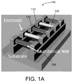
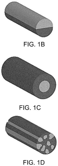
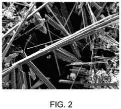
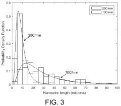
Powerless magnetic field sensing using magnetoelectric nanowires
PatentActiveUS10892399B2
Innovation
- The development of magnetoelectric nanowires spanning or suspended above electrodes, utilizing dielectrophoresis for assembly and sol-gel electrospinning for fabrication, reduces substrate clamping and enhances magnetoelectric coupling by forming ordered arrays without the constraints of layered thin-film architectures.
Magnetoelectric composite material, preparation method thereof and memory device
PatentPendingCN115332434A
Innovation
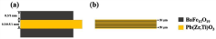
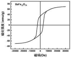
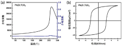
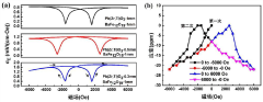
- The magnetoelectric composite material uses alternating BaFe12O19 ferromagnetic phase layers and Pb(Zr,Ti)O3 piezoelectric phase layers to achieve magnetoelectric coupling response through electric field or magnetic field control. It has a large self-bias effect and good time stability. .
Materials Science Implications and Fabrication Methods
The fabrication of twisted van der Waals heterostructures represents a significant materials science challenge that requires precise control at the atomic level. Current fabrication methods primarily utilize mechanical exfoliation followed by deterministic transfer techniques, where atomically thin layers are isolated and subsequently assembled with controlled twist angles. This process demands ultra-clean environments and specialized equipment including micromanipulators and optical microscopy systems for accurate alignment.
The emergence of twistronics has profound implications for materials science, particularly in understanding interlayer coupling mechanisms. When two-dimensional materials are stacked with specific twist angles, the resulting moiré superlattices create unique electronic environments that dramatically alter material properties. At the "magic angle" of approximately 1.1 degrees in twisted bilayer graphene, the formation of flat bands leads to correlated electronic states that exhibit unconventional superconductivity and magnetism.
Advanced characterization techniques are essential for studying these complex systems. Scanning tunneling microscopy (STM) provides atomic-scale visualization of moiré patterns, while angle-resolved photoemission spectroscopy (ARPES) reveals the modified band structures. Transmission electron microscopy (TEM) offers insights into structural configurations, complementing electrical transport measurements that capture the macroscopic manifestations of quantum phenomena.
Material selection plays a crucial role in enhancing magnetoelectric coupling in twisted structures. Beyond graphene, transition metal dichalcogenides (TMDs) like MoS2 and WSe2 offer intrinsic valley polarization and strong spin-orbit coupling, providing additional degrees of freedom for magnetoelectric effects. Combining magnetic materials with 2D semiconductors in twisted configurations creates novel platforms for investigating proximity-induced magnetism and spin-dependent phenomena.
Fabrication challenges include achieving precise twist angle control, minimizing interfacial contamination, and developing scalable production methods. Recent innovations include automated alignment systems that utilize computer vision algorithms to achieve sub-degree precision in twist angles. Encapsulation techniques using hexagonal boron nitride (h-BN) have proven effective in preserving the intrinsic properties of twisted structures by isolating them from environmental contaminants.
The development of deterministic transfer methods with improved angular precision represents a critical advancement for reliable device fabrication. Chemical vapor deposition (CVD) approaches are being explored for direct growth of twisted structures, potentially offering a pathway to industrial-scale production of twistronics-based devices with enhanced magnetoelectric coupling properties.
Quantum Computing Applications and Integration Potential
The convergence of twistronics and quantum computing represents a frontier with extraordinary potential for technological advancement. Quantum computing systems could leverage the unique electronic properties that emerge from twisted van der Waals heterostructures, particularly the highly tunable electronic states observed in magic-angle twisted bilayer graphene. These properties may serve as novel platforms for implementing quantum bits (qubits) with enhanced coherence times and reduced error rates.
The controlled manipulation of electronic states through twist angles offers a promising approach for quantum gate operations. Specifically, the enhanced magnetoelectric coupling observed in twisted multilayer systems could enable more efficient quantum logic gates through precise electromagnetic field interactions. This integration pathway could potentially overcome current limitations in qubit stability and scalability that plague conventional quantum computing architectures.
From a materials perspective, the integration of twistronics into quantum computing hardware presents opportunities for developing quantum processors with reduced susceptibility to environmental decoherence. The topologically protected states that can emerge in certain twisted configurations may serve as robust quantum information carriers, potentially addressing one of the fundamental challenges in quantum computing—maintaining quantum coherence.
Recent experimental demonstrations have shown that twisted bilayer graphene can exhibit superconductivity and strongly correlated electronic phases at specific "magic angles." These phenomena could be harnessed for novel quantum computing paradigms, including topological quantum computing approaches that are inherently more fault-tolerant than conventional methods.
The enhanced magnetoelectric coupling observed in twisted multilayer systems also offers potential advantages for quantum sensing applications. Quantum sensors based on these materials could achieve unprecedented sensitivity in detecting magnetic fields, potentially enabling new capabilities in quantum metrology and precision measurement technologies that complement core quantum computing functions.
Looking forward, the integration of twistronics with quantum computing may enable hybrid quantum systems that combine the advantages of different qubit implementations. For instance, twisted van der Waals heterostructures could serve as quantum transducers between superconducting qubits and optical photons, facilitating quantum communication between distant quantum processors in a quantum network architecture.
Significant challenges remain, however, including the precise fabrication control needed to achieve consistent twist angles at scale, and the development of interfaces between twisted material platforms and existing quantum computing technologies. Despite these hurdles, the unique properties emerging from twistronics offer compelling pathways for advancing quantum computing capabilities beyond current limitations.
Unlock deeper insights with Patsnap Eureka Quick Research — get a full tech report to explore trends and direct your research. Try now!
Generate Your Research Report Instantly with AI Agent
Supercharge your innovation with Patsnap Eureka AI Agent Platform!