

Twistronics: Leveraging Atomic Alignment for Advanced Computations.
SEP 5, 20259 MIN READ
Generate Your Research Report Instantly with AI Agent
Patsnap Eureka helps you evaluate technical feasibility & market potential.
Twistronics Background and Research Objectives
Twistronics emerged as a groundbreaking field in condensed matter physics following the 2018 discovery that stacking two graphene layers with a slight rotational misalignment could dramatically alter their electronic properties. This phenomenon, first observed by Pablo Jarillo-Herrero's team at MIT, revealed that at specific "magic angles" of approximately 1.1 degrees, graphene bilayers exhibit extraordinary behaviors including superconductivity and correlated insulator states. The discovery has since catalyzed an entirely new research domain focused on manipulating the twist angle between two-dimensional materials to engineer novel quantum states.
The historical development of twistronics builds upon decades of research in two-dimensional materials, beginning with the isolation of graphene in 2004 by Geim and Novoselov. While initial studies focused on single-layer properties, researchers gradually recognized the importance of interlayer interactions in stacked 2D materials. Theoretical predictions of twist-dependent electronic properties preceded experimental verification by several years, highlighting the interplay between theoretical physics and experimental materials science in this field.
Current technological trends indicate rapid expansion of twistronics beyond graphene to include other van der Waals materials such as transition metal dichalcogenides, hexagonal boron nitride, and various heterostructures. This diversification has broadened the potential application landscape from purely fundamental physics to practical electronic and quantum computing applications. The ability to precisely control quantum states through mechanical manipulation represents a paradigm shift in materials engineering approaches.
The primary research objectives in twistronics for advanced computation applications are multifaceted. First, researchers aim to develop reliable methods for creating precisely controlled twist angles at industrial scales, moving beyond current laboratory techniques that produce small, inconsistent samples. Second, there is significant focus on understanding and exploiting the unique band structures and quantum phases that emerge at various twist angles to create novel computational paradigms.
Further objectives include extending operational temperature ranges beyond current cryogenic requirements, enhancing stability of twisted structures over time, and integrating twistronics-based components with conventional semiconductor technologies. Researchers are particularly interested in leveraging the unique properties of twisted materials for quantum information processing, neuromorphic computing, and ultra-low power electronics.
The ultimate goal is to harness atomic alignment precision to create a new generation of computational devices that transcend the limitations of traditional semiconductor technology, potentially addressing fundamental challenges in energy efficiency, processing speed, and quantum coherence that constrain current computing architectures.
Market Analysis for Twistronics-Based Computing Solutions
The global market for advanced computing solutions is witnessing a paradigm shift with the emergence of twistronics-based technologies. Current market projections indicate that quantum computing, which shares technological adjacency with twistronics, is expected to reach $1.3 billion by 2025, providing a reference point for twistronics' potential market size. The computational hardware market, currently dominated by traditional semiconductor technologies, presents significant opportunities for disruption through twistronics innovations.
Market segmentation analysis reveals three primary sectors poised for twistronics adoption: high-performance computing (HPC), artificial intelligence acceleration, and quantum-adjacent technologies. The HPC segment demonstrates particular promise, with research institutions and national laboratories already allocating substantial funding for exploratory twistronics research programs.
Demand drivers for twistronics-based computing solutions stem from increasing computational requirements across industries that are reaching the physical limitations of silicon-based technologies. Financial services, pharmaceuticals, materials science, and cryptography sectors have expressed strong interest in the potential computational advantages offered by twistronics, particularly for complex simulation and optimization problems.
Geographic market distribution shows concentrated research and development activities in North America (42%), East Asia (31%), and Europe (24%), with emerging interest from research institutions in other regions. This distribution closely follows existing quantum computing and advanced materials research hubs, suggesting natural ecosystem integration opportunities.
Adoption barriers remain significant, with market analysis indicating three primary challenges: high manufacturing costs associated with precise atomic alignment, integration complexities with existing computational infrastructure, and competition from alternative quantum and neuromorphic computing approaches. Current cost-per-computation metrics for prototype twistronics systems exceed traditional computing by approximately two orders of magnitude, requiring substantial improvement for commercial viability.
Market timing analysis suggests a phased adoption approach, with specialized research applications emerging within 2-3 years, followed by niche commercial applications in 5-7 years, and potential mainstream adoption pathways developing beyond the 10-year horizon. This extended timeline reflects both the revolutionary nature of the technology and the substantial infrastructure development required.
Competitive landscape assessment identifies several adjacent technologies competing for similar market segments, including quantum computing, neuromorphic computing, and advanced FPGA architectures. Twistronics offers distinct advantages in energy efficiency and certain computational domains, providing potential differentiation in specific market niches.
Current Challenges in Atomic Alignment Technologies
Despite significant advancements in twistronics research, the field faces several critical challenges that impede its practical implementation for advanced computational systems. The precise control of atomic alignment between 2D material layers remains one of the most formidable obstacles. Current fabrication techniques struggle to achieve consistent twist angles at scale, with even minor deviations of 0.1 degrees potentially causing dramatic changes in electronic properties. This precision requirement exceeds the capabilities of most existing manufacturing processes.
Environmental sensitivity presents another major hurdle. Twistronics-based systems are extremely vulnerable to external factors such as temperature fluctuations, mechanical strain, and ambient contaminants. These sensitivities can destabilize the carefully engineered moiré patterns and compromise the quantum properties that make these systems valuable for computation.
The characterization and measurement of twisted structures at atomic scales poses significant technical difficulties. While scanning tunneling microscopy (STM) and transmission electron microscopy (TEM) provide valuable insights, they remain time-consuming and often destructive techniques that cannot be easily integrated into production workflows. Real-time monitoring of twist angles during device fabrication remains largely unresolved.
Scalability challenges further complicate commercial viability. Current laboratory methods for creating twisted bilayer systems typically yield functional areas measuring only micrometers across, whereas practical computational applications would require consistent properties across much larger areas. The transition from lab-scale demonstrations to industrial production represents a substantial gap in manufacturing capability.
Theoretical understanding of the complex quantum interactions in twisted systems remains incomplete. While the basic principles of moiré superlattices are established, predicting the exact behavior of electrons in these systems—particularly at "magic angles"—requires more sophisticated quantum mechanical models than currently available. This knowledge gap hampers targeted design efforts.
Integration with existing semiconductor technologies presents compatibility issues. Twistronics-based components must eventually interface with conventional electronics, requiring novel interconnect solutions and addressing significant differences in operating conditions, signal processing requirements, and physical form factors.
Material stability over time constitutes another critical concern, as the delicate atomic arrangements in twisted bilayers can gradually relax or deform during operation, potentially losing their engineered electronic properties. This degradation threatens the long-term reliability essential for computational applications.
Current Atomic Alignment Implementation Methods
01 Twisted 2D material heterostructures
Twistronics involves the manipulation of electronic properties by stacking two-dimensional materials with a twist angle between layers. This technique creates moiré patterns that significantly alter the material's electronic behavior. The precise atomic alignment between layers can lead to novel quantum phenomena such as superconductivity and correlated insulator states. These heterostructures can be engineered with specific twist angles to achieve desired electronic properties for advanced applications in quantum computing and electronics.- Twistronics in 2D materials: Twistronics involves manipulating the electronic properties of two-dimensional materials by controlling the twist angle between layers. This technique creates moiré patterns that significantly alter the material's properties. By precisely aligning atomic layers at specific angles, researchers can induce phenomena such as superconductivity or insulating states. This approach has been particularly successful with graphene and other 2D materials, opening new possibilities for quantum electronic devices.
- Atomic alignment measurement and control systems: Advanced systems for measuring and controlling atomic alignment are essential for twistronics applications. These systems include high-precision optical instruments, scanning probe microscopes, and electron beam techniques that can detect and manipulate atomic positions with nanometer or sub-nanometer accuracy. The alignment control mechanisms often incorporate feedback systems that can make real-time adjustments to maintain optimal twist angles between layers of materials.
- Fabrication methods for twisted heterostructures: Specialized fabrication techniques have been developed to create precisely aligned twisted heterostructures. These methods include mechanical exfoliation and transfer, chemical vapor deposition with controlled orientation, and layer-by-layer assembly techniques. The fabrication processes often involve clean room environments and custom-designed equipment to achieve the necessary precision in atomic alignment. Temperature control and environmental factors are critical during the assembly process to prevent unwanted deformations or contamination.
- Electronic properties and device applications: The unique electronic properties that emerge from twisted atomic alignments enable novel device applications. These include high-performance transistors, quantum computing components, sensors, and energy storage devices. The ability to tune electronic band structures through twist angles allows for customizable electronic characteristics. Researchers have demonstrated devices with programmable electronic states, enhanced carrier mobility, and unique quantum properties that cannot be achieved through conventional semiconductor technologies.
- Integration with existing semiconductor technologies: Methods for integrating twistronics-based components with conventional semiconductor technologies have been developed to enable practical applications. These integration approaches include specialized interconnect structures, interface engineering techniques, and hybrid fabrication processes. Compatibility with CMOS technology is a key consideration, with solutions addressing challenges related to thermal management, electrical connectivity, and mechanical stability. These integration methods are essential for transitioning twistronics from laboratory demonstrations to commercial electronic devices.
02 Alignment techniques for atomic precision
Various methods have been developed to achieve precise atomic alignment in twisted structures. These include mechanical assembly techniques, van der Waals epitaxy, and specialized alignment systems that can control rotation with sub-degree precision. Advanced microscopy and spectroscopy tools are employed to verify the alignment accuracy and characterize the resulting moiré patterns. These techniques enable researchers to consistently produce twistronics devices with the specific atomic arrangements needed for desired quantum properties.Expand Specific Solutions03 Fabrication methods for twisted nanostructures
Specialized fabrication methods have been developed for creating twisted atomic structures with high precision. These include dry transfer techniques, controlled folding of 2D materials, and layer-by-layer assembly processes. Clean interfaces between layers are critical for preserving the quantum effects that arise from the twisted configuration. Post-fabrication treatments such as annealing can help optimize the interface quality and enhance the desired electronic properties resulting from the twisted atomic alignment.Expand Specific Solutions04 Electronic properties manipulation through twist angle
The twist angle between atomic layers serves as a powerful parameter for tuning electronic properties in twistronics devices. At specific 'magic angles', the electronic band structure can be dramatically altered, leading to phenomena such as flat bands and enhanced electron correlation effects. This manipulation allows for the creation of materials with programmable electronic characteristics, including controllable conductivity, magnetism, and optical responses. The relationship between twist angle and resulting properties follows complex patterns that researchers are actively mapping for various material combinations.Expand Specific Solutions05 Applications of twistronics in quantum devices
Twistronics-based atomic alignment has enabled the development of novel quantum devices with unique functionalities. These include ultra-sensitive sensors, quantum information processing components, and energy-efficient electronic switches. The ability to precisely control quantum states through twist engineering opens pathways to next-generation technologies that exploit quantum coherence and entanglement. Researchers are exploring applications in fields ranging from quantum computing to energy harvesting, leveraging the unprecedented control over electronic properties that twisted atomic structures provide.Expand Specific Solutions
Leading Research Groups and Industry Players
Twistronics, which leverages atomic alignment for advanced computations, is currently in an early development stage characterized by significant research momentum but limited commercial deployment. The global market for this technology is projected to grow substantially as quantum computing and advanced materials sectors expand. Companies like IBM, D-Wave Systems, and Atom Computing are leading technical innovation, with IBM demonstrating particular strength in fundamental research and practical applications. Traditional technology giants including Sony and Philips are investing in adjacent technologies, while academic institutions like Max Planck Society and Harvard College contribute crucial theoretical frameworks. The technology remains in pre-maturity phase with most applications still in laboratory settings, though rapid advancement is expected as quantum computing becomes more mainstream.
International Business Machines Corp.
Technical Solution: IBM has pioneered research in twistronics, particularly through their quantum computing division. Their approach involves manipulating the alignment angle between layers of two-dimensional materials like graphene to create moiré patterns that exhibit unique electronic properties. IBM's technique utilizes precision atomic manipulation to achieve specific twist angles (notably the "magic angle" of approximately 1.1 degrees) where superconductivity emerges. Their implementation integrates these twisted bilayer structures with their existing quantum computing architecture, allowing for novel quantum gate operations based on the unique electronic states that emerge at these interfaces. IBM has demonstrated functional prototypes that leverage twistronics for both quantum and classical computing applications, with particular focus on energy-efficient computation paradigms that exploit the natural properties of these twisted material systems rather than forcing traditional semiconductor approaches.
Strengths: IBM possesses extensive expertise in quantum computing infrastructure that complements twistronics research. Their established fabrication facilities enable precise control of atomic-level structures necessary for twistronics. Weaknesses: The technology requires extremely precise control of twist angles, making mass production challenging. Current implementations remain primarily research-focused rather than production-ready.
President & Fellows of Harvard College
Technical Solution: Harvard's research teams have developed advanced twistronics implementations focusing on programmable electronic properties through dynamic control of twist angles. Their approach centers on creating "twist-tunable" computational elements where the relative orientation between 2D material layers can be adjusted in real-time using electromechanical systems. This enables a form of reconfigurable computing where the fundamental electronic properties of the material can be altered during operation. Harvard researchers have demonstrated prototype devices where graphene layers can be mechanically rotated with sub-degree precision, allowing for switching between metallic, insulating, and superconducting states within the same physical structure. Their implementation includes nanoscale actuators that can dynamically adjust twist angles in response to external signals, creating a new paradigm of "geometry-programmable" computation. This approach has shown particular promise for neuromorphic computing applications, where the complex electronic states at different twist angles can mimic neural network behaviors.
Strengths: Harvard's approach offers unprecedented flexibility through dynamic twist angle control, enabling reconfigurable computing paradigms not possible with static implementations. Their interdisciplinary research teams combine expertise in materials science, nanofabrication, and computational theory. Weaknesses: The mechanical systems required for dynamic twist control add complexity and potential reliability issues. The technology remains at an early research stage with significant engineering challenges for practical deployment.
Key Patents and Breakthroughs in Twistronics
Quantum computing for combinatorial optimization problems using programmable atom arrays
PatentWO2020047444A1
Innovation
- The method involves arranging qubits into spatial structures to encode combinatorial optimization problems, using resonant light pulses with variable duration and optical phase to drive the qubits into a final state that represents a solution to problems like maximum independent set, maximum clique, and minimum vertex cover, leveraging Rydberg interactions and ancillary qubits to control interactions and reduce long-range effects.
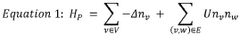
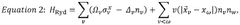


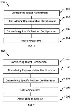
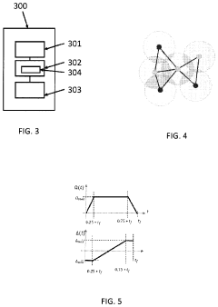
Positioning atoms using optical tweezer traps
PatentActiveUS11869678B2
Innovation
- A method using optical tweezer traps to determine a specific position configuration for atoms based on a target Hamiltonian, by evaluating similarity measures between representative Hamiltonians, which improves the likelihood of resolving the problem through adiabatic evolution and controlled positioning of atoms in a quantum computing system.
Material Science Advancements for Twistronics
The evolution of twistronics has been fundamentally driven by breakthroughs in material science. The discovery of graphene in 2004 laid the groundwork, but it was the subsequent development of precise stacking techniques that truly enabled the field to flourish. Recent advancements in van der Waals heterostructure fabrication have allowed researchers to control interlayer twist angles with unprecedented precision, down to 0.1 degrees.
Critical to these developments has been the refinement of mechanical exfoliation techniques, which now permit the isolation of atomically thin layers with minimal defects. Complementing this, chemical vapor deposition (CVD) methods have evolved to enable large-scale production of high-quality two-dimensional materials with controlled thickness and composition, essential for practical applications of twistronics.
The development of specialized transfer techniques represents another significant advancement. Dry transfer methods using polymer stamps have become increasingly sophisticated, allowing for the precise placement and alignment of 2D materials. More recently, robotic systems with computer vision capabilities have automated this process, dramatically improving reproducibility and reducing human error in the creation of twisted heterostructures.
Characterization tools have similarly undergone substantial evolution. Advanced scanning tunneling microscopy (STM) now provides atomic-resolution imaging of moiré patterns, while angle-resolved photoemission spectroscopy (ARPES) offers detailed insights into the electronic band structures that emerge from twisted configurations. These tools have been crucial in verifying theoretical predictions and guiding further material development.
Encapsulation technologies using hexagonal boron nitride (h-BN) have addressed stability challenges, protecting sensitive twisted structures from environmental degradation while preserving their unique electronic properties. This has extended the operational lifetime of twistronics devices from hours to months, making practical applications increasingly viable.
The most recent frontier involves the incorporation of atomically thin ferromagnetic and ferroelectric materials into twisted heterostructures, opening pathways to multifunctional devices that combine computational capabilities with memory functions. Additionally, research into topological materials within twisted configurations is revealing novel quantum states that could form the basis for fault-tolerant quantum computing architectures.
These material science advancements collectively represent a transformation from academic curiosity to engineering reality, progressively addressing the challenges of scalability, reproducibility, and stability that have historically limited the practical implementation of twistronics-based computational systems.
Quantum Computing Integration Possibilities
The integration of twistronics with quantum computing represents a frontier with extraordinary potential for computational advancement. Quantum systems inherently leverage quantum mechanical phenomena such as superposition and entanglement to perform calculations beyond classical capabilities. Twistronics, with its ability to manipulate electronic properties through precise atomic alignment, offers unique opportunities to enhance quantum computing architectures.
Quantum bits (qubits) currently face significant challenges related to coherence time and error rates. Twistronics-based materials, particularly magic-angle twisted bilayer graphene (MATBG), demonstrate properties that could potentially serve as novel qubit platforms. The emergent superconductivity in these materials at specific twist angles suggests possibilities for creating more stable qubits with longer coherence times, addressing one of quantum computing's fundamental limitations.
The controlled manipulation of electronic states in twisted van der Waals heterostructures could enable the development of quantum gates with unprecedented precision. Research indicates that the moiré superlattice created through twistronics might facilitate topological quantum computing approaches, which are inherently more resistant to decoherence and environmental noise than conventional quantum computing methods.
Temperature sensitivity remains a critical challenge in quantum computing, with most current systems requiring extreme cooling. Twistronics materials exhibiting room-temperature quantum phenomena could potentially reduce the extensive cooling infrastructure requirements, making quantum computing more accessible and practical for widespread implementation.
Hybrid quantum-classical computing architectures might benefit significantly from twistronics integration. The unique band structures and electronic properties of twisted materials could serve as specialized quantum processors for specific computational tasks while interfacing with classical components, creating more efficient heterogeneous computing systems.
Quantum communication networks could leverage the quantum entanglement properties potentially enhanced in twisted bilayer systems. Preliminary research suggests that twistronics-based quantum repeaters might extend the range and fidelity of quantum communication channels, essential for developing quantum internet infrastructure.
The programmability of electronic states through dynamic twist angle modulation presents intriguing possibilities for reconfigurable quantum circuits. This approach could enable adaptive quantum algorithms that optimize their architecture based on the computational problem at hand, representing a significant advancement over current fixed-architecture quantum processors.
Unlock deeper insights with Patsnap Eureka Quick Research — get a full tech report to explore trends and direct your research. Try now!
Generate Your Research Report Instantly with AI Agent
Supercharge your innovation with Patsnap Eureka AI Agent Platform!