

Twistronics and 3D Device Architectures: Current Trends.
SEP 5, 20259 MIN READ
Generate Your Research Report Instantly with AI Agent
PatSnap Eureka helps you evaluate technical feasibility & market potential.
Twistronics Evolution and Research Objectives
Twistronics emerged as a groundbreaking field in condensed matter physics following the 2018 discovery that stacking two graphene layers with a slight rotational misalignment could dramatically alter their electronic properties. This discovery, pioneered by Pablo Jarillo-Herrero's team at MIT, revealed that at specific "magic angles" of approximately 1.1 degrees, graphene bilayers exhibit unconventional superconductivity and correlated insulator states. This phenomenon opened an entirely new paradigm for engineering quantum materials through precise control of twist angles between 2D materials.
The evolution of twistronics has progressed through several distinct phases. Initially, research focused primarily on graphene-graphene interfaces, establishing fundamental principles and experimental techniques. The field subsequently expanded to include various 2D material combinations, including transition metal dichalcogenides (TMDs), hexagonal boron nitride (hBN), and other van der Waals materials. Recent developments have pushed toward more complex multilayer systems and the integration of twistronics with traditional semiconductor technologies.
Current research objectives in twistronics center on several key areas. First, researchers aim to achieve more precise control over twist angles and interlayer spacing, as even sub-degree variations can significantly impact electronic properties. Advanced fabrication techniques, including robotic assembly and self-alignment methods, are being developed to address this challenge. Second, there is growing interest in understanding and exploiting the interplay between twistronics and other quantum phenomena, such as topological states, exciton physics, and spin-valley coupling.
The integration of twistronics with 3D device architectures represents a particularly promising frontier. Traditional semiconductor scaling faces fundamental physical limits, driving interest in vertical integration and novel materials. Twistronics offers a unique approach to creating tunable electronic properties in the vertical dimension. Research objectives in this area include developing reliable methods for incorporating twisted heterostructures into conventional CMOS processes, creating hybrid devices that leverage both quantum and classical computing principles, and exploring new device concepts enabled by the unique properties of twisted interfaces.
Temperature stability remains a significant challenge, as many twistronics phenomena are currently observable only at cryogenic temperatures. A major research objective is to engineer systems that exhibit quantum properties at higher temperatures, ideally approaching room temperature operation. This involves exploring new material combinations, optimizing interlayer coupling, and developing novel device geometries that can preserve quantum coherence under practical operating conditions.
The field is also witnessing increased focus on applications beyond fundamental physics, with research objectives targeting practical implementations in quantum computing, ultra-sensitive sensors, energy-efficient electronics, and novel optoelectronic devices. These application-driven objectives are accelerating the transition from laboratory demonstrations to potentially transformative technologies.
Market Applications for Twisted 2D Materials
The market for twisted 2D materials is experiencing rapid expansion across multiple sectors due to their unique electronic, optical, and mechanical properties. In the semiconductor industry, these materials offer promising solutions for overcoming the limitations of traditional silicon-based technologies. Companies like IBM and Samsung are actively exploring twisted bilayer graphene for next-generation transistors that could potentially operate at higher speeds while consuming less power, addressing a critical need in the computing market estimated to reach $600 billion by 2025.
Telecommunications represents another significant application area, where twisted 2D materials enable the development of advanced photonic devices. The ability to precisely control the electronic band structure through twist angles creates opportunities for novel optical modulators and detectors with enhanced performance characteristics. These components are crucial for 5G and future 6G networks, where data transmission speeds and energy efficiency are paramount concerns.
Energy storage and conversion systems benefit substantially from twisted 2D materials' unique properties. Superconductivity observed in magic-angle twisted bilayer graphene opens avenues for more efficient energy transmission systems. Additionally, these materials show promise in battery technologies, potentially increasing energy density and charging rates in lithium-ion batteries, addressing key limitations in the rapidly growing electric vehicle market.
Quantum computing represents perhaps the most transformative potential application. The exotic quantum states achievable in twisted 2D heterostructures provide platforms for quantum bits (qubits) with potentially superior coherence times compared to current technologies. Companies including Google, Microsoft, and IBM have dedicated significant resources to exploring these materials for quantum computing applications, recognizing their potential to overcome existing barriers to practical quantum computers.
Sensing and medical diagnostics constitute emerging application areas with substantial growth potential. The extreme sensitivity of twisted 2D materials to environmental changes enables highly precise chemical and biological sensors. These could revolutionize medical diagnostics through more sensitive, miniaturized detection systems for biomarkers and pathogens, potentially enabling earlier disease detection and more personalized medicine approaches.
Flexible electronics represents another promising market, where the mechanical properties of twisted 2D materials allow for development of bendable, stretchable devices that maintain electronic functionality. This capability addresses growing demand for wearable technology, smart textiles, and flexible displays, markets collectively projected to exceed $30 billion annually within the next five years.
Twistronics State-of-Art and Technical Barriers
Twistronics has emerged as a revolutionary field in condensed matter physics and materials science, focusing on the manipulation of electronic properties through the precise control of twist angles between stacked 2D materials. The current state-of-art in twistronics centers around graphene-based systems, particularly magic-angle twisted bilayer graphene (MATBG), where a twist angle of approximately 1.1° leads to flat electronic bands and correlated electron phenomena including superconductivity and magnetism.
Recent advancements have expanded beyond graphene to include transition metal dichalcogenides (TMDs) such as MoS2 and WSe2, where researchers have observed moiré excitons and unique optical properties. The fabrication precision has improved significantly, with angular control now possible at the millidegree level using advanced transfer techniques and feedback mechanisms during assembly.
Despite these impressive developments, several critical technical barriers persist. Fabrication scalability remains a major challenge, as current methods rely heavily on manual, time-consuming processes that yield small-area devices with limited reproducibility. The precise control of twist angles across larger areas (>100 μm²) continues to elude researchers, hampering industrial applications.
Environmental stability presents another significant obstacle. Twistronics devices are extremely sensitive to contamination, strain, and thermal fluctuations, often requiring ultra-high vacuum or cryogenic conditions to maintain their unique properties. This sensitivity severely limits practical applications outside laboratory settings.
Interface engineering represents a frontier challenge, as the atomic-scale interactions at the interfaces between twisted layers critically determine device performance. Current understanding of these interfaces remains incomplete, particularly regarding the role of lattice reconstruction, interfacial defects, and interlayer coupling mechanisms.
Computational limitations also hinder progress, as modeling twisted systems requires enormous computational resources due to the large moiré supercells. Current simulation capabilities struggle to accurately predict properties of realistic twisted structures with defects and environmental interactions.
Integration with conventional electronics poses additional challenges. The 3D architecture necessary for practical twistronics devices requires novel interconnect solutions and packaging approaches that maintain the delicate twist configurations while providing reliable electrical connections to external circuits.
The measurement and characterization of twisted structures at relevant length scales presents ongoing difficulties, requiring advanced microscopy and spectroscopy techniques that can probe electronic and structural properties simultaneously with nanometer-scale resolution.
Current Twistronics Fabrication Approaches
01 Twistronics in 2D materials for electronic devices
Twistronics involves manipulating the electronic properties of 2D materials by controlling the twist angle between layers. This technique enables the creation of novel electronic states and properties that can be harnessed for advanced semiconductor devices. By precisely controlling the rotation angle between stacked 2D material layers, researchers can create moiré patterns that fundamentally alter the electronic band structure, leading to phenomena such as superconductivity and correlated insulator states that are valuable for next-generation electronic components.- Twistronics in 2D materials for electronic devices: Twistronics involves manipulating the electronic properties of 2D materials by controlling the twist angle between layers. This technique enables the creation of novel electronic states and properties that can be harnessed for advanced device applications. By precisely controlling the rotation angle between stacked 2D material layers, researchers can create moiré patterns that fundamentally alter electronic behavior, leading to phenomena such as superconductivity and correlated insulator states that are valuable for next-generation electronic devices.
- 3D device architectures for semiconductor integration: Three-dimensional device architectures represent a significant advancement in semiconductor technology, allowing for vertical integration of components to overcome the limitations of traditional planar designs. These architectures enable higher component density, improved performance, and reduced power consumption by stacking multiple active layers. The implementation of 3D structures in semiconductor devices facilitates more efficient interconnections between components and creates opportunities for novel functionalities that cannot be achieved with conventional 2D layouts.
- Integration of twistronics with 3D architectures: The combination of twistronics principles with 3D device architectures creates new possibilities for electronic device design and functionality. By incorporating twisted 2D material interfaces within vertically stacked structures, manufacturers can develop devices with unprecedented electronic properties and performance characteristics. This integration enables the creation of complex heterogeneous systems that leverage both the quantum effects from twisted interfaces and the spatial efficiency of 3D integration, potentially revolutionizing fields such as quantum computing, high-performance electronics, and energy-efficient devices.
- Fabrication methods for twisted heterostructures in 3D: Advanced fabrication techniques are essential for creating precisely controlled twisted heterostructures in three-dimensional device architectures. These methods include layer-by-layer assembly with controlled rotation, specialized transfer processes for maintaining alignment during stacking, and post-fabrication tuning of twist angles. Novel approaches also incorporate in-situ monitoring systems to achieve atomic-level precision in the placement and orientation of 2D materials, ensuring the desired electronic properties emerge from the twisted interfaces within complex 3D structures.
- Computational modeling and design for twistronics-based 3D devices: Computational modeling plays a crucial role in the design and optimization of twistronics-based 3D device architectures. Advanced simulation techniques enable researchers to predict the electronic properties of twisted material interfaces before physical fabrication, accelerating the development process. These computational approaches incorporate quantum mechanical calculations, molecular dynamics simulations, and machine learning algorithms to explore the vast parameter space of possible twist angles and layer combinations, identifying optimal configurations for specific device applications and performance targets.
02 3D device architecture integration with twistronics
The integration of twistronics principles into 3D device architectures represents a significant advancement in semiconductor technology. This approach combines the unique electronic properties achieved through twisted 2D material interfaces with vertical stacking and integration techniques. The resulting 3D structures offer enhanced functionality, improved performance, and higher device density compared to conventional planar architectures. These integrated designs enable novel applications in quantum computing, high-performance electronics, and energy-efficient devices.Expand Specific Solutions03 Fabrication methods for twisted heterostructures
Advanced fabrication techniques have been developed to create precisely controlled twisted heterostructures for electronic applications. These methods include layer-by-layer assembly with angular alignment control, deterministic transfer processes, and specialized growth techniques that enable the creation of twisted interfaces with atomic precision. Post-fabrication treatments and encapsulation strategies help preserve the delicate electronic states that emerge at specific twist angles, ensuring device stability and performance consistency.Expand Specific Solutions04 Computational modeling and simulation of twisted structures
Computational approaches play a crucial role in understanding and designing twistronics-based 3D device architectures. Advanced modeling techniques, including density functional theory, tight-binding models, and multiscale simulations, help predict electronic properties of twisted material systems before fabrication. These computational tools enable researchers to identify optimal twist angles for specific electronic properties, simulate device performance, and guide experimental efforts in creating functional twisted heterostructures for practical applications.Expand Specific Solutions05 Applications of twistronics in quantum information processing
Twisted 2D material systems exhibit unique quantum properties that make them promising platforms for quantum information processing. The engineered electronic states in twisted bilayers and multilayers can serve as qubits or quantum gates in quantum computing architectures. The ability to precisely control these quantum states through twist angle engineering enables the development of novel quantum devices with improved coherence times and operational fidelity. These systems also show potential for quantum sensing and quantum communication applications within 3D integrated device platforms.Expand Specific Solutions
Leading Research Groups and Industry Stakeholders
Twistronics and 3D device architectures represent an emerging frontier in semiconductor technology, currently in the early growth phase with rapidly expanding market potential. The global market is projected to reach significant scale as these technologies enable novel electronic properties and improved device performance. Leading players like Samsung Electronics, Intel, and Qualcomm are investing heavily in R&D, with Samsung demonstrating advanced twisted bilayer graphene implementations. Academic institutions including MIT and Purdue Research Foundation are contributing fundamental research, while manufacturing specialists like GlobalFoundries and TSMC are developing fabrication techniques for commercial viability. The technology is approaching the transition from laboratory demonstration to early commercial applications, with significant breakthroughs expected in the next 3-5 years.
Samsung Electronics Co., Ltd.
Technical Solution: Samsung has developed a comprehensive technical approach to twistronics and 3D device architectures that leverages their expertise in display and memory technologies. Their solution centers on a proprietary "layer-by-layer" fabrication process that enables precise control of the twist angle between 2D material sheets. Samsung's Advanced Institute of Technology has created specialized transfer equipment that can achieve angular precision of approximately 0.2 degrees across areas large enough for practical device fabrication. Their technical approach incorporates in-situ Raman spectroscopy and electrical characterization to verify the quality of twisted interfaces during the manufacturing process. Samsung has particularly focused on applications in next-generation memory architectures, where they've demonstrated prototype devices that utilize the unique electronic states in twisted van der Waals heterostructures to create multi-level storage capabilities. Their research extends to integrating these twisted structures with their existing 3D NAND and HBM (High Bandwidth Memory) technologies to create hybrid memory solutions with potentially revolutionary density and performance characteristics.
Strengths: Strong integration with existing product lines; extensive manufacturing capabilities; practical focus on commercialization pathways. Weaknesses: Less fundamental research depth compared to academic leaders; approach may be constrained by immediate commercial applications rather than exploring novel physics.
Intel Corp.
Technical Solution: Intel has developed an integrated approach to twistronics and 3D device architectures that leverages their expertise in semiconductor manufacturing. Their technical solution focuses on incorporating twisted 2D materials into their advanced 3D chip stacking technologies, particularly their Foveros 3D packaging platform. Intel's approach utilizes precision alignment techniques originally developed for their advanced lithography processes, adapted to achieve the controlled twist angles required for twistronics. Their research teams have created specialized deposition and transfer systems that can manipulate atomically thin materials with nanometer-scale precision across standard silicon wafers. Intel has also developed proprietary simulation tools that model the electronic behavior of twisted interfaces integrated within conventional semiconductor architectures. This hybrid approach aims to combine the quantum properties of twisted 2D materials with traditional CMOS technology, potentially enabling new functionalities while maintaining compatibility with existing manufacturing infrastructure.
Strengths: Extensive manufacturing infrastructure that could enable scaling; integration potential with conventional semiconductor technology; strong computational modeling capabilities. Weaknesses: Less specialized in fundamental twistronics research compared to academic institutions; approach may be limited by compatibility requirements with existing technologies.
Key Patents and Breakthroughs in Moiré Physics
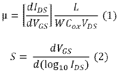
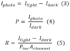
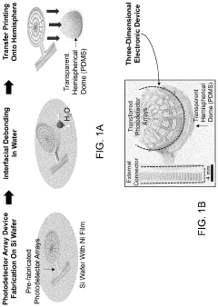
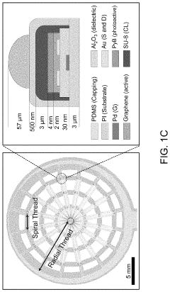
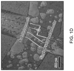
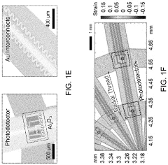
Three-dimensional electronic devices and methods of producing the same
PatentWO2022061261A1
Innovation
- A three-dimensional electronic device with a fractal structure comprising interconnected radial and spiral members, utilizing a method that includes depositing a supporting layer, patterning electrodes, forming an n-type doped graphene layer, and etching to create a fractal structure, which is then transferred onto a 3D surface, enhancing mechanical adaptability and damage tolerance.
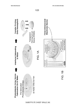
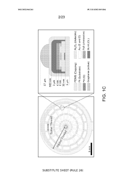
Three-dimensional electronic devices and methods of producing the same
PatentActiveUS20230288729A1
Innovation
- A three-dimensional electronic device with a fractal structure comprising interconnected radial and spiral members, utilizing a method that includes depositing a supporting layer, patterning electrodes, forming an n-type doped graphene layer, and transferring the fractal structure onto a 3D surface, enhancing mechanical adaptability and optoelectronic performance.
Materials Science Challenges in 3D Device Implementation
The implementation of twistronics in 3D device architectures presents significant materials science challenges that must be addressed for successful commercialization. The precise control of atomic-level interfaces between twisted layers requires unprecedented manufacturing precision, with angular alignment tolerances often below 0.1 degrees. This level of precision exceeds the capabilities of current industrial-scale fabrication techniques, necessitating the development of new methodologies for consistent production.
Material compatibility issues arise when integrating twisted 2D materials into conventional 3D device stacks. The thermal expansion coefficient mismatch between twisted 2D layers and traditional semiconductor materials can lead to strain-induced delamination or performance degradation during thermal cycling. Additionally, the chemical stability of these interfaces under standard semiconductor processing conditions remains questionable, with evidence suggesting potential degradation during exposure to common etching and deposition processes.
Defect management represents another critical challenge. Point defects, dislocations, and grain boundaries in the constituent 2D materials can disrupt the moiré superlattice formation that underlies twistronics phenomena. These defects propagate differently in 3D architectures compared to planar configurations, requiring new theoretical models and experimental techniques for characterization and mitigation.
The scalable synthesis of high-quality 2D materials suitable for twistronics applications remains elusive. While laboratory demonstrations utilize mechanically exfoliated flakes with near-perfect crystallinity, industrial implementation requires chemical vapor deposition (CVD) or other scalable growth techniques that currently produce materials with higher defect densities and smaller domain sizes than ideal for twistronics applications.
Contact engineering presents unique challenges in twisted heterostructures. The complex band structure modifications induced by twisting create unconventional electronic states that do not form traditional ohmic or Schottky contacts with standard electrode materials. Novel contact materials and geometries must be developed to efficiently inject and extract carriers from these exotic electronic states without disrupting the delicate twisted interface physics.
Finally, encapsulation and packaging solutions must be developed that protect the sensitive twisted interfaces from environmental degradation while maintaining their unique electronic properties. Conventional passivation techniques often introduce interfacial strain or chemical modifications that can destroy the desired twistronics effects, necessitating new approaches specifically designed for these novel material systems.
Quantum Computing Implications of Twistronics
Twistronics represents a revolutionary approach in materials science that could significantly impact quantum computing development. The manipulation of twist angles between stacked 2D materials creates unique electronic properties that may serve as platforms for quantum bits (qubits) with enhanced coherence times and reduced error rates. This potential stems from the emergence of strongly correlated electron states in twisted bilayer systems, which could provide more stable quantum states than conventional approaches.
The discovery of superconductivity in magic-angle twisted bilayer graphene offers particularly promising applications for quantum computing. These systems exhibit robust quantum states that could be less susceptible to environmental decoherence—one of the primary challenges in quantum computing. Furthermore, the ability to precisely control electronic properties through twist angles provides a tunable platform for quantum gate operations, potentially enabling more efficient quantum algorithms.
Recent experimental demonstrations have shown that twistronics-based devices can maintain quantum coherence at higher temperatures than traditional superconducting qubits. This temperature advantage could significantly reduce the cooling requirements for quantum processors, making quantum computing systems more practical and energy-efficient. Additionally, the inherent topological properties of certain twisted material systems might support topologically protected quantum states, offering a pathway toward fault-tolerant quantum computation.
The integration of twistronics with 3D device architectures presents opportunities for scalable quantum computing architectures. Vertical stacking of multiple twisted layers could enable 3D quantum circuits with higher qubit densities and more complex interconnections than planar designs. This approach aligns with the quantum computing industry's push toward more compact and powerful quantum processors capable of tackling increasingly complex computational problems.
Several research groups have begun exploring hybrid systems that combine twistronics-based qubits with conventional quantum computing technologies. These hybrid approaches could leverage the strengths of different quantum platforms while mitigating their individual weaknesses. For instance, twisted bilayer graphene qubits might serve as quantum memory elements with long coherence times, while superconducting circuits could handle rapid gate operations.
The path toward practical twistronics-based quantum computing faces significant challenges, including material fabrication precision, interface quality control, and scalable manufacturing techniques. However, if these challenges can be overcome, twistronics could potentially enable quantum computers that operate at higher temperatures, with greater qubit densities, and improved error correction capabilities—representing a transformative advance in quantum computing technology.
Unlock deeper insights with PatSnap Eureka Quick Research — get a full tech report to explore trends and direct your research. Try now!
Generate Your Research Report Instantly with AI Agent
Supercharge your innovation with PatSnap Eureka AI Agent Platform!