Twistronics and the Emergence of Moiré Patterns.
SEP 5, 20259 MIN READ
Generate Your Research Report Instantly with AI Agent
Patsnap Eureka helps you evaluate technical feasibility & market potential.
Twistronics Background and Research Objectives
Twistronics emerged as a groundbreaking field in condensed matter physics following the pivotal discovery in 2018 by researchers at MIT, who demonstrated that graphene sheets, when stacked at specific "magic angles," can exhibit remarkable properties including superconductivity. This discovery marked a paradigm shift in understanding how the relative orientation between two-dimensional material layers can fundamentally alter their electronic behavior through the formation of moiré patterns.
The historical development of twistronics can be traced back to earlier theoretical work on twisted bilayer systems, but the experimental confirmation of its profound implications has accelerated research dramatically in the past five years. The field represents the intersection of quantum mechanics, materials science, and nanotechnology, focusing on how the twist angle between stacked 2D materials creates periodic potentials that modify electron behavior.
Moiré patterns, the visual interference patterns that emerge when two similar lattices are overlaid with a relative rotation, serve as the fundamental physical phenomenon underlying twistronics. These patterns effectively create a "superlattice" with a periodicity much larger than the original atomic lattice, leading to the formation of flat electronic bands and strongly correlated electron states at specific twist angles.
The primary research objectives in the field of twistronics currently focus on several key areas. First, researchers aim to develop precise control mechanisms for creating and manipulating twist angles in 2D material heterostructures, as even sub-degree variations can dramatically alter electronic properties. Second, there is significant interest in expanding the materials palette beyond graphene to include other 2D materials such as transition metal dichalcogenides, hexagonal boron nitride, and various heterostructures.
Another critical research direction involves understanding the fundamental physics of strongly correlated electron systems in twisted structures, particularly the mechanisms behind unconventional superconductivity, magnetism, and topological phases that emerge at specific twist angles. This understanding could potentially lead to room-temperature superconductors, a long-sought goal in materials science.
The technological implications of twistronics extend beyond basic science to potential applications in quantum computing, ultra-efficient electronics, and novel sensing technologies. As such, research objectives also include developing scalable fabrication methods that can precisely control twist angles in large-area samples, a necessary step for industrial applications.
The field is currently experiencing exponential growth in research activity, with major investments from both academic institutions and technology companies seeking to harness these novel quantum phenomena for next-generation technologies. This research trajectory suggests that twistronics will continue to be a frontier area in condensed matter physics and materials science for the foreseeable future.
Market Applications of Moiré Pattern Technologies
Moiré pattern technologies are rapidly transitioning from laboratory curiosities to commercial applications across multiple industries. The unique physical properties that emerge when two-dimensional materials are stacked with slight rotational misalignment create unprecedented opportunities for technological innovation. Current market applications are expanding in several key sectors, with electronics and optoelectronics leading the commercialization efforts.
In the semiconductor industry, moiré superlattices are being explored for next-generation transistors and memory devices. Companies like IBM and Samsung have invested significantly in twistronics research, recognizing its potential to overcome silicon's physical limitations. These technologies promise higher electron mobility and novel quantum states that could revolutionize computing architecture. Market analysts project that moiré-based semiconductor components could capture a specialized segment of the high-performance computing market within the next five years.
The optical sensing and imaging sector represents another promising application area. Moiré patterns' extreme sensitivity to strain and deformation makes them ideal for high-precision sensors. Several startups have developed prototype strain gauges and pressure sensors based on twisted bilayer graphene that demonstrate sensitivity orders of magnitude greater than conventional technologies. These sensors are finding applications in structural health monitoring, aerospace, and biomedical devices where nanoscale precision is critical.
Quantum computing represents perhaps the most transformative potential market for moiré technologies. The unique quantum states that emerge in twisted bilayer systems provide a novel platform for quantum bit (qubit) implementation. Research institutions and quantum computing companies are investigating how moiré-induced superconductivity might create more stable qubits with longer coherence times. While commercial quantum computers based on this technology remain years away, substantial research funding is flowing into this area.
Energy storage and conversion applications are also emerging as promising markets. Researchers have demonstrated that controlling the twist angle between layers of certain 2D materials can dramatically alter their catalytic properties, potentially improving the efficiency of hydrogen production and carbon dioxide reduction reactions. Several clean energy startups are developing prototype electrochemical cells that leverage these properties for more efficient energy conversion.
The telecommunications sector is exploring moiré superlattices for next-generation photonic devices. The ability to precisely tune the electronic and optical properties of these materials by adjusting the twist angle offers new possibilities for optical modulators, detectors, and switches operating at unprecedented speeds and energy efficiencies. Major telecommunications equipment manufacturers have begun incorporating early versions of these components into their product development roadmaps.
While mass-market applications remain limited by manufacturing challenges and cost factors, the specialized high-value markets described above are driving initial commercialization efforts. Industry analysts expect the total addressable market for moiré pattern technologies to grow substantially as manufacturing processes mature and costs decrease.
Current Challenges in Twistronics Research
Despite significant advancements in twistronics research since its emergence in 2018, the field faces several substantial challenges that impede further progress. One primary obstacle is the precise control of twist angles between stacked 2D materials. Current fabrication techniques struggle to achieve consistent and reproducible twist angles at the sub-degree level, which is critical as even minor deviations can dramatically alter the resulting moiré patterns and electronic properties. This fabrication precision challenge becomes increasingly complex when working with materials beyond graphene, such as transition metal dichalcogenides.
Material quality and homogeneity represent another significant hurdle. The presence of defects, wrinkles, and strain in 2D materials can disrupt the formation of moiré patterns and introduce unwanted electronic states. These imperfections become particularly problematic at the industrial scale, where maintaining consistent quality across large-area samples remains elusive. The field currently lacks standardized quality control protocols specific to twisted heterostructures.
Characterization techniques also present limitations. While scanning tunneling microscopy provides atomic-level insights, it remains time-consuming and limited to small sample areas. Optical techniques offer faster characterization but with reduced resolution. The development of non-destructive, high-throughput characterization methods that can accurately map twist angles and moiré patterns across entire devices remains an open challenge.
The theoretical understanding of twistronics systems beyond magic-angle twisted bilayer graphene is still developing. Current computational models struggle with the immense complexity of moiré superlattices, which can contain thousands of atoms per unit cell. This computational challenge limits accurate predictions of properties in complex heterostructures involving multiple twisted layers or diverse material combinations.
Temperature stability presents another significant barrier. Many exotic quantum phenomena in twisted systems, such as superconductivity and correlated insulator states, manifest only at extremely low temperatures (typically below 10K). Developing twistronics-based devices that operate at practical temperatures remains a formidable challenge that limits commercial applications.
Finally, the field faces integration challenges with existing semiconductor technology. Incorporating twisted 2D heterostructures into conventional electronic platforms requires developing compatible fabrication processes, addressing issues of contact resistance, and ensuring long-term device stability. The gap between laboratory demonstrations and commercially viable technologies remains substantial, necessitating interdisciplinary approaches combining materials science, device engineering, and quantum physics.
Current Approaches to Moiré Pattern Engineering
01 Twistronics in 2D materials
Twistronics involves the manipulation of electronic properties in 2D materials by creating moiré patterns through the rotation of layers at specific angles. This technique allows for the engineering of novel quantum states and electronic behaviors in layered materials such as graphene. The moiré patterns that emerge from the twisted layers create superlattice structures that can dramatically alter the material's properties, enabling applications in quantum computing and advanced electronics.- Twistronics in 2D materials: Twistronics involves the manipulation of electronic properties in 2D materials by creating moiré patterns through the rotation of atomic layers at specific angles. This technique allows for the engineering of novel quantum states and electronic behaviors in layered materials such as graphene. The moiré superlattices formed by twisting layers relative to each other can dramatically alter the band structure and create unique electronic phenomena including superconductivity and correlated insulator states.
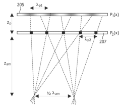
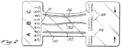
- Optical detection and imaging of moiré patterns: Various optical methods and systems have been developed to detect, analyze, and visualize moiré patterns. These techniques include specialized microscopy, interferometry, and imaging systems that can capture the subtle interference patterns created when periodic structures overlap. Advanced optical detection systems enable precise measurement of moiré patterns for applications in material science, strain analysis, and quality control in manufacturing processes.
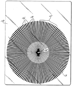
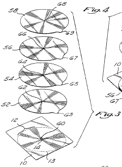
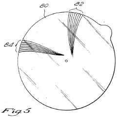
- Moiré pattern analysis for authentication and security: Moiré patterns are utilized in security and authentication applications due to their unique visual properties that are difficult to replicate. By incorporating specific moiré-generating structures into documents, products, or digital media, distinctive visual effects can be created that serve as anti-counterfeiting features. These patterns can be designed to reveal hidden information or change appearance when viewed from different angles or when overlaid with a specific key pattern.
- Computational methods for moiré pattern simulation: Advanced computational techniques have been developed to simulate, predict, and analyze moiré patterns in various materials and structures. These methods include mathematical modeling, numerical algorithms, and software tools that can calculate the formation of moiré superlattices based on layer orientation, lattice parameters, and other physical properties. Computational approaches enable researchers to design twistronics devices with specific electronic properties by predicting the behavior of moiré patterns before physical fabrication.
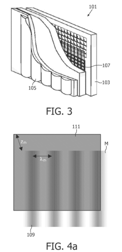
- Manufacturing processes for controlled moiré structures: Specialized fabrication techniques have been developed to create precisely controlled moiré patterns in layered materials. These manufacturing processes include methods for accurate layer alignment, controlled rotation of atomic layers, and techniques to maintain the integrity of interfaces between layers. Advanced deposition, transfer, and patterning methods enable the creation of twistronics devices with specific moiré superlattices for applications in quantum computing, electronics, and optoelectronics.
02 Optical detection and imaging of moiré patterns
Various optical methods have been developed to detect, analyze, and image moiré patterns in materials. These techniques include specialized microscopy, interferometry, and optical sensing systems that can visualize the interference patterns created by overlapping lattice structures. These imaging methods are crucial for characterizing twistronics devices and understanding the relationship between structural configuration and electronic properties in twisted layered materials.Expand Specific Solutions03 Fabrication techniques for controlled moiré structures
Advanced fabrication methods have been developed to create precisely controlled moiré patterns in layered materials. These techniques include layer transfer processes, controlled rotation mechanisms, and specialized deposition methods that enable the creation of specific twist angles between layers. The ability to fabricate structures with well-defined moiré patterns is essential for developing practical twistronics devices with reproducible properties.Expand Specific Solutions04 Moiré pattern analysis and authentication applications
Moiré patterns have applications in security and authentication systems. The unique interference patterns created when overlaying structured patterns can be used for document security, anti-counterfeiting measures, and verification systems. These applications leverage the sensitivity of moiré patterns to small changes in alignment, making them difficult to reproduce without precise knowledge of the original patterns.Expand Specific Solutions05 Computational modeling of twistronics phenomena
Computational methods have been developed to model and predict the electronic and optical properties of twisted layered materials. These approaches include quantum mechanical simulations, density functional theory calculations, and continuum models that can predict the behavior of moiré superlattices. Computational modeling is essential for understanding the complex physics of twistronics and for designing materials with specific electronic properties.Expand Specific Solutions
Leading Research Groups and Industry Players
Twistronics and moiré patterns represent an emerging field in quantum materials research, currently in its early growth phase. The market is expanding rapidly with an estimated size of $50-100 million, expected to grow significantly as applications in quantum computing and advanced electronics materialize. The technology is transitioning from fundamental research to early commercialization, with academic institutions like École Polytechnique Fédérale de Lausanne and Hefei University of Technology leading fundamental discoveries. Companies including TOPPAN, Renesas Electronics, and LG Electronics are beginning to explore commercial applications, while specialized firms like Cambridge Touch Technologies are developing practical implementations for consumer electronics. The competitive landscape features collaboration between research institutions and industry players, with increasing patent activity signaling the technology's growing commercial potential.
École Polytechnique Fédérale de Lausanne
Technical Solution: École Polytechnique Fédérale de Lausanne (EPFL) has pioneered research in twistronics, focusing on the manipulation of electronic properties in 2D materials through precise angular alignment. Their approach involves creating moiré superlattices by stacking two-dimensional materials with a slight rotational misalignment, which generates new quantum states and electronic behaviors. EPFL researchers have developed advanced fabrication techniques that allow for atomic-level precision in creating twisted heterostructures, particularly with graphene and transition metal dichalcogenides. Their work has demonstrated that at specific "magic angles" of rotation (approximately 1.1°), graphene layers can exhibit unconventional superconductivity and correlated insulator states. EPFL has also created specialized equipment for in-situ measurement of electronic properties while controlling twist angles, enabling real-time observation of emergent phenomena in moiré patterns.
Strengths: EPFL possesses world-class nanofabrication facilities and expertise in quantum materials, allowing for precise control of twist angles and layer stacking. Their interdisciplinary approach combines theoretical physics, materials science, and engineering. Weaknesses: The fabrication processes remain challenging to scale beyond laboratory samples, and maintaining consistent twist angles across larger areas presents significant manufacturing hurdles.
Changchun Institute of Optics Fine Mechanics & Physics
Technical Solution: Changchun Institute of Optics Fine Mechanics & Physics has developed innovative optical approaches to twistronics research, leveraging their expertise in precision optics and photonics. Their technical solution involves using advanced optical characterization techniques to study moiré patterns in twisted 2D materials. They've created specialized optical systems that can detect and analyze the subtle interference patterns created by twisted layers with nanometer precision. Their approach combines scanning near-field optical microscopy (SNOM) with custom spectroscopic techniques to map the electronic and optical properties of moiré superlattices in real space. The institute has also pioneered non-destructive optical methods to determine twist angles in encapsulated heterostructures, which is crucial for correlating structure with emergent quantum properties. Their research extends to photonic applications of moiré patterns, exploring how the periodic potential modulations can be used to control light-matter interactions at the nanoscale.
Strengths: The institute excels in optical characterization techniques that provide unique insights into moiré physics without damaging delicate samples. Their expertise in precision optics enables high-resolution imaging of quantum phenomena. Weaknesses: Their approach is primarily focused on characterization rather than fabrication, potentially limiting their ability to create novel twisted structures with precisely controlled properties.
Key Breakthroughs in Twistronics Theory
Display Device with Homogenising Attentuating Filter
PatentInactiveUS20080316604A1
Innovation
- An optical attenuator arrangement with a light attenuation characteristic that varies across the display area is positioned in front of the display device, complementing the inherent non-uniformity to achieve uniform output intensity, using thin light attenuation panels or sheets with specific attenuation patterns to cancel out moiré and other non-uniformities.
Device for creating and displaying moire patterns
PatentInactiveUS4976620A
Innovation
- A device comprising a base plate with an array of lines and multiple transparent upper plates with similar line arrays that can be rotated to produce shimmering moire patterns, allowing for the creation of unique and complex patterns through various line combinations, colors, and user-designed arrays using a line-drawing template.
Materials Fabrication Techniques
The fabrication of materials for twistronics research requires precise control at the atomic level, with several key techniques emerging as essential for creating high-quality moiré superlattices. Mechanical exfoliation, pioneered during the initial graphene discovery, remains fundamental for producing pristine two-dimensional (2D) materials. This method involves using adhesive tape to peel atomically thin layers from bulk crystals, providing samples with minimal defects and contamination crucial for observing quantum phenomena in twisted structures.
Chemical vapor deposition (CVD) has evolved as a scalable alternative, enabling the growth of large-area 2D materials with controlled thickness. Recent advancements in CVD techniques have achieved precise control over growth parameters, allowing researchers to synthesize materials with predetermined twist angles directly during growth. This represents a significant step toward industrial-scale production of twisted heterostructures.
The deterministic transfer method stands as perhaps the most critical technique in twistronics research. This approach utilizes micromanipulators and specialized polymer stamps to pick up and stack 2D materials with angular precision better than 0.1 degrees. The development of "tear-and-stack" methods has further refined this process, where a single flake is torn and one piece is rotated before restacking, ensuring crystallographic alignment between layers.
Molecular beam epitaxy (MBE) offers another sophisticated approach for creating twisted interfaces with exceptional purity. By depositing materials in ultra-high vacuum conditions, researchers can grow heterostructures with atomically sharp interfaces and minimal contamination, critical for preserving the delicate electronic states in moiré patterns.
Post-fabrication techniques have also emerged as essential components of the twistronics toolkit. These include encapsulation with hexagonal boron nitride (h-BN) to protect samples from environmental degradation, and the use of specialized annealing protocols to remove trapped contaminants and achieve atomically clean interfaces between layers.
Recent innovations include the development of "twist-on-demand" techniques that allow for in-situ adjustment of the twist angle through strain engineering or the application of external fields. These approaches enable dynamic tuning of moiré patterns, opening new possibilities for reconfigurable quantum devices based on twistronics principles.
Quantum Properties and Device Applications
The quantum properties of twisted bilayer systems represent one of the most fascinating aspects of twistronics research. When two-dimensional materials are stacked with a slight rotational misalignment, the resulting moiré superlattice creates a periodic potential that fundamentally alters the electronic band structure. In magic-angle twisted bilayer graphene (approximately 1.1°), the electronic bands near the Fermi level become remarkably flat, dramatically enhancing electron-electron interactions and giving rise to a variety of quantum phenomena including unconventional superconductivity and correlated insulator states.
These quantum states emerge from the delicate interplay between the moiré potential, electron correlations, and band topology. Recent experimental observations have confirmed the presence of topologically protected edge states and quantum anomalous Hall effects in certain twisted material systems, particularly when combined with magnetic proximity effects or when intrinsic magnetism is present.
The quantum properties of twisted van der Waals heterostructures extend beyond electronic correlations to include novel optical phenomena. Excitons (bound electron-hole pairs) in these systems can become localized within the moiré potential wells, creating "moiré excitons" with distinct optical signatures. These quantum-confined excitons exhibit narrow linewidths and valley-selective optical responses that could be harnessed for quantum information applications.
Device applications leveraging these quantum properties are rapidly emerging across multiple technological domains. Quantum computing represents a particularly promising frontier, with proposals for qubits based on valley states or localized electronic states in moiré superlattices. The long coherence times potentially achievable in these systems make them attractive candidates for quantum information processing.
In sensing applications, the extreme sensitivity of the quantum states in twisted bilayer systems to external perturbations enables the development of ultrasensitive detectors for magnetic fields, strain, and chemical species. The distinct optical transitions associated with moiré excitons also provide opportunities for novel optoelectronic devices, including tunable light emitters and photodetectors operating across a wide spectral range.
Energy applications are equally compelling, with the flat bands in magic-angle twisted bilayer graphene potentially enabling more efficient thermoelectric conversion. The unconventional superconductivity observed in these systems, while currently limited to low temperatures, offers tantalizing possibilities for future energy transmission technologies if higher transition temperatures can be achieved through materials engineering.
Unlock deeper insights with Patsnap Eureka Quick Research — get a full tech report to explore trends and direct your research. Try now!
Generate Your Research Report Instantly with AI Agent
Supercharge your innovation with Patsnap Eureka AI Agent Platform!