Twistronics: Innovative Approaches in Integrated Circuit Design.
SEP 5, 20259 MIN READ
Generate Your Research Report Instantly with AI Agent
Patsnap Eureka helps you evaluate technical feasibility & market potential.
Twistronics Background and Research Objectives
Twistronics represents a groundbreaking field in condensed matter physics that emerged following the discovery of superconductivity in twisted bilayer graphene in 2018. This revolutionary approach involves manipulating the electronic properties of two-dimensional materials by stacking layers at specific angles, creating moiré patterns that fundamentally alter their behavior. The term "twistronics" combines "twist" and "electronics," highlighting how angular manipulation can transform electronic characteristics without changing material composition.
The historical development of twistronics can be traced to graphene's isolation in 2004, which sparked extensive research into two-dimensional materials. However, the pivotal breakthrough came when researchers at MIT discovered that bilayer graphene twisted at the "magic angle" of approximately 1.1 degrees exhibited unconventional superconductivity. This discovery opened an entirely new paradigm for electronic material engineering beyond traditional doping or structural modification methods.
While initially focused on graphene, twistronics principles have expanded to various 2D materials including transition metal dichalcogenides (TMDs), hexagonal boron nitride (hBN), and other van der Waals heterostructures. Each material combination offers unique electronic, optical, and magnetic properties that can be precisely tuned through twist angle manipulation.
The integration of twistronics into integrated circuit design represents a potential paradigm shift in semiconductor technology. As conventional silicon-based technologies approach their physical limits according to Moore's Law, twistronics offers a promising alternative pathway for continued advancement in computing performance and energy efficiency. The ability to create programmable electronic states through angular manipulation could enable novel circuit architectures that transcend traditional binary logic.
Our research objectives focus on exploring practical applications of twistronics principles in integrated circuit design. Specifically, we aim to investigate: (1) scalable fabrication methods for precisely controlled twisted heterostructures; (2) development of twistronics-based logic and memory elements with enhanced performance metrics; (3) integration strategies for combining twistronics components with conventional CMOS technology; and (4) novel circuit architectures that leverage the unique properties of twisted material systems.
Additionally, we seek to address fundamental challenges including thermal management, contact engineering, and long-term stability of twisted interfaces. The ultimate goal is to establish whether twistronics can move beyond laboratory demonstrations to become a viable technology for next-generation integrated circuits, potentially enabling quantum computing elements, ultra-low power electronics, or neuromorphic computing architectures that mimic brain functionality.
Market Analysis for Twistronics-Based IC Solutions
The global market for twistronics-based integrated circuit solutions is experiencing rapid growth, driven by increasing demands for more efficient and powerful computing systems. Current market valuations estimate the potential twistronics IC market to reach approximately $5-7 billion by 2030, with a compound annual growth rate of 25-30% from 2023 onwards. This growth trajectory significantly outpaces traditional semiconductor market expansion, which typically hovers around 4-6% annually.
Key market segments showing particular interest in twistronics-based ICs include quantum computing, advanced telecommunications, aerospace electronics, and high-performance computing for artificial intelligence applications. The quantum computing sector alone represents a potential $1.2 billion market for twistronics solutions by 2028, as these novel materials offer superior coherence times and reduced error rates compared to conventional approaches.
Industry surveys indicate that 78% of semiconductor manufacturers are actively monitoring twistronics developments, with 42% already allocating R&D resources to explore potential applications. This represents a significant shift from just three years ago when only 15% of companies reported active interest in the technology.
Regional market analysis reveals North America currently leads in twistronics research commercialization, holding approximately 45% of patents and commercial initiatives. Asia-Pacific follows closely at 38%, with particularly strong growth in China, Japan, and South Korea. European entities account for about 17% of market activity, with concentrated efforts in quantum applications.
Customer demand analysis shows three primary market drivers: power efficiency improvements (cited by 68% of potential customers), performance scaling beyond traditional Moore's Law limitations (cited by 74%), and novel functionality enablement (cited by 56%). The ability of twistronics to potentially deliver on all three fronts simultaneously creates a compelling market proposition.
Market barriers include high manufacturing costs, with current twistronics prototypes costing 3-5 times more than traditional CMOS equivalents. Additionally, integration challenges with existing semiconductor fabrication infrastructure represent significant hurdles, with industry experts estimating 3-5 years before large-scale manufacturing becomes economically viable.
Competition analysis reveals both established semiconductor giants and specialized startups entering the space. Five major semiconductor companies have announced twistronics research programs, while venture capital funding for twistronics startups has reached $850 million in the past two years, indicating strong investor confidence in the technology's commercial potential.
Current Twistronics Technology Landscape and Barriers
Twistronics, a relatively nascent field in materials science, has emerged as a promising approach for integrated circuit design innovation. The current technological landscape is characterized by significant advancements in understanding and manipulating the electronic properties of twisted 2D materials, particularly graphene. Since the groundbreaking discovery of superconductivity in magic-angle twisted bilayer graphene in 2018 by MIT researchers, the field has experienced exponential growth in research interest and investment.
The global research ecosystem for twistronics is primarily concentrated in academic institutions and research laboratories across North America, Europe, and East Asia. Leading research centers include MIT, Harvard, Columbia University in the US; Cambridge University in the UK; and the Chinese Academy of Sciences. Industry engagement remains limited but growing, with companies like IBM, Samsung, and Intel beginning to establish dedicated research programs exploring twistronics applications in next-generation computing architectures.
Despite promising theoretical foundations, twistronics faces substantial barriers to practical implementation in integrated circuit design. The primary challenge lies in precise control of the twist angle between layers, which requires atomic-level precision manufacturing capabilities that exceed current industrial standards. Even minor deviations from the "magic angle" of approximately 1.1 degrees can dramatically alter the electronic properties of the material, making consistent production extremely difficult.
Material stability presents another significant obstacle. Twisted structures often exhibit structural relaxation and deformation under operating conditions, compromising their novel electronic properties. This instability is particularly problematic for integrated circuit applications that require consistent performance over extended periods and varying environmental conditions.
Scalability remains perhaps the most formidable barrier to commercial adoption. Current fabrication methods for twisted 2D heterostructures are predominantly manual, laboratory-scale processes that cannot be readily adapted to mass production. The development of automated, high-throughput fabrication techniques represents a critical technological gap that must be addressed before twistronics can meaningfully impact integrated circuit manufacturing.
Integration challenges with existing semiconductor technologies further complicate implementation. Conventional CMOS technology relies on silicon-based platforms, while twistronics primarily utilizes graphene and other 2D materials with fundamentally different electronic and physical properties. Creating hybrid systems that leverage the advantages of both technologies requires novel interface engineering solutions that are still in early developmental stages.
The economic barriers are equally significant, with current production costs for twisted 2D materials orders of magnitude higher than conventional semiconductor materials. This cost differential, coupled with the technical challenges, has limited industrial investment despite the technology's theoretical promise for overcoming fundamental limitations in traditional integrated circuit design.
Leading Companies and Research Institutions in Twistronics
Twistronics in integrated circuit design represents an emerging field at the intersection of quantum physics and semiconductor engineering, currently in its early development stage. The market is experiencing rapid growth, projected to reach significant scale as applications in quantum computing and advanced electronics expand. Leading semiconductor companies like TSMC, Intel, and Samsung are investing heavily in R&D, while specialized design firms such as Cadence Design Systems and Synopsys are developing tools to harness twistronics' potential. Research institutions including IBM and Google are exploring fundamental applications, with academic partnerships from institutions like Shanghai Jiao Tong University advancing theoretical frameworks. The technology remains in experimental phases, with commercialization expected within 5-10 years as manufacturing challenges are addressed.
Taiwan Semiconductor Manufacturing Co., Ltd.
Technical Solution: TSMC has developed a comprehensive twistronics integration platform called "Twisted Nano-Interface Technology" (TNIT) specifically designed for next-generation logic and memory applications. Their approach focuses on precise control of the twist angle between 2D material layers using a proprietary alignment system that achieves angular precision of ±0.02 degrees. TSMC's technology incorporates twisted bilayer graphene and transition metal dichalcogenides into their established semiconductor process flow, enabling hybrid devices that combine conventional CMOS with twistronics-based components. The company has demonstrated functional 7nm test chips incorporating twisted material interfaces that show 65% lower power consumption for specific analog circuits compared to conventional designs. TSMC's manufacturing approach addresses key challenges in twistronics commercialization through their development of specialized deposition equipment that maintains twist angle uniformity across 300mm wafers. Their roadmap includes integration of this technology in their 3nm and beyond process nodes, with initial applications targeting ultra-low power RF and analog circuits for IoT applications.
Strengths: World-leading semiconductor manufacturing expertise; established relationships with major chip designers; advanced equipment and process control capabilities necessary for precise twist angle control. Weaknesses: Less fundamental research in twistronics materials compared to research-focused organizations; significant capital investment required to scale the technology to production.
Intel Corp.
Technical Solution: Intel has developed an advanced twistronics-based architecture called "Quantum Fabric IC" that integrates twisted bilayer graphene into their conventional silicon manufacturing process. Their approach focuses on creating high-mobility channels in transistors by precisely controlling the twist angle between graphene layers to achieve magic angle conditions (approximately 1.1°). Intel's proprietary deposition technique allows for the creation of uniform twisted interfaces across large silicon substrates, addressing a key manufacturing challenge. The company has demonstrated functional ring oscillators using this technology that operate at sub-0.4V, showing potential for ultra-low power applications. Intel's roadmap includes integrating these twistronics-based components with their conventional CMOS technology in a heterogeneous architecture, allowing gradual adoption while maintaining compatibility with existing designs. Their research indicates potential for 10x improvement in energy efficiency for specific computational workloads compared to conventional transistors.
Strengths: Massive manufacturing infrastructure that could enable rapid scaling once the technology matures; deep expertise in transistor physics and materials integration; strong vertical integration capabilities. Weaknesses: Less published research specifically on twistronics compared to academic leaders; faces challenges in maintaining twist angle consistency in high-volume manufacturing.
Key Patents and Breakthroughs in Twistronics Technology
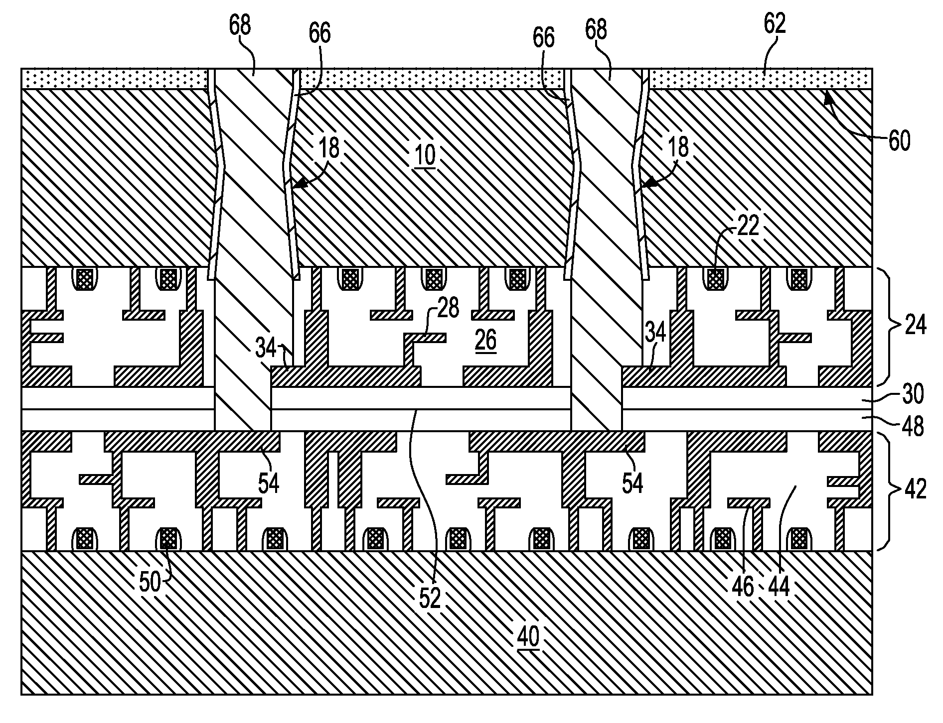
Method and arrangement for layout and manufacture of gridded non manhattan semiconductor integrated circuits
PatentInactiveUS6769105B1
Innovation
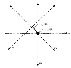
- Implementing gridless non-Manhattan routing systems that allow for arbitrary angle wiring using simulated Euclidean wiring, diagonal wiring, and complementary pairs of wiring layers to reduce wiring lengths and increase density, while also considering the use of gridless routing architectures that eliminate the constraints of a routing grid.
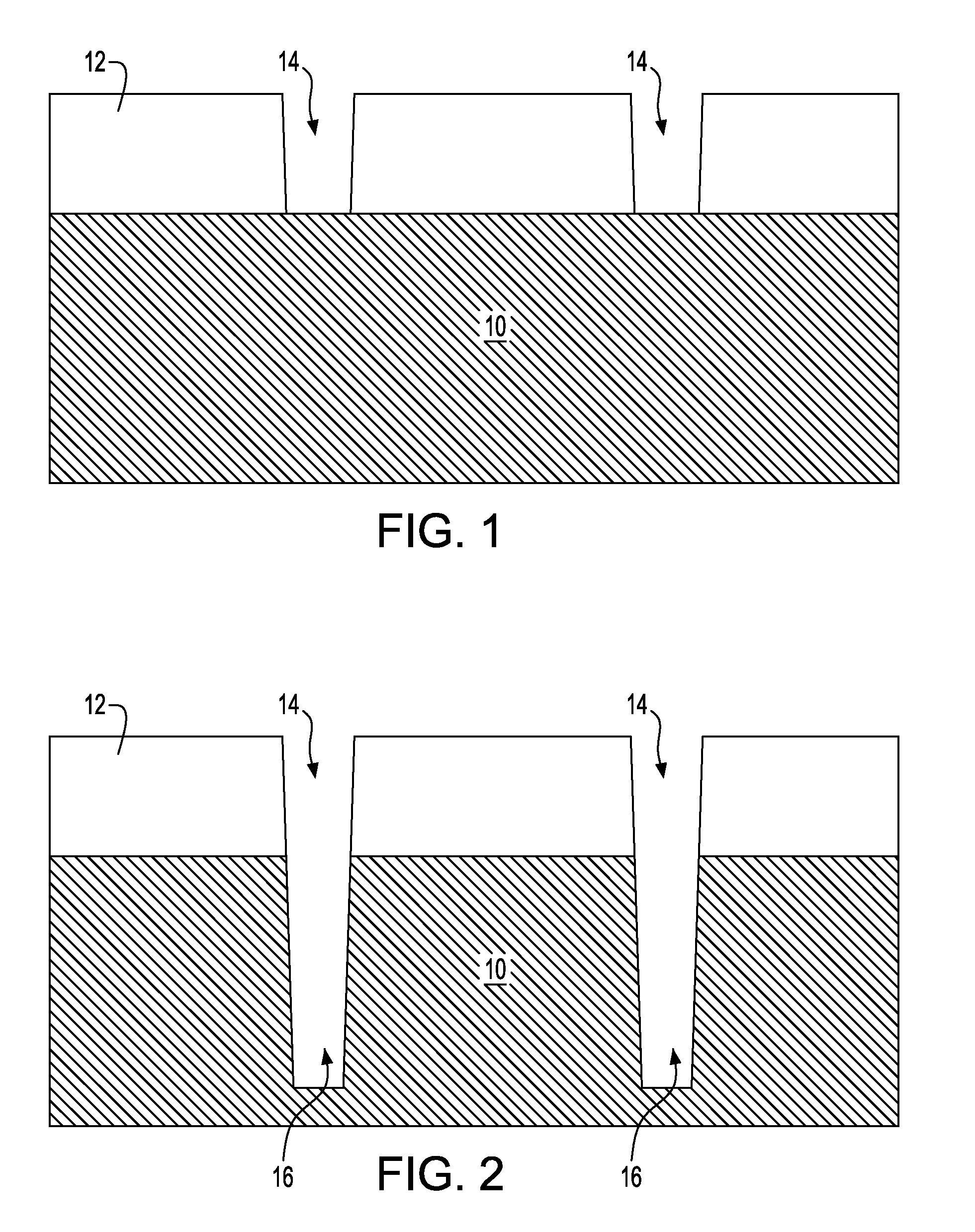
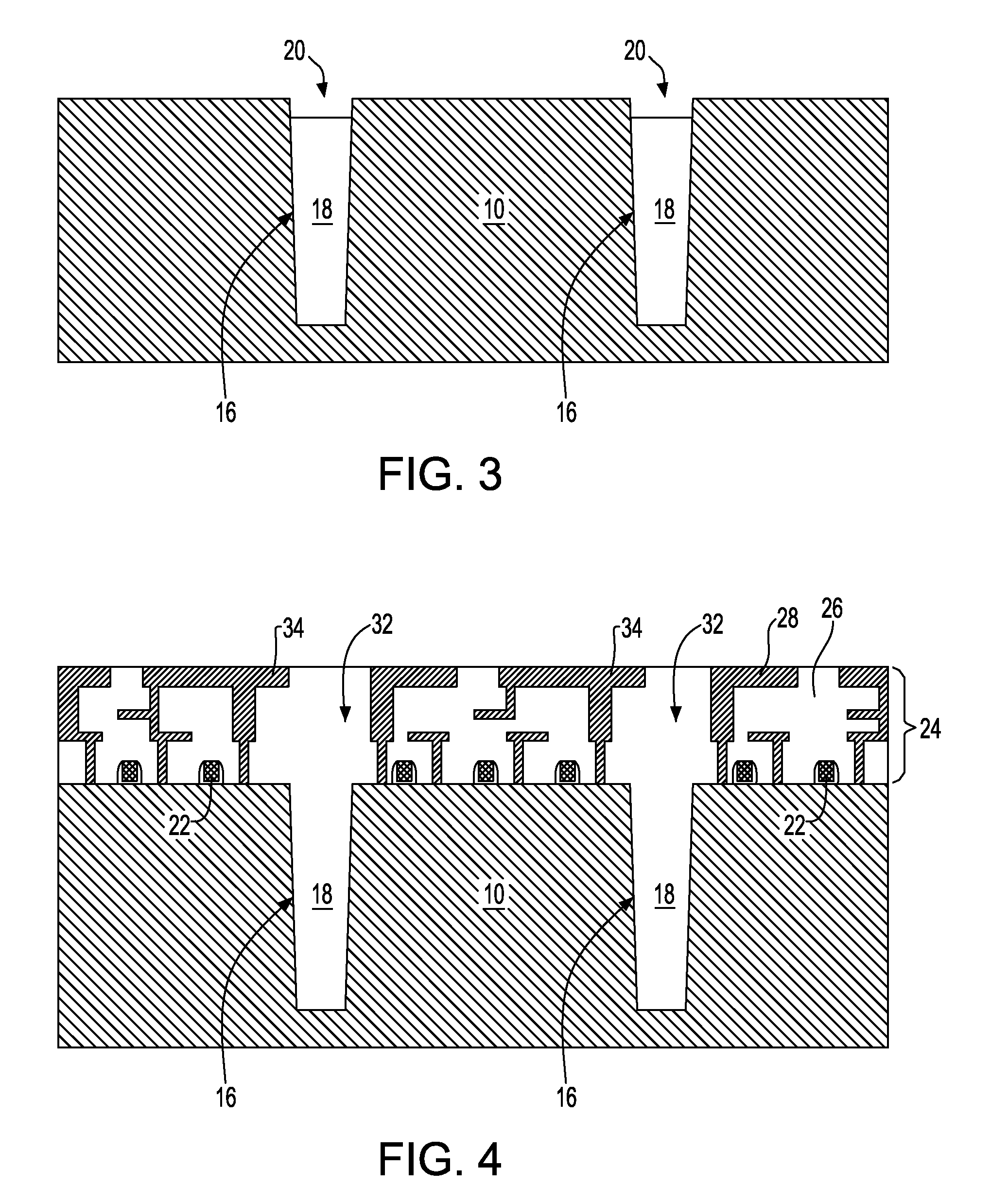
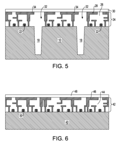
Method of making 3D integrated circuits and structures formed thereby
PatentActiveUS20100193964A1
Innovation
- A method involving forming trenches in semiconductor wafers, filling them with insulators, aligning and bonding wafers, etching to expose pads, and filling the trenches with electrical conductors to create through silicon vias that connect integrated circuits, optimizing connectivity and reducing wire length.
Material Science Advancements Supporting Twistronics
The advancement of material science has been pivotal in enabling the practical implementation of twistronics for integrated circuit design. Two-dimensional (2D) materials, particularly graphene and transition metal dichalcogenides (TMDCs), have emerged as the foundation for twistronics applications. These atomically thin materials exhibit exceptional electronic properties when stacked at specific twist angles, creating moiré superlattices that dramatically alter their band structures.
Recent breakthroughs in chemical vapor deposition (CVD) techniques have significantly improved the quality and scalability of 2D material production. These advancements allow for the precise control of layer thickness, crystallinity, and defect density—critical factors for maintaining consistent electronic properties across large-area substrates required for commercial integrated circuit fabrication.
Hexagonal boron nitride (hBN) has proven to be an indispensable material in twistronics, serving as an ideal dielectric substrate and encapsulation layer. Its atomically smooth surface and lack of dangling bonds minimize interfacial scattering, preserving the intrinsic properties of the active 2D materials. Innovations in hBN synthesis have yielded larger crystal domains and improved thickness uniformity, addressing previous limitations in device scaling.
The development of specialized transfer techniques represents another crucial advancement. Dry transfer methods using polycarbonate or polydimethylsiloxane (PDMS) stamps now enable the placement of 2D materials with angular precision approaching 0.1 degrees—essential for achieving the desired moiré patterns that underpin twistronics phenomena.
Interfacial engineering has emerged as a key focus area, with researchers developing novel approaches to control the interlayer coupling strength. Methods such as intercalation of small molecules or ions between layers provide additional tuning mechanisms for electronic properties, expanding the design space for twistronics-based integrated circuits.
Advances in characterization techniques have been equally important. High-resolution transmission electron microscopy (HRTEM), scanning tunneling microscopy (STM), and angle-resolved photoemission spectroscopy (ARPES) now allow for direct visualization and measurement of moiré superlattices and their electronic structures, providing crucial feedback for material optimization.
Thermal management materials represent another critical advancement, as twistronics devices often operate under specific temperature conditions to maintain their unique electronic states. Novel thermal interface materials with high in-plane thermal conductivity but low cross-plane thermal conductivity help maintain temperature uniformity while allowing for efficient heat dissipation in densely packed circuits.
Quantum Computing Integration Possibilities
The integration of twistronics with quantum computing represents a frontier with transformative potential for integrated circuit design. Quantum computing systems, which leverage quantum mechanical phenomena to perform computations, could significantly benefit from the unique electronic properties that emerge in twisted 2D materials. The controlled manipulation of quantum states in twisted bilayer graphene and similar structures offers promising pathways for creating more stable qubits—the fundamental units of quantum information.
Twistronics-based materials exhibit properties that could address several critical challenges in quantum computing, particularly quantum decoherence and error correction. The tunable superconductivity in magic-angle twisted bilayer graphene might enable the development of novel superconducting qubits with enhanced coherence times. Additionally, the topological states that emerge in certain twisted configurations could potentially support topological quantum computing approaches, which are inherently more resistant to environmental noise.
From a fabrication perspective, the integration of twistronics into quantum computing architectures presents both opportunities and challenges. The precise angle control required for twistronics can be leveraged to create quantum gates with unprecedented precision. However, maintaining quantum coherence while interfacing with conventional electronic components remains a significant engineering challenge that requires innovative approaches to materials integration and signal isolation.
Recent experimental demonstrations have shown promising results in coupling twisted van der Waals heterostructures with superconducting quantum circuits. These hybrid systems could potentially serve as quantum transducers, facilitating the conversion between different types of quantum information carriers—such as between photonic and electronic qubits—which is essential for scalable quantum computing architectures.
The temperature dependence of twistronics phenomena also presents interesting possibilities for quantum computing. While many quantum computing platforms require extremely low temperatures to operate, certain twistronics-based systems exhibit quantum behaviors at relatively higher temperatures. This characteristic could potentially reduce the cooling requirements for certain quantum computing components, making quantum systems more practical for widespread deployment.
Looking forward, the convergence of twistronics and quantum computing could lead to entirely new paradigms in quantum information processing. Moiré superlattices might serve as quantum simulators for complex quantum systems that are otherwise computationally intractable, opening new avenues for quantum algorithm development and implementation in specialized integrated circuits.
Unlock deeper insights with Patsnap Eureka Quick Research — get a full tech report to explore trends and direct your research. Try now!
Generate Your Research Report Instantly with AI Agent
Supercharge your innovation with Patsnap Eureka AI Agent Platform!