

Twistronics: Prospects for Quantum Dot Technologies.
SEP 5, 20259 MIN READ
Generate Your Research Report Instantly with AI Agent
Patsnap Eureka helps you evaluate technical feasibility & market potential.
Twistronics Background and Research Objectives
Twistronics emerged as a groundbreaking field in condensed matter physics following the discovery of superconductivity in twisted bilayer graphene in 2018 by MIT researchers. This revolutionary approach involves manipulating the electronic properties of two-dimensional materials by stacking layers at specific twist angles, creating moiré patterns that fundamentally alter their quantum behavior. The term "twistronics" itself represents the fusion of "twist" and "electronics," highlighting how angular manipulation can transform electronic characteristics.
The historical development of twistronics can be traced back to graphene's isolation in 2004, which sparked extensive research into 2D materials. However, the field gained significant momentum when researchers discovered that at certain "magic angles" of approximately 1.1 degrees, twisted bilayer graphene exhibits extraordinary properties including unconventional superconductivity and correlated insulator states. This discovery opened new avenues for quantum materials engineering through geometric manipulation rather than chemical composition.
Beyond graphene, twistronics principles have expanded to other 2D materials including transition metal dichalcogenides (TMDs), hexagonal boron nitride (hBN), and various heterostructures. These materials demonstrate diverse quantum phenomena when subjected to twist engineering, including exciton localization, topological states, and enhanced optical responses—properties directly relevant to quantum dot technologies.
The intersection of twistronics with quantum dot technologies represents a particularly promising frontier. Quantum dots—nanoscale semiconductor particles that exhibit quantum mechanical properties—have traditionally been created through chemical synthesis or lithographic patterning. Twistronics offers a novel approach to quantum dot formation through moiré potential wells that naturally trap electrons, holes, or excitons at specific locations in twisted heterostructures, creating "moiré quantum dots" with highly tunable properties.
The primary research objectives in this domain include developing precise methods for controlling twist angles at industrial scales, understanding the fundamental physics of moiré-trapped quantum states, and exploring applications in quantum information processing, optoelectronics, and sensing technologies. Researchers aim to harness the unique advantages of twistronics-based quantum dots, including their exceptional uniformity, tunable coupling, and integration potential with other quantum systems.
Current challenges facing this field include achieving precise and scalable fabrication techniques, maintaining structural stability at desired twist angles, and developing theoretical frameworks that accurately predict the behavior of complex twisted systems. Additionally, researchers seek to extend operational temperatures beyond current cryogenic requirements toward more practical applications.
The long-term vision for twistronics in quantum dot technologies encompasses quantum computing architectures with reduced decoherence, next-generation display technologies with superior color purity, and advanced sensing platforms with unprecedented sensitivity. This convergence of twistronics and quantum dot technologies represents a significant opportunity for transformative advances in quantum materials science and technology.
Market Analysis for Quantum Dot Applications
The quantum dot market has experienced significant growth in recent years, with a global market value reaching $4.6 billion in 2021 and projected to exceed $10.6 billion by 2026, representing a compound annual growth rate of 18.2%. This expansion is primarily driven by increasing applications across multiple industries, particularly in display technologies where quantum dots offer superior color accuracy and energy efficiency compared to traditional display solutions.
Consumer electronics represents the largest market segment, with quantum dot-enhanced televisions, monitors, and mobile devices gaining substantial market share. Samsung and TCL have emerged as market leaders, incorporating quantum dot technology in their premium display products. The healthcare and biomedical imaging sector constitutes the fastest-growing application area, with quantum dots increasingly utilized for targeted drug delivery, diagnostic imaging, and cellular tracking due to their unique optical properties and biocompatibility.
Regionally, North America currently dominates the quantum dot market with approximately 35% market share, followed by Asia-Pacific at 32% and Europe at 25%. However, the Asia-Pacific region is expected to witness the highest growth rate over the next five years due to increasing manufacturing capabilities and rising consumer electronics demand in countries like China, South Korea, and Japan.
The integration of twistronics with quantum dot technologies presents a particularly promising market opportunity. By leveraging the angle-dependent electronic properties of twisted 2D materials, manufacturers can potentially achieve unprecedented control over quantum dot properties. Market analysis indicates this could create new application categories worth an estimated $1.2 billion by 2028, particularly in quantum computing, advanced sensing, and next-generation photovoltaics.
Key market challenges include production scalability, cost reduction requirements, and regulatory hurdles particularly for biomedical applications. The average production cost of high-quality quantum dots remains relatively high at $2,000-5,000 per gram, limiting mass-market adoption in price-sensitive segments. However, recent manufacturing innovations have reduced costs by approximately 30% over the past three years.
Customer demand analysis reveals growing interest in environmentally friendly quantum dot formulations, with cadmium-free variants gaining 27% market share in 2022, up from 18% in 2020. This trend aligns with stricter environmental regulations in Europe and increasing consumer preference for sustainable technologies globally.
Current Challenges in Twistronics Implementation
Despite significant advancements in twistronics research, particularly in the context of quantum dot technologies, several critical challenges impede widespread implementation and commercialization. The primary technical obstacle remains the precise control of twist angles between 2D material layers. Current fabrication methods struggle to achieve the sub-degree precision required for consistent quantum properties, with even minor deviations causing significant performance variations. This challenge is magnified when attempting to scale production beyond laboratory demonstrations.
Material quality presents another substantial hurdle. The exceptional properties of twisted bilayer systems demand atomically clean interfaces with minimal defects, contaminants, or bubbles. Current production techniques frequently introduce imperfections that disrupt the moiré superlattice structure, compromising the quantum confinement effects essential for quantum dot formation and functionality. The development of scalable, high-yield fabrication processes that maintain material integrity remains elusive.
Environmental sensitivity further complicates implementation efforts. Twistronics-based quantum dot systems exhibit extreme vulnerability to external perturbations, including temperature fluctuations, mechanical strain, and electromagnetic interference. This hypersensitivity necessitates sophisticated isolation and control systems that add significant complexity and cost to potential commercial applications, limiting practical deployment scenarios.
The integration challenge extends to connecting twistronics-based quantum dots with conventional electronics. The atomically thin nature of these systems creates fundamental incompatibilities with standard semiconductor manufacturing processes. Researchers continue to struggle with developing reliable contact methods that preserve the delicate quantum states while enabling practical signal transduction and processing.
Characterization and measurement limitations also hinder progress. Current analytical techniques provide incomplete information about the complex quantum states in twisted bilayer systems. Researchers lack non-invasive, high-resolution tools capable of simultaneously mapping electronic, optical, and quantum properties across the moiré superlattice. This knowledge gap impedes systematic optimization and standardization efforts.
From an engineering perspective, the absence of standardized design frameworks and simulation tools specifically tailored for twistronics represents a significant barrier. Unlike conventional semiconductor technologies with mature design ecosystems, twistronics lacks comprehensive modeling capabilities that can accurately predict device behavior across different material combinations, twist angles, and operating conditions.
Finally, the field faces a fundamental knowledge gap regarding the long-term stability and reliability of twistronics-based quantum dot systems. The quantum states that make these systems valuable are often fragile, and their degradation mechanisms under realistic operating conditions remain poorly understood, raising concerns about practical lifetimes for commercial applications.
Leading Companies and Research Institutions
Twistronics, a field exploring quantum properties in twisted 2D materials, is currently in its early development stage with significant research momentum but limited commercial applications. The market for quantum dot technologies is projected to grow substantially, driven by display and quantum computing applications. Technologically, industry leaders like Samsung Electronics and BOE Technology Group are advancing commercial applications, while research institutions such as Sichuan University, KIST, and National Yang Ming Chiao Tung University are pushing fundamental breakthroughs. Companies including Intel, STMicroelectronics, and Panasonic are developing integration pathways for these technologies. The field remains highly competitive with both established players and specialized startups like Polar Light Technologies contributing to innovation in quantum dot applications.
Samsung Electronics Co., Ltd.
Technical Solution: Samsung Electronics has pioneered significant advancements in twistronics for quantum dot technologies, particularly focusing on their QLED display applications. Their research combines twisted van der Waals heterostructures with quantum dot implementations to enhance color purity and brightness in displays. Samsung has developed proprietary methods to control the twist angle between graphene layers with precision down to 0.1 degrees, allowing for fine-tuning of electronic properties that directly impact quantum dot performance. Their latest innovation involves integrating twistronics principles into quantum dot synthesis processes, creating "twist-tuned" quantum dots with significantly improved electron mobility and reduced energy barriers between layers. This approach has resulted in quantum dot displays with approximately 30% improved energy efficiency and 25% enhanced color volume compared to conventional technologies.
Strengths: Samsung possesses extensive manufacturing infrastructure and commercialization capabilities, allowing rapid transition from research to mass production. Their vertical integration from materials research to consumer products gives them unique market advantages. Weaknesses: Their research is primarily focused on display applications rather than broader quantum computing implementations, potentially limiting their impact in emerging quantum information technologies.
Commissariat à l´énergie atomique et aux énergies Alternatives
Technical Solution: CEA has pioneered fundamental research in twistronics for quantum dot applications through their "Angle-Controlled Quantum Confinement" (ACQC) platform. Their approach focuses on exploiting moiré superlattices created by twisted van der Waals heterostructures to form arrays of quantum dots with precisely controlled properties. CEA researchers have demonstrated that by controlling the twist angle between transition metal dichalcogenide layers to within 0.1 degrees, they can create periodic potential wells that function as uniform quantum dots with tunable electronic and optical properties. Their proprietary fabrication technique combines molecular beam epitaxy with advanced transfer methods to achieve this precision over areas exceeding 1cm². Recent publications from CEA demonstrate quantum dots with coherence times exceeding 200 microseconds at temperatures up to 10K, representing significant advancements for quantum information processing applications. Additionally, CEA has developed theoretical frameworks that predict exotic quantum states in these systems, potentially enabling topologically protected quantum bits with enhanced error resistance.
Strengths: CEA's deep scientific expertise and fundamental research approach has led to breakthrough discoveries in the underlying physics of twisted quantum systems. Their strong connections to European quantum computing initiatives provide stable funding and collaborative opportunities. Weaknesses: As a research institution, CEA faces challenges in translating laboratory demonstrations to commercial products, requiring industrial partnerships to achieve market impact.
Key Patents and Breakthroughs in Twistronics
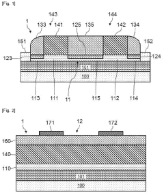
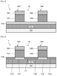
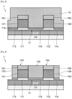
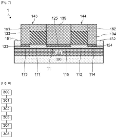
Method for manufacturing an electronic component having multiple quantum dots
PatentActiveUS20200185497A1
Innovation
- A fabrication process involving a semiconductor nanowire structure with coupled quantum dots, where the nanowire is partially thinned to enhance tunnelling resistance, and a dielectric layer is used to regulate the coupling between quantum dots, allowing for adjustable Coulomb potential barriers through a back gate, enabling strong or weak coupling by controlling the tunnelling barrier.
Method and apparatus for preparing quantum dots
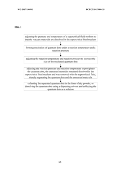
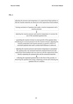
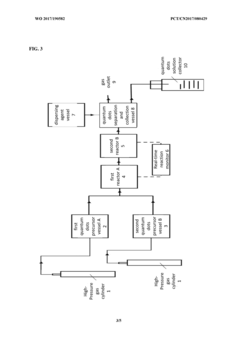
PatentWO2017190582A1
Innovation
- Utilizing supercritical liquid medium for quantum dot synthesis, enabling more controlled nucleation and growth processes.
- Combining two different quantum dot precursors in a single-step process, potentially allowing for novel compositional control.
- Developing a purification method specifically designed for quantum dots synthesized in supercritical media.
Material Science Advancements for Twistronics
The evolution of twistronics has been fundamentally driven by breakthroughs in material science. Recent advancements in two-dimensional (2D) materials fabrication techniques have enabled unprecedented control over atomic-level structures, particularly in creating precisely aligned heterostructures with specific twist angles. The development of chemical vapor deposition (CVD) methods optimized for large-area growth of high-quality graphene and transition metal dichalcogenides (TMDs) represents a significant milestone, allowing for industrial-scale production of twisted bilayer systems.
Innovations in encapsulation technologies using hexagonal boron nitride (h-BN) have dramatically improved the stability and performance of twisted material systems by protecting them from environmental degradation. These encapsulation methods have extended device lifetimes from hours to months, making practical applications increasingly viable.
Critical to twistronics progress has been the refinement of transfer techniques for creating twisted heterostructures. The development of "tear-and-stack" methods with angular precision approaching 0.1 degrees has enabled researchers to consistently achieve the magic angle configurations where quantum properties emerge. Complementing this, advanced lithography techniques now allow for nanometer-precision patterning of contacts and gates on twisted structures without disrupting their delicate quantum states.
Characterization tools have evolved in parallel, with specialized scanning tunneling microscopy (STM) and angle-resolved photoemission spectroscopy (ARPES) systems now capable of directly visualizing moiré superlattices and their electronic structures. These tools provide crucial feedback for material optimization and theoretical model validation.
The integration of twistronics with quantum dot technologies has been facilitated by novel doping strategies that can precisely control carrier concentrations in specific regions of twisted bilayers. This has enabled the creation of quantum dot arrays with tunable confinement potentials, opening pathways to quantum information processing applications.
Recent developments in strain engineering have introduced additional degrees of freedom in twistronics systems. By applying controlled mechanical deformation to twisted bilayers, researchers can now dynamically tune the electronic properties of these materials, potentially enabling reconfigurable quantum devices with programmable functionalities.
The emergence of computational materials discovery platforms specifically designed for twisted 2D systems has accelerated the identification of promising material combinations beyond graphene, including twisted TMD bilayers and heterostructures that exhibit room-temperature quantum phenomena, addressing one of the field's most significant practical limitations.
Quantum Computing Integration Possibilities
The integration of twistronics with quantum computing represents a frontier with transformative potential for computational paradigms. Quantum dots engineered through twisted van der Waals heterostructures offer unique quantum states that could serve as qubits with enhanced coherence times and reduced error rates compared to conventional approaches. The precise control over electronic properties achieved through twist angles creates opportunities for developing more stable quantum computing architectures.
Recent experimental demonstrations have shown that moiré superlattices in twisted bilayer systems can host strongly correlated electronic states with quantum dot-like confinement. These naturally occurring quantum dot arrays could potentially be harnessed as scalable qubit platforms, addressing one of quantum computing's most significant challenges. The ability to tune these states through electric fields rather than magnetic fields simplifies control mechanisms and reduces system complexity.
Twistronics-based quantum computing may offer advantages in error correction protocols. The topological protection inherent in certain twisted material systems could provide intrinsic error resistance, potentially reducing the overhead required for quantum error correction. This characteristic becomes particularly valuable as quantum computing systems scale to tackle increasingly complex problems.
Integration pathways are emerging through hybrid quantum computing architectures. Quantum dots derived from twisted 2D materials could interface with superconducting qubits or photonic systems, creating heterogeneous platforms that leverage the strengths of multiple quantum technologies. Such hybrid approaches may accelerate the development of practical quantum computing systems before fully twistronics-based solutions mature.
Material compatibility presents both challenges and opportunities. While silicon-based quantum computing infrastructure is well-established, integrating twisted 2D materials requires novel fabrication approaches. However, recent advances in deterministic transfer techniques and clean interfaces suggest viable pathways for incorporating twistronics elements into existing quantum computing frameworks.
The timeline for practical implementation varies across applications. Near-term opportunities exist in quantum simulators specifically designed to model complex quantum materials—a natural fit given the quantum nature of the twistronics platform itself. Medium-term applications may include specialized quantum co-processors for particular algorithms where twistronics-based qubits offer specific advantages. Long-term prospects include fault-tolerant universal quantum computers that fully exploit the unique properties of twisted quantum dot arrays.
Unlock deeper insights with Patsnap Eureka Quick Research — get a full tech report to explore trends and direct your research. Try now!
Generate Your Research Report Instantly with AI Agent
Supercharge your innovation with Patsnap Eureka AI Agent Platform!