The Role of Twistronics in Next-Gen Wireless Communication Systems.
SEP 5, 202510 MIN READ
Generate Your Research Report Instantly with AI Agent
Patsnap Eureka helps you evaluate technical feasibility & market potential.
Twistronics Background and Communication Goals
Twistronics represents a revolutionary field in materials science that emerged prominently after the groundbreaking discovery of superconductivity in twisted bilayer graphene in 2018. This phenomenon occurs when two-dimensional materials are stacked with a slight rotational misalignment, creating a moiré pattern that fundamentally alters the electronic properties of the composite material. The angular precision in these twisted structures enables unprecedented control over quantum properties, including conductivity, magnetic response, and optical characteristics.
The historical development of twistronics can be traced back to theoretical predictions in the early 2010s, but experimental validation only became possible with advances in nanofabrication techniques that allowed precise control of twist angles between atomic layers. This technological evolution has opened new avenues for manipulating electromagnetic waves at the quantum level, presenting transformative possibilities for wireless communication systems.
Current wireless communication technologies face significant challenges including spectrum scarcity, energy efficiency limitations, and physical constraints on data transmission rates. Twistronics offers potential solutions by enabling novel materials with tunable electromagnetic properties that could revolutionize how signals are generated, transmitted, and received. The quantum behaviors exhibited by twisted materials suggest possibilities for developing components that operate at higher frequencies with greater efficiency than conventional technologies.
The primary technical goals for twistronics in next-generation wireless communications include developing tunable materials for adaptive frequency operation, creating ultra-efficient signal processing components, and establishing quantum-enhanced secure communication channels. These objectives align with the broader industry trajectory toward 6G and beyond, where communication systems will require unprecedented bandwidth, minimal latency, and maximum energy efficiency.
Research indicates that twisted van der Waals heterostructures could potentially enable terahertz-range communications, which would dramatically expand available bandwidth compared to current systems. Additionally, the unique quantum properties of these materials may facilitate novel modulation techniques that increase spectral efficiency by orders of magnitude.
The convergence of twistronics with other emerging technologies such as metamaterials, photonics, and quantum computing creates a rich innovation landscape. This interdisciplinary approach is essential for addressing the complex challenges of future communication systems that will need to support exponentially growing data demands while reducing energy consumption.
As the field progresses, researchers are exploring increasingly sophisticated multi-layer structures with precisely engineered twist angles to achieve specific electromagnetic properties tailored for communication applications. The ultimate goal is to develop a new generation of communication infrastructure that transcends the limitations of conventional electronics, enabling truly ubiquitous, high-capacity wireless connectivity.
Market Demand Analysis for Twistronics-Based Wireless Systems
The global wireless communication market is experiencing unprecedented growth, with the demand for faster, more reliable, and energy-efficient systems reaching critical levels. Twistronics, the science of manipulating the electronic properties of 2D materials by adjusting the twist angle between layers, presents a promising frontier for addressing these escalating market needs. Current market projections indicate that the 6G wireless communication market, where twistronics could play a pivotal role, is expected to grow significantly through 2030 and beyond.
The primary market drivers for twistronics-based wireless systems stem from several converging factors. First, data consumption continues to increase exponentially, with global mobile data traffic projected to reach zettabyte levels by 2025. Traditional semiconductor technologies are approaching their physical limitations in meeting these demands, creating a technological gap that twistronics could potentially fill.
Enterprise and industrial sectors represent the most immediate market opportunity for twistronics applications. These sectors require ultra-reliable low-latency communication (URLLC) for applications such as industrial automation, remote surgery, and autonomous vehicle networks. The unique properties of twisted bilayer graphene and other 2D materials could enable the development of components capable of operating at terahertz frequencies with unprecedented efficiency.
Consumer markets also present substantial growth potential, particularly as augmented reality, virtual reality, and metaverse applications gain mainstream adoption. These applications demand extremely high bandwidth and minimal latency, requirements that current 5G technology struggles to fully satisfy. Market research indicates that consumers are increasingly willing to pay premium prices for devices offering tangible improvements in connectivity performance.
Geographically, the most robust initial demand for twistronics-based wireless systems is expected in technology-forward regions with dense urban populations, including East Asia, North America, and Western Europe. These markets combine high consumer purchasing power with advanced infrastructure capable of supporting next-generation wireless technologies.
Defense and aerospace sectors represent another significant market segment, with particular interest in the radiation-hardened properties and potential security advantages of twistronics-based communication systems. Government investment in these technologies is expected to provide substantial early-stage market support while consumer applications mature.
The market timing appears favorable for twistronics integration into wireless systems, as the industry is currently in the early planning stages for 6G technology, with standardization expected to begin around 2025-2026. This timeline aligns well with the projected development curve for practical twistronics applications, potentially allowing for strategic positioning of this technology within the emerging 6G ecosystem.
Current State and Challenges in Twistronics Implementation
Twistronics, a field that emerged from the discovery of superconductivity in twisted bilayer graphene in 2018, has made significant strides in theoretical understanding but faces substantial implementation challenges for wireless communication applications. Currently, laboratory demonstrations have successfully shown how the precise control of twist angles between 2D material layers can create moiré patterns that dramatically alter electronic properties, potentially enabling novel high-frequency signal processing capabilities essential for next-generation wireless systems.
The global research landscape shows concentrated efforts in leading institutions across North America, Europe, and East Asia, with the United States and China dominating patent filings related to twistronics applications in communications. Recent breakthroughs include the development of tunable terahertz emitters using twisted van der Waals heterostructures and the demonstration of programmable electromagnetic wave manipulation through dynamic twist angle modulation.
Despite these advances, several critical challenges impede practical implementation. Foremost is the scalability barrier—current fabrication techniques for precisely twisted structures remain largely artisanal, limited to micrometer-scale samples unsuitable for commercial deployment. The "twist angle precision problem" represents another significant hurdle, as even sub-degree variations can dramatically alter the desired electronic properties, necessitating unprecedented manufacturing precision at scale.
Stability and reliability issues also plague current implementations, with environmental factors such as temperature fluctuations and mechanical stress causing twist angle drift over time. This instability compromises the long-term performance consistency required for telecommunications infrastructure. Additionally, integration challenges with existing CMOS technology create compatibility barriers that must be overcome before twistronics can be incorporated into conventional wireless communication systems.
Energy efficiency represents another critical concern, as current twistronics-based devices require sophisticated cooling systems to maintain optimal performance, making them impractical for energy-constrained applications like mobile devices or IoT nodes. The cost factor further compounds implementation difficulties, with current fabrication methods involving expensive equipment and low yields, resulting in prohibitive costs for mass production.
From a geographical perspective, research capabilities are unevenly distributed, with advanced fabrication facilities concentrated in a handful of countries, creating potential supply chain vulnerabilities for global adoption. Regulatory uncertainties regarding novel materials and potential environmental impacts of large-scale production also present non-technical barriers to implementation that must be addressed through international standards development and safety assessments.
Key Industry Players in Twistronics Research and Development
Twistronics in next-generation wireless communication systems is emerging as a transformative technology, currently in the early development stage with growing market potential. The competitive landscape features major players like Qualcomm, Samsung, and Huawei Digital Power leading commercial applications, while research institutions such as the University of California and Xidian University drive fundamental innovation. Telecommunications giants including Ericsson, ZTE, and NTT Docomo are integrating twistronics into their wireless infrastructure solutions. The technology is approaching commercial viability with semiconductor companies like Intel and electronics manufacturers such as LG and Sony developing practical implementations, though widespread deployment remains 3-5 years away as technical challenges are addressed.
Samsung Electronics Co., Ltd.
Technical Solution: Samsung Electronics has developed an extensive twistronics program focused on next-generation wireless communications through their Advanced Communications Research Center. Their approach centers on what they call "Programmable Electromagnetic Surfaces" (PES) using twisted van der Waals heterostructures. Samsung's technology utilizes precisely controlled twist angles between layers of graphene and hexagonal boron nitride (hBN) to create reconfigurable electromagnetic properties that can be dynamically tuned through electrical gating. This enables adaptive beamforming, frequency-agile operation, and intelligent interference management without mechanical components. Samsung has demonstrated prototype systems operating in the 28 GHz and 39 GHz bands with beam steering capabilities exceeding 60 degrees and switching speeds under 100 nanoseconds. Their fabrication techniques have achieved twist angle uniformity across 200mm wafers, addressing a key manufacturing challenge. Samsung has integrated these twistronics-based components with their existing semiconductor technology to create hybrid systems that leverage the strengths of both conventional and quantum materials, with particular focus on energy efficiency for mobile devices and small cells.
Strengths: Vertical integration capabilities from materials research through device manufacturing to system deployment, with substantial resources for commercialization. Their hybrid approach allows for incremental adoption of twistronics technology. Weaknesses: The complex materials systems require specialized manufacturing processes that may be difficult to scale economically, and the technology faces competition from alternative approaches within Samsung's diverse R&D portfolio.
The Regents of the University of California
Technical Solution: The University of California system has been at the forefront of twistronics research since the field's inception, with groundbreaking work emerging from UC Berkeley, UCLA, and UCSD. Their approach to wireless communications leverages moiré superlattices created by stacking and twisting 2D materials at specific angles. UC researchers have developed novel tunable RF filters using twisted bilayer graphene that can dynamically adjust their frequency response through electrical gating, eliminating the need for multiple fixed filters in multi-band communication systems. Their published research demonstrates THz-frequency modulators with modulation depths exceeding 70% using graphene/hBN twisted heterostructures, significantly outperforming conventional semiconductor technologies. Additionally, UC labs have pioneered methods for large-area fabrication of twisted 2D materials with controlled domain sizes exceeding 100 μm², addressing a critical manufacturing challenge. Recent work has focused on integrating these materials with CMOS technology to create hybrid communication systems that combine the advantages of conventional electronics with the unique properties of twisted 2D materials.
Strengths: World-leading fundamental research capabilities with extensive intellectual property in twistronics. Their academic approach has yielded breakthrough discoveries with significant potential for commercialization. Weaknesses: As an academic institution, they face challenges in translating laboratory discoveries to commercial-scale manufacturing and may require industry partnerships to fully realize the technology's potential.
Core Patents and Breakthroughs in Twistronics Communication
Narrowband diagnostics of twisted pair wiring
PatentWO2010091379A1
Innovation
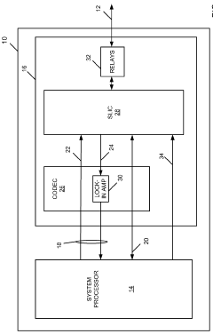
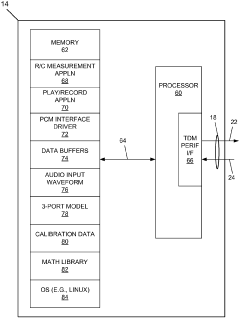
- A system comprising a Subscriber Line Interface Circuit (SLIC), a codec, and a system processor that transmits sinusoidal signals onto twisted pair wiring, senses current, and determines resistance and capacitance using a lock-in amplifier to filter out noise and measure electrical properties accurately.


Methods and apparatus for forming cable media
PatentInactiveUS20060059883A1
Innovation
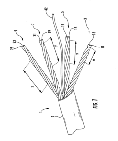
- The method involves forming cabling media with twisted wire pairs that have varying twist lengths, achieved through a pretwist modulation using a wire pair twist modulator and additional twisting by a wire pair twisting device, to reduce crosstalk and enhance operational performance.
Spectrum Efficiency and Bandwidth Enhancement Potential
Twistronics offers unprecedented opportunities for enhancing spectrum efficiency and bandwidth in next-generation wireless communication systems. The manipulation of twisted layers in 2D materials creates unique electronic properties that can be harnessed to address the growing bandwidth demands of modern telecommunications. Current wireless systems face significant spectrum congestion, with traditional frequency bands becoming increasingly saturated as device proliferation continues exponentially.
The moiré superlattices formed in twisted bilayer graphene and similar materials demonstrate remarkable tunable electronic properties that can be leveraged for signal modulation and processing. Research indicates that twistronics-based devices could potentially achieve modulation densities up to 10-100 times greater than conventional semiconductor technologies, enabling more efficient use of available spectrum resources.
Bandwidth enhancement through twistronics manifests in several key mechanisms. First, the angle-dependent electronic properties allow for dynamic frequency tuning without additional hardware components, creating opportunities for adaptive spectrum utilization. This capability enables communication systems to respond in real-time to changing network conditions and bandwidth requirements.
Furthermore, the quantum properties of twisted materials facilitate novel multiplexing techniques beyond traditional approaches. Preliminary experiments have demonstrated that twistronics-based transceivers can simultaneously process multiple data streams across overlapping frequency bands with minimal interference, effectively increasing channel capacity without expanding spectrum allocation.
The non-linear response characteristics of twisted bilayer systems also show promise for bandwidth expansion through harmonic generation and frequency mixing. These properties enable efficient frequency conversion and the utilization of previously inaccessible portions of the electromagnetic spectrum, particularly in the terahertz range which remains largely untapped for commercial communications.
Recent theoretical models suggest that optimally designed twistronics-based communication systems could achieve spectral efficiencies approaching the Shannon limit more closely than existing technologies. This is particularly significant for millimeter-wave and sub-terahertz communications, where conventional approaches struggle with signal propagation and energy efficiency challenges.
Implementation challenges remain, particularly in maintaining precise twist angles under varying environmental conditions and scaling production for commercial deployment. However, recent advances in fabrication techniques, including self-assembly methods and automated twist-angle control systems, suggest these hurdles may be overcome within the next 3-5 years.
The potential impact on wireless infrastructure is substantial, with twistronics potentially enabling the equivalent of multiple generations of bandwidth improvement in a single technological leap. This would address critical capacity constraints in urban environments and enable new applications requiring ultra-high bandwidth, including holographic communications and immersive extended reality experiences.
Material Science Advancements Supporting Twistronics
The advancement of twistronics fundamentally relies on breakthroughs in material science. Recent developments in two-dimensional (2D) materials have created the foundation for twistronics, with graphene being the pioneering material. The precise control of atomic layers with specific twist angles between them has enabled the creation of moiré superlattices with unique electronic properties.
Significant progress has been made in fabrication techniques that allow for atomic-level precision in creating twisted heterostructures. These include dry transfer methods with rotational control, which have evolved from manual approaches to automated systems capable of achieving angular precision below 0.1 degrees. This precision is critical for accessing the "magic angles" where electronic properties dramatically change.
Beyond graphene, the material palette for twistronics has expanded to include transition metal dichalcogenides (TMDs), hexagonal boron nitride (hBN), and various van der Waals heterostructures. Each material combination offers distinct electronic, optical, and magnetic properties that can be engineered through twist angle manipulation.
Characterization technologies have also evolved to support twistronics research. Advanced microscopy techniques such as scanning tunneling microscopy (STM) and transmission electron microscopy (TEM) now allow researchers to visualize moiré patterns and confirm structural configurations at the atomic scale. Angle-resolved photoemission spectroscopy (ARPES) has become instrumental in mapping the electronic band structures of twisted materials.
Material stability and defect control represent ongoing challenges. Researchers have developed encapsulation methods using hBN to protect sensitive twisted structures from environmental degradation. Additionally, new approaches to minimize strain and ensure uniform twist angles across larger areas are emerging, which is essential for scaling up twistronics for practical applications.
For wireless communication applications specifically, materials research has focused on enhancing properties relevant to high-frequency operation. This includes developing twisted structures with tunable conductivity, low loss tangents, and high carrier mobility. Recent experiments with twisted bilayer graphene have demonstrated terahertz frequency response that can be electrically controlled, suggesting potential for reconfigurable RF components.
The integration of twistronics with conventional semiconductor platforms represents another frontier in materials science. Hybrid approaches combining twisted 2D materials with silicon or III-V compounds are being explored to leverage the strengths of both material systems while addressing fabrication compatibility challenges.
Unlock deeper insights with Patsnap Eureka Quick Research — get a full tech report to explore trends and direct your research. Try now!
Generate Your Research Report Instantly with AI Agent
Supercharge your innovation with Patsnap Eureka AI Agent Platform!