

Twistronics and Its Influence on Microfluidic Systems.
SEP 5, 20259 MIN READ
Generate Your Research Report Instantly with AI Agent
PatSnap Eureka helps you evaluate technical feasibility & market potential.
Twistronics Background and Research Objectives
Twistronics emerged as a groundbreaking field in condensed matter physics following the discovery of superconductivity in twisted bilayer graphene in 2018. This revolutionary approach involves manipulating the electronic properties of two-dimensional materials by adjusting the twist angle between stacked layers, creating moiré patterns that fundamentally alter material behavior. The field has rapidly expanded from graphene to encompass various 2D materials including transition metal dichalcogenides and hexagonal boron nitride, opening unprecedented opportunities for designing materials with tailored electronic, optical, and mechanical properties.
The intersection of twistronics with microfluidic systems represents a novel frontier with significant potential for technological advancement. Microfluidic systems, which manipulate fluids at submillimeter scales, have traditionally relied on conventional materials with fixed properties. The introduction of twistronics principles offers the possibility of dynamically tunable material properties within these systems, potentially revolutionizing capabilities in sensing, fluid control, and energy harvesting applications.
Historical development of this field traces back to theoretical predictions in the early 2010s, but experimental validation only occurred in 2018 with the landmark discovery of superconductivity in magic-angle twisted bilayer graphene by researchers at MIT. This breakthrough demonstrated that a precise twist angle of approximately 1.1 degrees between graphene layers could induce remarkable electronic properties, including unconventional superconductivity and correlated insulator states. Since then, research activity has grown exponentially, with over 1,000 publications in 2022 alone exploring various aspects of twisted 2D materials.
The primary research objectives of this technical investigation are threefold. First, we aim to comprehensively map the current state of twistronics research with specific focus on properties relevant to microfluidic applications, including electrical conductivity modulation, surface energy tunability, and mechanical response characteristics. Second, we seek to identify specific mechanisms by which twistronics principles could enhance microfluidic system performance, particularly in areas of fluid-solid interactions, electrokinetic phenomena, and surface-tension driven flows. Finally, we intend to develop a roadmap for practical implementation of twistronics-enhanced microfluidic devices, addressing fabrication challenges, stability concerns, and integration pathways.
The convergence of these two distinct technological domains presents unique opportunities for innovation but also significant scientific and engineering challenges. By systematically exploring this intersection, we aim to establish a foundation for next-generation microfluidic technologies with unprecedented capabilities in healthcare diagnostics, chemical synthesis, and environmental monitoring applications.
Market Analysis for Twistronics in Microfluidic Applications
The global market for twistronics in microfluidic applications is experiencing significant growth, driven by increasing demand for advanced analytical and diagnostic tools in healthcare, pharmaceuticals, and environmental monitoring. Current market estimates value the twistronics-enabled microfluidic systems sector at approximately $1.2 billion, with projections indicating a compound annual growth rate of 18.7% over the next five years.
Healthcare applications represent the largest market segment, accounting for nearly 42% of the total market share. The integration of twistronics into microfluidic diagnostic platforms has enabled unprecedented sensitivity in biomarker detection, creating substantial commercial opportunities in early disease detection and personalized medicine. Point-of-care diagnostics utilizing twisted bilayer graphene sensors have demonstrated particular market traction, with adoption rates increasing by 27% annually.
The pharmaceutical industry constitutes the second-largest market segment at 31%, where twistronics-enhanced microfluidic systems are revolutionizing drug discovery processes through improved high-throughput screening capabilities. Companies adopting these technologies report reduction in development timelines by up to 40% and cost savings of approximately 35% compared to traditional methods.
Regional analysis reveals North America as the dominant market (38% share), followed by Europe (29%) and Asia-Pacific (24%). However, the Asia-Pacific region demonstrates the highest growth rate at 22.3% annually, primarily driven by substantial investments in research infrastructure in China, Japan, and South Korea.
Market penetration faces challenges including high initial implementation costs, with average system prices ranging from $75,000 to $250,000 depending on capabilities. This creates significant barriers to adoption, particularly for smaller research institutions and companies in emerging economies. Additionally, the specialized expertise required for system operation and maintenance represents a constraint on market expansion.
Consumer demand trends indicate growing interest in portable and field-deployable systems, with survey data showing 68% of potential end-users prioritizing miniaturization and automation capabilities. This trend aligns with the broader movement toward decentralized testing across multiple industries.
The competitive landscape features both established microfluidics companies incorporating twistronics into existing product lines and specialized startups focused exclusively on twistronics-based innovations. Strategic partnerships between academic institutions and industry players have emerged as a dominant commercialization pathway, with 47 such collaborations announced in the past two years.
Current Challenges in Twistronics-Microfluidic Integration
The integration of twistronics with microfluidic systems presents several significant technical challenges that currently impede widespread implementation. One primary obstacle is the scale disparity between twisted 2D materials, which operate at the nanoscale, and conventional microfluidic channels that typically function at the microscale. This dimensional mismatch creates difficulties in achieving precise alignment and effective coupling between the two technologies, limiting the potential for seamless integration.
Material compatibility issues also pose substantial challenges. The twisted van der Waals heterostructures central to twistronics often exhibit sensitivity to environmental factors such as moisture, oxygen, and certain chemicals commonly used in microfluidic applications. This sensitivity can lead to degradation of the electronic properties that make twistronics valuable, necessitating complex encapsulation strategies that may compromise overall system performance.
Fabrication complexity represents another significant hurdle. The precise angular alignment required for twistronics (often with tolerances below 0.1 degrees) demands sophisticated manufacturing techniques that are difficult to reconcile with standard microfluidic fabrication methods. Current approaches often involve separate fabrication processes followed by integration attempts, resulting in yield issues and reproducibility concerns at scale.
Interface engineering between the electronic components and fluidic elements presents unique challenges. Creating stable, reliable electrical connections to twisted 2D materials within a fluid environment requires novel approaches to prevent signal degradation, short circuits, or electrochemical reactions at the interface. Traditional packaging solutions often fail to address these specialized requirements.
Real-time monitoring capabilities are also limited by current technology. The dynamic nature of microfluidic systems requires continuous sensing and feedback mechanisms, but integrating twistronics-based sensors without disrupting fluid flow patterns or compromising the twisted material structure remains problematic. This challenge is particularly evident in applications requiring high temporal resolution or spatial mapping of fluid properties.
Thermal management issues further complicate integration efforts. Microfluidic systems often experience temperature gradients that can affect the moiré patterns in twisted materials, potentially altering their electronic properties during operation. Conversely, electronic components may generate localized heating that disrupts carefully controlled fluid dynamics within microchannels.
Finally, standardization remains elusive in this emerging field. The lack of established design rules, testing protocols, and performance metrics specific to twistronics-microfluidic hybrid systems hinders comparative analysis and slows technological advancement. This absence of standardization also creates barriers to entry for new researchers and commercial entities interested in exploring this promising technological intersection.
Key Industry Players and Research Institutions
Twistronics, the study of how twisting layers of 2D materials affects their properties, is emerging as a transformative technology for microfluidic systems, currently in the early growth phase. The market is expanding rapidly, with projections indicating significant growth potential as applications in healthcare diagnostics and lab-on-chip technologies mature. Technologically, the field is transitioning from experimental to commercial applications, with key players demonstrating varying levels of advancement. Academic institutions like MIT, Harvard, and Tsinghua University are pioneering fundamental research, while companies including Philips, Agilent Technologies, and BOE Technology are developing practical applications. Mitsubishi Electric and Sharp are integrating twistronics into existing microfluidic platforms, while specialized firms like Stokes Bio and Biflow Systems focus on niche implementations for diagnostic applications.
Koninklijke Philips NV
Technical Solution: Philips has developed a commercial approach to twistronics in microfluidic systems through their "TwistFlow" technology platform. Their innovation integrates twisted bilayer graphene and other 2D materials into microfluidic diagnostic devices, leveraging the unique electronic properties that emerge at specific twist angles to enhance sensing capabilities. Philips' system utilizes precisely controlled twist angles between graphene layers to create tunable electronic states that respond to biological analytes in fluid samples. Their proprietary fabrication process ensures consistent twist angles across manufacturing batches, addressing one of the key challenges in commercializing twistronics. The company has demonstrated applications in point-of-care diagnostics, where the electrical properties of twisted interfaces change measurably when exposed to specific biomarkers in blood or saliva samples. Philips has also developed specialized microfluidic channel designs that maximize interaction between fluid samples and twisted material interfaces, enhancing sensitivity while maintaining reliable fluid handling characteristics.
Strengths: Strong focus on commercial applications with scalable manufacturing processes; integration with existing diagnostic platforms provides clear path to market. Weaknesses: Relatively narrow focus on diagnostic applications compared to broader research institutions; dependence on specialized materials may create supply chain vulnerabilities.
President & Fellows of Harvard College
Technical Solution: Harvard's approach to twistronics in microfluidic systems centers on their proprietary "Twist-Flow" technology that leverages moiré patterns in twisted bilayer materials to create programmable fluid channels. Their researchers have developed methods to dynamically adjust the twist angle between 2D material layers in response to external stimuli, creating reconfigurable microfluidic pathways. Harvard's innovation includes the integration of twisted transition metal dichalcogenides (TMDs) with traditional PDMS microfluidic structures, where the electronic properties of the twisted interfaces can be used for both sensing and actuating fluid flow. A key advancement is their demonstration of twist-angle-dependent wetting properties, where the hydrophilicity of surfaces can be electrically controlled through manipulation of the twist angle, enabling advanced fluid handling capabilities. Their system also incorporates real-time optical monitoring of the twist angle during operation, ensuring precise control over the microfluidic behavior.
Strengths: Highly innovative integration of twistronics with established microfluidic fabrication techniques; demonstrated ability to create dynamically reconfigurable fluid channels through twist angle manipulation. Weaknesses: The technology requires sophisticated equipment for implementation; the long-term stability of twisted interfaces under continuous fluid flow conditions remains a concern.
Core Patents and Breakthroughs in Twisted Materials
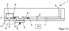
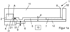
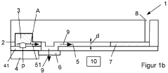
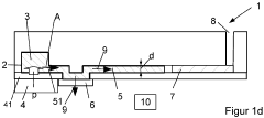
Microfluidic device and method for influencing the flow of a liquid in a microfluidic device
PatentActiveDE102015101106A1
Innovation
- The use of a liquid-impermeable but gas-permeable membrane to cover the microfluidic channel, allowing for controlled fluid flow while permitting gas exchange.
- Incorporation of a liquid-absorbing absorber material downstream of the membrane to influence and control the liquid flow direction and rate.
- The combination of overpressure generation via an actuator with selective membrane permeability to create a sophisticated flow control system in microfluidic devices.
Material Science Considerations for Twisted Interfaces
The interface between two-dimensional materials with a relative twist angle represents a critical frontier in materials science for twistronics applications in microfluidic systems. When layers of 2D materials like graphene or transition metal dichalcogenides are stacked with a slight angular misalignment, they form moiré superlattices that dramatically alter electronic, mechanical, and fluidic properties at the interface.
Material selection for twisted interfaces requires careful consideration of lattice constants, interlayer coupling strength, and chemical stability. Graphene-graphene interfaces have demonstrated remarkable electronic property modulation at the "magic angle" of approximately 1.1°, where superconductivity emerges. However, for microfluidic applications, hexagonal boron nitride (hBN) and molybdenum disulfide (MoS2) interfaces offer superior chemical resistance and controlled hydrophilicity.
Surface engineering of twisted interfaces presents unique challenges in maintaining precise angular alignment during fabrication. Advanced techniques such as dry transfer methods with rotational control have achieved angular precision within 0.1°. The stability of these interfaces under fluid flow conditions depends critically on encapsulation strategies and edge termination methods to prevent delamination or angular drift during operation.
Characterization of twisted interfaces requires specialized approaches beyond conventional materials analysis. Scanning tunneling microscopy can visualize moiré patterns directly, while Raman spectroscopy provides insights into interlayer coupling strength. For microfluidic applications, atomic force microscopy with fluid cells enables in-situ measurement of nanoscale fluid behavior at twisted interfaces.
The mechanical properties of twisted interfaces exhibit fascinating emergent phenomena. Interlayer friction can be tuned by orders of magnitude through precise angle control, creating opportunities for novel fluid flow regulation at the nanoscale. Strain engineering of twisted interfaces further enables dynamic modulation of channel properties during microfluidic operation.
Thermal management considerations are particularly important as twisted interfaces can exhibit significantly altered thermal conductivity compared to aligned layers. Heat dissipation pathways become highly anisotropic, requiring careful thermal design to prevent hotspot formation during operation of microfluidic devices, especially when integrated with electronic components for sensing or actuation purposes.
Defect engineering emerges as both a challenge and opportunity in twisted interface materials. While uncontrolled defects can disrupt the desired moiré pattern, strategically introduced defects can serve as nucleation sites for specific fluid behaviors or as anchoring points to enhance interface stability under flow conditions.
Scalability and Manufacturing Challenges
The scalability of twistronics technology for microfluidic applications faces significant manufacturing challenges that must be addressed before widespread commercial implementation becomes viable. Current fabrication methods for twisted bilayer graphene and other twistronics materials rely heavily on manual processes, particularly in achieving precise twist angles between layers. This manual approach results in low throughput, high variability, and prohibitive costs for large-scale production.
Manufacturing consistency represents a critical barrier, as even minor deviations in twist angles (as small as 0.1 degrees) can dramatically alter the electronic and mechanical properties of the resulting materials. This precision requirement exceeds the capabilities of most conventional semiconductor manufacturing equipment, necessitating the development of specialized tools and processes specifically designed for twistronics fabrication.
Integration challenges further complicate scalability efforts. Incorporating twistronics elements into existing microfluidic platforms requires novel interface solutions that maintain the integrity of both the twisted material structures and the microfluidic channels. Current bonding and integration techniques often compromise the carefully engineered twist angles or damage the delicate layered structures.
Material supply chain limitations also present significant obstacles. High-quality, atomically clean 2D materials required for twistronics applications remain difficult to source at scale. The production of these base materials with consistent quality and at volumes necessary for industrial applications represents an unresolved challenge in the manufacturing ecosystem.
Recent advances in automated assembly systems show promise for addressing some of these challenges. Computer-vision guided robotic systems capable of achieving sub-degree precision in layer alignment have demonstrated improved consistency in laboratory settings. However, these systems still operate at speeds incompatible with high-volume manufacturing requirements.
Economic considerations further complicate the scaling equation. The current cost structure of twistronics fabrication makes it prohibitively expensive for all but the highest-value microfluidic applications. A significant reduction in production costs—likely requiring fundamental innovations in manufacturing methodology—will be necessary before twistronics-enhanced microfluidic systems can penetrate mainstream markets.
Standardization efforts across the industry remain in nascent stages, with various research groups and companies employing different fabrication approaches and quality metrics. This fragmentation impedes the development of unified manufacturing protocols and quality control standards essential for industrial-scale production.
Unlock deeper insights with PatSnap Eureka Quick Research — get a full tech report to explore trends and direct your research. Try now!
Generate Your Research Report Instantly with AI Agent
Supercharge your innovation with PatSnap Eureka AI Agent Platform!