Hybrid Electronic-Photonic Integration For Edge AI Inference
AUG 29, 20259 MIN READ
Generate Your Research Report Instantly with AI Agent
Patsnap Eureka helps you evaluate technical feasibility & market potential.
Hybrid Electronic-Photonic Integration Background and Objectives
Hybrid electronic-photonic integration represents a convergence of electronic and photonic technologies, combining the computational power of electronics with the high-speed data transmission capabilities of photonics. This integration has evolved significantly over the past two decades, transitioning from discrete components to increasingly integrated solutions that leverage the strengths of both domains.
The evolution began with simple optical interconnects in data centers, progressing through silicon photonics platforms that enabled higher integration densities, and now moving toward heterogeneous integration approaches that combine multiple material systems. Recent advancements in manufacturing techniques, particularly in wafer-scale integration and 3D packaging, have accelerated this technological progression, making hybrid solutions increasingly viable for commercial applications.
Current technology trends point toward greater functional integration, with photonic neural networks emerging as a promising approach for accelerating specific computational workloads. The miniaturization of photonic components and improvements in coupling efficiency between electronic and photonic domains represent critical evolutionary paths that continue to drive innovation in this field.
The primary objective of hybrid electronic-photonic integration for edge AI inference is to overcome the fundamental limitations of traditional electronic systems in terms of power consumption, latency, and bandwidth when processing complex AI workloads at the network edge. By leveraging photonics for specific computational tasks and data movement while maintaining electronic control and memory functions, these hybrid systems aim to deliver orders-of-magnitude improvements in energy efficiency and processing speed.
Additional technical objectives include developing architectures that can effectively partition workloads between electronic and photonic domains, creating efficient interfaces between these domains with minimal conversion losses, and designing systems that can be manufactured at scale using processes compatible with existing semiconductor fabrication infrastructure.
From a practical perspective, the technology aims to enable real-time AI inference capabilities in edge devices with strict power and form factor constraints, such as autonomous vehicles, smart sensors, and mobile devices. This would allow complex neural network models to be executed locally without requiring cloud connectivity, thereby improving privacy, reducing latency, and enabling operation in connectivity-limited environments.
The long-term vision for this technology extends beyond simple acceleration to fundamentally new computing paradigms that leverage the unique properties of light for computation, potentially enabling entirely new classes of AI algorithms and applications that would be impractical with purely electronic implementations.
Market Demand Analysis for Edge AI Inference Solutions
The edge AI inference market is experiencing unprecedented growth, driven by the increasing demand for real-time processing capabilities in various applications. Current market analysis indicates that the global edge AI hardware market is projected to reach $38 billion by 2026, with a compound annual growth rate of approximately 20.3%. This rapid expansion is primarily fueled by the need to process massive amounts of data locally, reducing latency and bandwidth requirements while enhancing privacy and security.
The integration of hybrid electronic-photonic systems for edge AI inference is responding to critical market demands across multiple sectors. In telecommunications, the need for high-speed, energy-efficient data processing at network edges is becoming paramount as 5G and future 6G networks expand. Telecommunications providers are actively seeking solutions that can handle the exponential growth in data traffic without corresponding increases in power consumption.
In the automotive industry, advanced driver-assistance systems (ADAS) and autonomous vehicles require instantaneous processing of sensor data, creating a substantial market for edge AI solutions that can deliver real-time inference with minimal latency. The market size for AI hardware in automotive applications is expected to grow at 25% annually through 2025.
Healthcare represents another significant market opportunity, with applications ranging from wearable health monitors to point-of-care diagnostic tools. These applications demand not only computational efficiency but also form factor considerations that hybrid electronic-photonic solutions are uniquely positioned to address.
Industrial IoT applications constitute a rapidly expanding market segment, with manufacturing facilities deploying increasing numbers of sensors and edge devices. The industrial edge computing market is growing at 19.8% annually, with AI inference capabilities being a key component of this growth.
Consumer electronics manufacturers are also driving demand for more efficient edge AI solutions as they integrate increasingly sophisticated AI capabilities into smartphones, smart home devices, and wearables. These applications are particularly sensitive to power consumption constraints, making energy-efficient hybrid solutions especially valuable.
Market research indicates that customers across these sectors share common requirements: reduced power consumption (with targets of 10-100x improvement over current solutions), decreased latency (sub-millisecond response times), increased computational density, and improved reliability. Hybrid electronic-photonic integration addresses these needs by leveraging the complementary strengths of electronic and photonic technologies.
The market is also showing strong preference for scalable solutions that can adapt to varying computational demands and deployment scenarios, from resource-constrained IoT devices to more capable edge servers. This versatility requirement aligns well with the modular nature of hybrid integration approaches.
Current State and Challenges in Hybrid Integration Technologies
Hybrid electronic-photonic integration technology currently stands at a critical juncture, with significant advancements achieved in recent years but still facing substantial challenges for widespread edge AI deployment. The current state of this technology is characterized by a growing ecosystem of research institutions and commercial entities working on various integration approaches, with monolithic, heterogeneous, and 3D integration being the primary methodologies.
Monolithic integration has demonstrated promising results in research settings, particularly with silicon photonics platforms that integrate electronic and photonic components on the same substrate. However, commercial-scale manufacturing remains limited due to material compatibility issues between electronic CMOS processes and photonic fabrication requirements.
Heterogeneous integration, which combines separately fabricated electronic and photonic chips, has gained traction as a more practical near-term solution. Companies like Intel, IBM, and Ayar Labs have made significant progress in this domain, with Ayar Labs' optical I/O solution representing one of the most advanced commercial implementations to date.
The performance metrics of current hybrid systems show impressive improvements in energy efficiency, with demonstrations achieving 1-2 orders of magnitude better performance per watt compared to traditional electronic systems for specific AI workloads. Latency reductions of 30-50% have been reported in laboratory settings, particularly for matrix multiplication operations central to neural network inference.
Despite these advances, several critical challenges persist. Manufacturing scalability remains perhaps the most significant hurdle, with current fabrication processes lacking the maturity and yield rates necessary for high-volume production. The integration density achievable today falls short of what's required for complex edge AI models, limiting the practical applications.
Thermal management presents another major challenge, as photonic components often have strict temperature stability requirements that conflict with the heat generated by electronic processors. Current cooling solutions add significant bulk and power requirements, undermining the size and efficiency advantages sought in edge devices.
Standardization across the industry remains fragmented, with competing approaches to interfaces, packaging, and testing methodologies. This lack of standardization increases development costs and slows market adoption, as system designers must navigate proprietary solutions with limited interoperability.
The talent gap represents another significant constraint, with relatively few engineers possessing expertise in both electronic and photonic domains. Educational institutions are only beginning to develop integrated curricula addressing this emerging field, creating a bottleneck in workforce development that limits innovation pace.
Current Technical Solutions for Edge AI Inference
01 Integration of electronic and photonic components on a single platform
Hybrid electronic-photonic integration involves combining electronic and photonic components on a single platform to leverage the advantages of both technologies. This integration enables high-speed data processing and transmission while reducing power consumption and form factor. The integration can be achieved through various fabrication techniques, including monolithic integration, heterogeneous integration, or 3D stacking, allowing for improved system performance and functionality.- Integration of electronic and photonic components on a single platform: Hybrid electronic-photonic integration involves combining electronic and photonic components on a single platform to leverage the advantages of both technologies. This integration enables high-speed data processing and transmission while reducing power consumption and size. The integration can be achieved through various fabrication techniques, including monolithic integration, heterogeneous integration, and 3D stacking, allowing for compact and efficient systems with enhanced performance.
- Performance optimization through novel materials and structures: The performance of hybrid electronic-photonic integrated circuits can be significantly enhanced through the use of novel materials and structures. These include silicon-based photonics, III-V semiconductors, and 2D materials that offer improved light emission, detection, and modulation capabilities. Advanced waveguide structures, resonators, and gratings are employed to optimize light propagation and coupling between electronic and photonic components, resulting in higher bandwidth, lower latency, and improved signal integrity.
- Signal processing and communication enhancements: Hybrid electronic-photonic integration enables advanced signal processing and communication capabilities. These systems incorporate high-speed modulators, photodetectors, and optical amplifiers alongside electronic control circuits to achieve efficient signal conversion between electronic and optical domains. Various modulation schemes, wavelength division multiplexing, and optical switching techniques are implemented to increase data throughput and reduce latency in communication networks, data centers, and high-performance computing applications.
- Thermal management and energy efficiency: Effective thermal management is crucial for maintaining the performance of hybrid electronic-photonic integrated circuits. Various cooling techniques and thermal isolation structures are employed to mitigate heat-related issues that can affect both electronic and photonic components. Energy-efficient designs incorporate low-power electronic drivers, optimized optical paths, and intelligent power management systems to reduce overall power consumption while maintaining high performance, making these systems suitable for applications with strict power constraints.
- Packaging and interconnect solutions: Advanced packaging and interconnect technologies are essential for realizing the full potential of hybrid electronic-photonic integrated systems. These include fiber-to-chip coupling techniques, through-silicon vias, interposers, and flip-chip bonding that enable efficient connections between electronic and photonic components. Novel packaging approaches address challenges related to alignment precision, mechanical stability, and environmental protection, ensuring reliable operation across various conditions while facilitating integration with existing electronic systems.
02 Performance enhancement through novel materials and structures
The performance of hybrid electronic-photonic integrated circuits can be significantly enhanced through the use of novel materials and structures. These include silicon-based photonics, III-V semiconductors, graphene, and other 2D materials that offer improved optical and electronic properties. Advanced structures such as photonic crystals, ring resonators, and waveguides can be engineered to optimize light propagation, modulation, and detection, resulting in higher bandwidth, lower latency, and improved signal integrity.Expand Specific Solutions03 Signal conversion and processing techniques
Efficient conversion between electronic and optical signals is crucial for hybrid integration performance. Advanced modulation schemes, signal processing algorithms, and conversion techniques are employed to minimize conversion losses and maximize bandwidth. These techniques include electro-optic modulation, direct modulation of lasers, coherent detection, and digital signal processing, which collectively enhance the overall system performance by enabling higher data rates, improved signal quality, and reduced power consumption.Expand Specific Solutions04 Thermal management and energy efficiency
Thermal management is a critical aspect of hybrid electronic-photonic integration as it affects both the performance and reliability of integrated devices. Various cooling strategies, heat dissipation techniques, and thermally-aware designs are implemented to maintain optimal operating temperatures. Additionally, energy-efficient architectures and low-power operation modes are developed to reduce power consumption while maintaining high performance, making these integrated systems suitable for a wide range of applications from data centers to mobile devices.Expand Specific Solutions05 Packaging and interconnect solutions
Advanced packaging and interconnect solutions are essential for maximizing the performance of hybrid electronic-photonic integrated systems. These include through-silicon vias (TSVs), optical interposers, 3D packaging, and chip-to-chip optical interconnects that enable high-bandwidth, low-latency communication between components. Novel coupling techniques between optical fibers and on-chip waveguides, as well as between different photonic and electronic layers, help minimize insertion losses and improve overall system efficiency and reliability.Expand Specific Solutions
Key Industry Players in Hybrid Integration for AI
The hybrid electronic-photonic integration for edge AI inference market is currently in an early growth phase, characterized by increasing research activities and emerging commercial applications. The market size is expanding rapidly, driven by demand for energy-efficient AI processing at the edge, with projections suggesting significant growth over the next five years. From a technical maturity perspective, the field remains developing but advancing quickly, with key players demonstrating varying levels of expertise. Industry leaders include GlobalFoundries and Huawei, who leverage their semiconductor manufacturing capabilities, while specialized photonics companies like Skorpios Technologies and Anello Photonics focus on innovative integration approaches. Academic institutions such as MIT, Shanghai Jiao Tong University, and Beijing Institute of Technology are contributing fundamental research, while HP Development and Hewlett Packard Enterprise are exploring commercial applications for data centers and edge computing.
Huawei Technologies Co., Ltd.
Technical Solution: Huawei has developed a comprehensive hybrid electronic-photonic integration platform for edge AI inference called "Ascend-Photonics." This solution combines their Ascend AI processors with integrated silicon photonics to accelerate neural network operations. Huawei's approach utilizes photonic integrated circuits (PICs) for high-speed data transmission between processing nodes while leveraging electronic components for control logic and memory access. Their architecture implements optical matrix multiplication units that can process multiple AI inference operations in parallel using wavelength multiplexing techniques. Huawei has demonstrated energy efficiency improvements of up to 20x compared to electronic-only solutions for specific AI workloads. The platform incorporates proprietary optical interconnect technology that enables chip-to-chip communication at speeds exceeding 100 Gbps per channel while consuming minimal power. Huawei has optimized their solution specifically for edge deployment scenarios with constrained power budgets, such as telecommunications infrastructure and smart city applications.
Strengths: Highly optimized for telecommunications infrastructure, excellent power efficiency for distributed edge computing scenarios, and mature manufacturing capabilities for volume production. Weaknesses: Proprietary ecosystem may limit broader adoption, and the solution requires specialized software frameworks to fully utilize the hybrid architecture, creating potential integration challenges with existing AI workflows.
Massachusetts Institute of Technology
Technical Solution: MIT has pioneered hybrid electronic-photonic integration for edge AI inference through their development of advanced photonic neural network architectures. Their approach combines silicon photonics with CMOS electronics to create energy-efficient AI accelerators. MIT's technology utilizes wavelength division multiplexing (WDM) to perform parallel matrix operations optically, while maintaining electronic control for programming flexibility. Their integrated photonic tensor cores can process multiple AI operations simultaneously at the speed of light, achieving computational densities exceeding 100 TOPS/W. MIT researchers have demonstrated photonic neural networks that can perform inference tasks with significantly reduced latency (sub-nanosecond) compared to electronic-only solutions. Their platform incorporates on-chip optical memory elements and programmable photonic meshes that enable reconfigurable neural network implementations suitable for edge deployment.
Strengths: Exceptional energy efficiency (100+ TOPS/W), ultra-low latency processing, and high bandwidth density. MIT's solution excels in applications requiring real-time processing of high-dimensional data. Weaknesses: Requires precise temperature control systems, increasing system complexity, and faces challenges in scaling manufacturing to commercial volumes due to integration complexities between electronic and photonic components.
Core Innovations in Electronic-Photonic Integration
Optical modulator driver for photonic interconnect platforms
PatentWO2025145108A1
Innovation
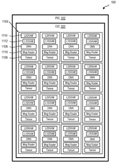
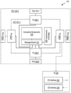
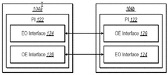
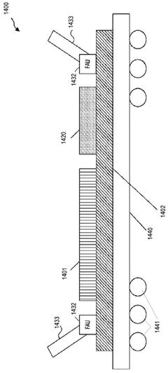
- A photonic interconnect platform featuring hybrid electro-photonic integrated circuit packages with electro-absorption modulators (EAMs) positioned close to active electronic elements, utilizing optical modulator drivers and transimpedance amplifiers to enable efficient data routing through optical and electrical channels, reducing noise and power consumption.
Artificial intelligence inference architecture with hardware acceleration
PatentPendingUS20220358370A1
Innovation
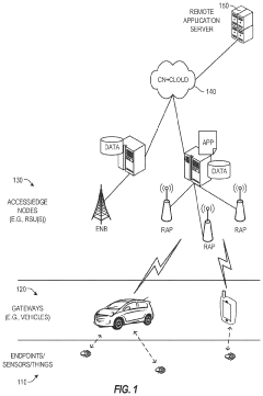
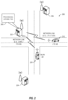
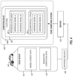
- The implementation of a headless aggregation AI configuration that enables seamless access to AI inferencing capabilities on edge computing hardware through an AI model description, utilizing specialized hardware platforms like FPGAs and neural network accelerators, with logic for AI model generation, request scheduling, and processing, reducing the need for software intervention and optimizing resource usage.
Energy Efficiency Considerations for Edge Deployment
Energy efficiency stands as a critical factor in the deployment of hybrid electronic-photonic systems for edge AI inference. Traditional electronic computing architectures face significant power constraints when executing complex AI workloads at the edge, with thermal dissipation and battery life presenting substantial challenges. Hybrid electronic-photonic integration offers promising solutions to these energy efficiency bottlenecks through several key mechanisms.
The fundamental energy advantage of photonic computing stems from the near-zero heat generation during photon propagation and manipulation, contrasting sharply with electron-based computation which generates substantial heat through resistance. Measurements indicate that photonic neural network accelerators can achieve energy efficiencies below 1 picojoule per multiply-accumulate operation (MAC), representing orders of magnitude improvement over electronic counterparts that typically consume 10-100 picojoules per MAC.
When deployed at the edge, hybrid systems must optimize the energy distribution between electronic control components and photonic processing elements. Current implementations demonstrate that the electronic-photonic interface often constitutes a significant energy overhead, consuming 30-40% of the total system power. Advances in efficient electro-optic modulators and photodetectors are progressively reducing this conversion penalty.
Operational wavelength selection significantly impacts energy efficiency, with silicon photonics platforms operating at 1550nm showing superior energy performance compared to visible light implementations. Recent research demonstrates that wavelength division multiplexing (WDM) techniques can further enhance computational density without proportional energy increases, enabling parallel processing capabilities that are particularly valuable for convolutional neural network operations.
Dynamic power management represents another crucial consideration for edge deployment. Unlike purely electronic systems, photonic components offer unique opportunities for selective activation based on computational demands. Emerging architectures implement power-gating techniques for optical modulators and detectors, allowing portions of the photonic circuitry to remain dormant during periods of reduced computational load.
Thermal management strategies must also be reconsidered for hybrid systems. While photonic components generate less heat during operation, they often exhibit greater temperature sensitivity. Edge deployments therefore require careful thermal isolation between electronic and photonic subsystems, with some implementations incorporating microfluidic cooling channels specifically designed for the photonic layers to maintain operational stability across varying environmental conditions.
Scalability and Manufacturing Challenges
The scalability of hybrid electronic-photonic integration for edge AI inference faces significant manufacturing challenges that must be addressed to enable widespread adoption. Current fabrication processes for integrated photonic components often require specialized equipment and clean room facilities, making mass production costly and complex. The integration of electronic and photonic components on the same substrate introduces thermal management issues, as photonic elements are typically more sensitive to temperature variations than their electronic counterparts.
Material compatibility presents another major hurdle. Silicon photonics has emerged as a promising platform due to its compatibility with CMOS processes, but the integration of III-V materials for light sources remains challenging. Heterogeneous integration techniques such as wafer bonding and flip-chip assembly have shown promise but still face yield and reliability issues at scale.
Dimensional precision requirements further complicate manufacturing. Photonic waveguides require nanometer-scale precision, significantly exceeding the tolerances typical in electronic circuit fabrication. This necessitates advanced lithography techniques and precise process control, increasing production costs and potentially limiting yield rates.
Testing and quality assurance represent additional scalability challenges. Unlike electronic circuits, which can be tested using established electrical probing methods, photonic components require specialized optical testing equipment and procedures. The development of standardized testing protocols for hybrid systems remains in its early stages, complicating quality control in mass production scenarios.
Supply chain considerations also impact scalability. The photonic component ecosystem is less mature than its electronic counterpart, with fewer suppliers and less standardization. This creates potential bottlenecks in sourcing specialized materials and components required for hybrid integration.
Cost-effective packaging solutions present perhaps the most significant barrier to widespread adoption. Fiber-to-chip coupling remains labor-intensive and difficult to automate, while hermetic sealing requirements for photonic components add complexity. Current packaging costs can represent up to 80% of the total device cost, making economical scaling challenging.
Addressing these manufacturing challenges requires collaborative efforts between electronic and photonic industries to develop standardized processes, design rules, and testing methodologies. Recent advances in silicon photonics foundry services and photonic design automation tools show promise, but significant investment in manufacturing infrastructure and process development remains necessary to achieve the scalability required for mainstream edge AI applications.
Unlock deeper insights with Patsnap Eureka Quick Research — get a full tech report to explore trends and direct your research. Try now!
Generate Your Research Report Instantly with AI Agent
Supercharge your innovation with Patsnap Eureka AI Agent Platform!
