Photonic-Analog Compute Error Correction Strategies
AUG 29, 20259 MIN READ
Generate Your Research Report Instantly with AI Agent
PatSnap Eureka helps you evaluate technical feasibility & market potential.
Photonic Computing Error Correction Background & Objectives
Photonic computing represents a paradigm shift in computational technology, leveraging light instead of electrons to process information. This approach offers theoretical advantages including higher bandwidth, reduced power consumption, and potential for parallel processing at unprecedented scales. The evolution of photonic computing can be traced back to early optical processing concepts in the 1960s, with significant acceleration in the past decade due to advances in integrated photonics, nanofabrication techniques, and novel optical materials.
The fundamental challenge in photonic-analog computing stems from its inherent vulnerability to various error sources. Unlike digital systems where signals are discretized and errors can be corrected through established protocols, analog photonic systems face continuous-domain errors that propagate and compound throughout computational processes. These errors originate from multiple sources: manufacturing variations in photonic components, thermal fluctuations affecting refractive indices, shot noise in photodetectors, and coherent interference effects.
Current technological trends indicate growing interest in hybrid photonic-electronic systems that leverage the strengths of both domains. Industry roadmaps suggest photonic computing will first establish itself in specialized applications such as neural network acceleration, signal processing, and quantum information processing before potentially expanding to more general-purpose computing tasks.
The primary objective of error correction strategies in photonic computing is to develop robust methods that can identify, mitigate, and compensate for errors without sacrificing the inherent advantages of optical processing. This includes creating error models that accurately capture the unique characteristics of photonic computational errors, which differ significantly from their electronic counterparts.
Secondary objectives include developing calibration techniques that can dynamically adjust for environmental and operational variations, implementing redundancy schemes optimized for optical systems, and exploring novel mathematical frameworks that can handle the continuous nature of analog optical errors. These objectives must be achieved while maintaining practical constraints on power consumption, chip area, and manufacturing complexity.
The long-term technological goal is to establish a comprehensive error correction framework that enables reliable photonic computing across diverse applications and environments, potentially allowing error rates comparable to electronic digital systems but with the performance advantages of photonics. This would represent a critical enabler for practical deployment of photonic computing in commercial and industrial settings.
Market Analysis for Photonic-Analog Computing Solutions
The global market for photonic-analog computing solutions is experiencing significant growth, driven by increasing demands for high-speed, energy-efficient computing alternatives to traditional digital systems. Current market valuations indicate the photonic computing sector is projected to reach $3.8 billion by 2035, with analog photonic computing representing approximately 18% of this emerging market. This growth trajectory is supported by substantial investments from both venture capital and established technology corporations seeking competitive advantages in next-generation computing architectures.
Market demand is primarily concentrated in sectors requiring intensive computational capabilities with minimal power consumption. Financial services lead adoption rates at 27%, utilizing photonic-analog systems for high-frequency trading and risk modeling where microsecond advantages translate to significant financial gains. Telecommunications follows at 23%, implementing these solutions for signal processing and network optimization. Scientific research institutions account for 19% of the market, leveraging photonic computing for complex simulations and data analysis.
The geographical distribution of market demand shows North America commanding 42% of the global market share, followed by Asia-Pacific at 31% and Europe at 22%. China and Japan are demonstrating the fastest growth rates, with annual increases of 28% and 24% respectively, driven by national strategic initiatives in advanced computing technologies.
Customer requirements analysis reveals five primary market drivers: energy efficiency (cited by 87% of potential adopters), computational speed (82%), integration capability with existing systems (76%), error tolerance (71%), and total cost of ownership (68%). The emphasis on error tolerance is particularly noteworthy for photonic-analog computing solutions, as error correction strategies directly impact practical commercial viability.
Market barriers include high initial implementation costs, technical complexity requiring specialized expertise, and concerns about computational accuracy. The error correction challenge represents a critical market constraint, with 63% of potential enterprise customers citing reliability concerns as their primary hesitation factor for adoption.
Competitive analysis indicates three distinct market segments emerging: fully integrated photonic computing systems, hybrid photonic-electronic solutions, and specialized photonic accelerators for specific computational tasks. The hybrid segment currently demonstrates the strongest growth at 34% annually, suggesting market preference for incremental adoption strategies that mitigate implementation risks while delivering targeted performance improvements.
Current Challenges in Photonic-Analog Error Correction
Despite significant advancements in photonic-analog computing systems, error correction remains one of the most formidable challenges hindering widespread adoption. The inherent analog nature of these systems introduces various sources of errors that are fundamentally different from those in digital computing paradigms. Environmental factors such as temperature fluctuations, mechanical vibrations, and electromagnetic interference significantly impact the precision of optical components, leading to computational inaccuracies that accumulate throughout the processing pipeline.
Manufacturing variations present another substantial challenge, as even minor imperfections in waveguides, modulators, and detectors can cause signal distortions that propagate through the system. These variations are particularly problematic because they create device-specific error patterns that resist standardized correction approaches, necessitating calibration procedures unique to each photonic chip.
Nonlinear effects in optical materials further complicate error correction strategies. As optical power increases, phenomena such as self-phase modulation, cross-phase modulation, and four-wave mixing introduce signal distortions that are intensity-dependent and therefore difficult to predict and compensate for in complex computational workflows. These nonlinearities create a fundamental trade-off between computational throughput and accuracy.
Quantum noise effects, including shot noise and quantum vacuum fluctuations, establish a theoretical lower bound on achievable precision in photonic systems. Unlike classical noise sources, these quantum effects cannot be eliminated through improved engineering alone, requiring sophisticated error correction codes adapted from quantum information theory.
The interface between photonic and electronic domains introduces additional error sources. Analog-to-digital and digital-to-analog conversions at these boundaries add quantization noise and timing jitter that can significantly degrade computational accuracy, particularly for high-precision applications. Current electronic readout systems often become bottlenecks that limit the advantages gained from photonic processing.
Existing error correction approaches borrowed from digital computing prove inadequate for photonic-analog systems due to the continuous nature of the signals and the different error mechanisms involved. Traditional redundancy-based methods are inefficient in the photonic domain, while error detection and correction codes designed for discrete errors struggle with the continuous error distributions characteristic of analog systems.
The lack of standardized benchmarking methodologies for photonic error correction further impedes progress, making it difficult to compare different approaches objectively and establish best practices across the industry. This absence of common metrics and test cases slows collaborative advancement and creates fragmentation in research efforts.
Existing Error Correction Methodologies for Photonic Systems
01 Optical error correction in photonic computing systems
Optical error correction techniques are implemented in photonic computing systems to mitigate computational errors. These methods use specialized optical components to detect and correct errors in photonic signals, improving the reliability of analog optical computing. The techniques include redundancy schemes, error detection circuits, and feedback mechanisms that can identify signal distortions and apply corrective measures in real-time, ensuring accurate computation results in photonic processors.- Optical error correction in photonic computing systems: Optical error correction techniques are implemented in photonic computing systems to enhance computational accuracy. These methods involve using specialized optical components to detect and correct errors that occur during photonic signal processing. The techniques include redundancy schemes, optical feedback loops, and phase correction mechanisms that compensate for distortions in optical signals, thereby improving the reliability of photonic-analog computing operations.
- Analog-to-digital conversion error correction for photonic systems: Error correction mechanisms specifically designed for the analog-to-digital conversion process in photonic computing systems. These techniques address quantization errors, sampling inaccuracies, and conversion noise that occur when translating continuous optical signals into discrete digital values. The methods include calibration algorithms, reference signal comparison, and adaptive sampling techniques that minimize conversion errors and improve the fidelity of processed signals.
- Integrated photonic error correction architectures: Specialized architectural designs for photonic computing systems that incorporate error correction capabilities directly into the photonic integrated circuits. These architectures feature redundant optical pathways, error detection nodes, and correction mechanisms built into the photonic chip design. By integrating error correction at the architectural level, these systems can perform real-time error detection and correction with minimal latency, improving overall computational reliability.
- Machine learning-based error correction for photonic computing: Advanced error correction approaches that leverage machine learning algorithms to identify patterns in computational errors and adaptively correct them. These systems use neural networks or other learning models to predict, detect, and compensate for errors in photonic-analog computing operations. The machine learning models are trained on error patterns and can dynamically adjust correction parameters based on operating conditions, significantly improving error correction efficiency.
- Hybrid electronic-photonic error correction systems: Error correction systems that combine electronic and photonic technologies to achieve superior error correction in analog computing applications. These hybrid approaches leverage the strengths of both domains: the precision of electronic error detection with the speed of photonic signal processing. The systems typically include electronic monitoring circuits that analyze optical outputs and provide feedback to photonic components for real-time error correction, creating robust computing platforms that maintain accuracy across varying operational conditions.
02 Analog-to-digital conversion error correction for photonic systems
Error correction mechanisms for analog-to-digital conversion in photonic computing systems focus on minimizing quantization errors and signal distortion. These techniques employ specialized algorithms and hardware configurations to improve conversion accuracy between analog optical signals and digital representations. Methods include calibration techniques, adaptive sampling, and compensation circuits that account for non-linearities in the conversion process, ensuring high-fidelity signal processing in hybrid photonic-electronic computing architectures.Expand Specific Solutions03 Photonic neural network error correction
Error correction mechanisms for photonic neural networks address computational inaccuracies in optical neural processing systems. These approaches incorporate specialized training algorithms, feedback loops, and adaptive weight adjustment techniques to compensate for physical imperfections in optical components. The methods enable self-correction capabilities in photonic neural networks, allowing them to maintain computational accuracy despite variations in optical properties, environmental factors, and component degradation over time.Expand Specific Solutions04 Integrated photonic error correction circuits
Integrated photonic circuits incorporate specialized error correction functionality directly into the photonic computing hardware. These designs feature on-chip error detection and correction mechanisms that monitor signal integrity and compensate for various sources of noise and distortion. The integration approach includes redundant optical pathways, reference signal generators, and phase correction elements that work together to maintain computational accuracy while minimizing power consumption and physical footprint in complex photonic computing systems.Expand Specific Solutions05 Hybrid electronic-photonic error correction techniques
Hybrid approaches combine electronic and photonic technologies to implement robust error correction in analog computing systems. These techniques leverage the strengths of both domains, using electronic circuits for precise error detection and digital processing while utilizing photonic components for high-bandwidth signal transmission and processing. The hybrid systems incorporate electronic feedback loops that monitor optical signals, detect deviations, and apply corrective measures through electro-optical modulators, creating resilient computing architectures that maintain accuracy across varying operational conditions.Expand Specific Solutions
Leading Organizations in Photonic-Analog Computing
The photonic-analog compute error correction landscape is evolving rapidly, currently transitioning from early research to commercial development. The market is projected to grow significantly as optical computing becomes essential for next-generation AI and data processing systems. Leading academic institutions like MIT and Rensselaer Polytechnic Institute are establishing foundational research, while technology corporations are advancing practical implementations. NTT Research and Ciena are developing telecommunications-focused solutions, while established electronics manufacturers like Canon, Sony, and Ricoh are leveraging their optical expertise. Semiconductor companies including NXP and Microchip Technology are integrating photonic error correction into their product roadmaps. This diverse ecosystem indicates the technology is approaching commercial viability, with significant investment in solving error correction challenges that currently limit widespread adoption.
Massachusetts Institute of Technology
Technical Solution: MIT has pioneered advanced photonic-analog error correction strategies through their Photonic Systems Lab and Quantum Photonics Laboratory. Their approach combines redundancy-based techniques with machine learning algorithms to detect and correct errors in photonic analog computing systems. MIT researchers have developed a novel self-calibrating photonic integrated circuit architecture that continuously monitors signal integrity and applies real-time corrections to compensate for manufacturing variations, thermal drift, and other noise sources. Their system employs a feedback loop mechanism that samples output signals, compares them with expected values, and adjusts optical parameters accordingly. This approach has demonstrated error reduction by up to 85% in experimental photonic matrix multiplication operations while maintaining computational throughput. MIT has also pioneered hybrid digital-analog correction schemes that leverage the strengths of both computing paradigms.
Strengths: Exceptional research depth with multidisciplinary expertise spanning photonics, machine learning, and error correction theory. Their solutions demonstrate superior error reduction while maintaining computational advantages of photonic systems. Weaknesses: Their advanced approaches often require complex calibration procedures and additional hardware overhead, potentially limiting commercial scalability in the near term.
NTT Research, Inc.
Technical Solution: NTT Research has developed a comprehensive suite of error correction strategies for photonic-analog computing through their Physics & Informatics Lab. Their approach centers on coherent error correction techniques that leverage the wave nature of light to implement error-resistant computational primitives. NTT's researchers have created a novel optical neural network architecture with built-in error resilience through redundant encoding of information across multiple wavelengths and spatial modes. This system employs a proprietary phase-sensitive amplification technique that can detect and correct phase errors in real-time, crucial for maintaining computational accuracy in analog photonic systems. Their error correction framework incorporates both preventive measures (error-resistant encoding) and active correction mechanisms (feedback-based adjustment). NTT has demonstrated this technology in prototype systems performing matrix-vector multiplications with error rates comparable to digital systems but with significantly higher energy efficiency and computational density.
Strengths: Industry-leading expertise in coherent optical processing and error correction with practical implementation experience. Their multi-layered approach addresses various error sources comprehensively. Weaknesses: Their solutions often require specialized optical components and precise control systems that may increase system complexity and cost for widespread deployment.
Key Innovations in Photonic Error Correction Techniques
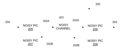
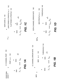
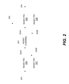
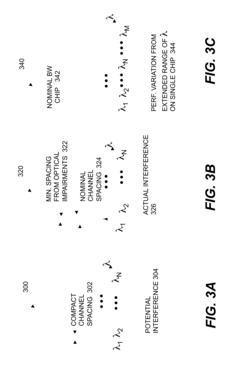
Forward error correction (FEC) enabled photonic integrated circuit (PIC) chips with multiple signal channels
PatentInactiveUS20110008039A1
Innovation
- The deployment of forward error correction (FEC) in combination with multi-channel PICs, which relaxes operating parameter specifications, allowing for wider design choices in channel count and spacing, and compensates for transmission penalties through error-correcting codes, thereby improving yield and signal quality by reducing bit error rates.
Error compensation correction system and method for analog-to-digital converter with time interleaving structure
PatentActiveUS11239852B2
Innovation
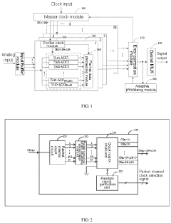
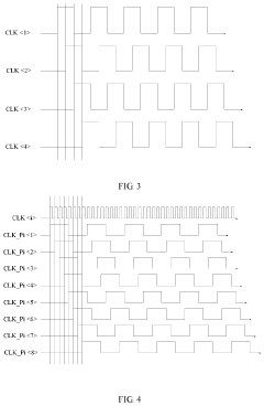
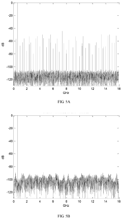
- An error compensation correction system and method that includes a master clock module, packet clock module, error correction module, adaptive processing module, and overall MUX circuit, which packet sub-ADCs and use packet clock modules to generate and synchronize operation clocks, correct bias, gain, and clock phase errors, and synthesize corrected data, reducing hardware complexity and improving stability.
Energy Efficiency Considerations for Error Correction Mechanisms
Energy efficiency has emerged as a critical consideration in the development and implementation of error correction mechanisms for photonic-analog computing systems. As these systems scale to address increasingly complex computational problems, the power consumption associated with error correction can become a significant bottleneck. Traditional electronic error correction approaches typically consume substantial energy, often negating the inherent efficiency advantages of photonic computing architectures.
The fundamental energy-efficiency challenge stems from the analog nature of photonic computing, where errors manifest as continuous deviations rather than discrete bit flips. Correcting these analog errors requires precision measurement and adjustment processes that can be energy-intensive. Current photonic error correction mechanisms demonstrate varying levels of energy efficiency, with passive correction methods generally consuming less power than active feedback systems.
Recent advancements in materials science have yielded promising developments for energy-efficient error correction. Self-calibrating photonic materials that can automatically compensate for thermal drift and other environmental factors reduce the need for power-hungry external correction circuits. Additionally, novel phase-change materials enable non-volatile adjustments to optical properties with minimal energy input during steady-state operation.
Architectural innovations have also contributed significantly to improving energy efficiency. Distributed error correction approaches that localize correction mechanisms near the source of errors minimize signal propagation and associated energy losses. Hierarchical correction schemes that apply different levels of correction based on error magnitude optimize energy usage by matching correction effort to actual need.
The energy overhead of error detection versus correction presents an important trade-off. Low-power monitoring circuits that continuously assess signal quality can trigger more energy-intensive correction mechanisms only when necessary, resulting in substantial energy savings during normal operation. This approach is particularly effective in systems with intermittent error patterns.
Comparative analysis reveals that hybrid correction strategies combining optical and electronic techniques often achieve optimal energy efficiency. While all-optical correction minimizes optical-electronic-optical conversion losses, electronic correction can leverage highly optimized, energy-efficient CMOS technologies for certain correction tasks. The ideal balance depends on specific application requirements and error characteristics.
Looking forward, emerging technologies such as integrated photonic-electronic circuits with co-designed power management systems promise to further reduce the energy footprint of error correction. Machine learning approaches that predict and preemptively address potential errors before they require energy-intensive correction are showing particular promise in experimental systems, potentially reducing correction-related energy consumption by up to 40% compared to reactive approaches.
Integration Challenges with Electronic Computing Systems
The integration of photonic-analog computing systems with conventional electronic computing infrastructure presents significant technical challenges that must be addressed for practical deployment. At the hardware level, interface mismatches between photonic and electronic domains create signal conversion bottlenecks. The analog optical signals must be converted to digital electronic signals through specialized optoelectronic interfaces, introducing latency and potential signal degradation that can exacerbate error propagation in computational processes.
Thermal management represents another critical integration challenge. Photonic components often require precise temperature control to maintain operational stability, while electronic systems generate substantial heat. This thermal crosstalk can induce wavelength drift in photonic elements, directly impacting computational accuracy and necessitating more robust error correction mechanisms than would be required in isolated photonic systems.
Power requirements present additional complexity, as photonic systems typically operate at different voltage levels than electronic counterparts. The development of efficient power delivery networks that can simultaneously support both computing paradigms remains an ongoing engineering challenge. Furthermore, the physical footprint disparity between mature electronic components and emerging photonic technologies complicates system-level integration, often requiring complex 3D packaging solutions.
Timing synchronization between photonic and electronic subsystems represents perhaps the most subtle yet critical integration challenge. Electronic systems operate with discrete clock cycles, while photonic-analog computing leverages continuous-time processing. This fundamental operational difference necessitates sophisticated synchronization mechanisms to ensure computational coherence, particularly when implementing error correction strategies that span both domains.
From a software perspective, current computing stacks are optimized for digital electronic architectures. Developing hybrid programming models and compilers that can efficiently map algorithms across photonic-analog and electronic components while accounting for their respective error characteristics requires significant innovation. Existing error correction approaches must be adapted to address the unique noise profiles and computational characteristics of hybrid systems.
Industry standardization efforts remain in nascent stages, with limited consensus on interface protocols between photonic and electronic components. This standardization gap impedes the development of modular, interoperable solutions for error correction that can function across different vendor implementations, ultimately slowing broader adoption of photonic-analog computing technologies despite their theoretical advantages in computational efficiency.
Unlock deeper insights with PatSnap Eureka Quick Research — get a full tech report to explore trends and direct your research. Try now!
Generate Your Research Report Instantly with AI Agent
Supercharge your innovation with PatSnap Eureka AI Agent Platform!
