Scaling Photonic Interconnects For Multi-Chip Neuromorphic Systems
AUG 29, 20259 MIN READ
Generate Your Research Report Instantly with AI Agent
Patsnap Eureka helps you evaluate technical feasibility & market potential.
Photonic Interconnect Evolution and Objectives
Photonic interconnect technology has evolved significantly over the past three decades, transitioning from simple optical links to sophisticated integrated photonic networks. The initial development phase in the 1990s focused primarily on point-to-point optical connections using vertical-cavity surface-emitting lasers (VCSELs) and multimode fibers, which offered modest bandwidth improvements over electrical interconnects. By the early 2000s, wavelength division multiplexing (WDM) techniques began to emerge in datacenter applications, enabling multiple data channels on a single physical link.
The mid-2010s marked a pivotal shift with the introduction of silicon photonics platforms that facilitated the integration of optical components directly with CMOS electronics. This integration dramatically reduced the size, power consumption, and cost of photonic interconnects while simultaneously increasing bandwidth density. Recent advancements have pushed data rates from 25 Gbps to beyond 100 Gbps per channel, with aggregate bandwidths reaching multiple terabits per second.
For neuromorphic computing systems specifically, photonic interconnect evolution has been driven by the need to overcome the communication bottleneck inherent in these highly parallel architectures. Traditional electrical interconnects face fundamental limitations in bandwidth, latency, and energy efficiency when scaling to the massive connectivity requirements of neuromorphic systems that mimic the brain's neural networks.
The primary technical objective for photonic interconnects in multi-chip neuromorphic systems is to achieve ultra-high bandwidth density (>10 Tbps/mm²) while maintaining energy efficiency below 1 pJ/bit. This represents an order of magnitude improvement over current state-of-the-art interconnect technologies. Additionally, these interconnects must support the unique communication patterns of neuromorphic architectures, which often involve sparse, event-driven data transfers rather than the continuous streaming typical in conventional computing systems.
Another critical objective is to develop scalable architectures that can connect thousands of neuromorphic cores across multiple chips with minimal latency (<10 ns) and deterministic timing characteristics. This is essential for maintaining the temporal precision required in spike-based neural processing. The interconnect technology must also support both weight transfer during training phases and spike propagation during inference operations.
From a manufacturing perspective, the technology aims to achieve compatibility with standard semiconductor fabrication processes to enable cost-effective mass production. This includes developing techniques for precise alignment between photonic and electronic components, as well as robust packaging solutions that can withstand thermal and mechanical stresses in practical deployment scenarios.
Market Demand for High-Speed Neuromorphic Computing
The neuromorphic computing market is experiencing unprecedented growth, driven by the increasing demand for AI applications that require real-time processing capabilities with high energy efficiency. Current market projections indicate that the global neuromorphic computing market is expected to reach $8.9 billion by 2025, growing at a compound annual growth rate of 49.1% from 2020. This remarkable growth trajectory underscores the critical need for high-speed neuromorphic systems capable of handling complex computational tasks.
The primary market drivers for high-speed neuromorphic computing include autonomous vehicles, industrial automation, healthcare diagnostics, and advanced robotics. These applications demand real-time processing of vast amounts of sensory data while maintaining energy efficiency. Traditional computing architectures struggle to meet these requirements, creating a significant market gap that neuromorphic systems aim to fill.
In the automotive sector, neuromorphic computing is becoming essential for processing multiple sensor inputs simultaneously to enable level 4 and 5 autonomous driving capabilities. Market research indicates that by 2030, over 58% of new vehicles will incorporate some form of neuromorphic processing to handle complex environmental perception tasks.
Healthcare represents another substantial market segment, with neuromorphic systems being deployed for real-time patient monitoring, medical imaging analysis, and drug discovery processes. The healthcare AI market utilizing neuromorphic approaches is projected to grow by 41.7% annually through 2027, highlighting the urgent need for scalable multi-chip solutions.
Edge computing applications are driving demand for compact, energy-efficient neuromorphic systems that can process data locally without cloud connectivity. This market segment is expected to grow by 37.4% annually as IoT deployments expand across industrial and consumer sectors.
The performance limitations of current neuromorphic systems represent a significant bottleneck in meeting market demands. Conventional electronic interconnects between neuromorphic chips cannot sustain the bandwidth requirements for large-scale neural networks, creating substantial market pressure for photonic interconnect solutions. Industry surveys indicate that 76% of AI hardware developers consider interconnect bandwidth as the primary limiting factor in scaling their neuromorphic systems.
Enterprise customers are increasingly demanding neuromorphic solutions that can scale beyond single-chip implementations to address complex AI workloads. This has created a premium market segment willing to invest in advanced photonic interconnect technologies that enable multi-chip scaling without compromising on speed or energy efficiency.
The market is also witnessing growing demand from research institutions and government agencies investing in next-generation computing architectures for applications in national security, climate modeling, and fundamental scientific research, further expanding the potential market for scalable photonic interconnect solutions in neuromorphic systems.
Technical Barriers in Scaling Photonic Interconnects
Despite significant advancements in photonic interconnect technologies, several critical technical barriers impede the scaling of these systems for multi-chip neuromorphic applications. The integration density of photonic components remains substantially lower than their electronic counterparts, creating a fundamental mismatch when attempting to interface dense electronic neuromorphic circuits with photonic communication channels. Current silicon photonics platforms typically achieve component densities of 100-1000 elements per mm², whereas electronic neuromorphic systems can contain millions of neurons per cm².
Thermal management presents another significant challenge. Optical modulators and laser sources generate considerable heat during operation, with laser wall-plug efficiencies often below 30%. This thermal load can destabilize wavelength-sensitive photonic components and affect the performance of temperature-sensitive neuromorphic circuits, necessitating sophisticated cooling solutions that add complexity and cost to the system.
Power efficiency remains problematic across the photonic interconnect chain. Current modulator technologies require 1-10 pJ/bit, while neuromorphic systems aim for energy efficiencies below 100 fJ per neural operation. This order-of-magnitude gap creates a power budget imbalance that undermines the benefits of optical communication for large-scale systems.
Packaging and assembly of photonic-electronic systems introduce additional complications. Precise alignment requirements between chips (typically sub-micron) demand advanced packaging technologies. Current flip-chip and interposer solutions struggle to maintain the necessary alignment tolerances while scaling to multi-chip configurations, resulting in yield issues and increased manufacturing costs.
The bandwidth density mismatch between photonic channels and neuromorphic processing elements creates architectural bottlenecks. While individual photonic links can achieve impressive bandwidths (100+ Gb/s), efficiently distributing this capacity across thousands or millions of neural elements requires complex routing and arbitration schemes that have not been fully developed.
Fabrication compatibility issues persist between photonic and electronic components. CMOS-compatible silicon photonics processes typically lag electronic processes by several technology nodes, making monolithic integration challenging. Heterogeneous integration approaches introduce additional interfaces that can degrade signal integrity and increase latency.
Standardization remains insufficient across the photonic interconnect ecosystem. Unlike mature electronic interfaces, photonic interconnects lack widely adopted standards for interfaces, testing methodologies, and design tools. This fragmentation complicates system design and limits interoperability between components from different vendors, slowing adoption in commercial neuromorphic systems.
Current Photonic Integration Solutions
01 Silicon Photonics Integration for High-Density Interconnects
Silicon photonics technology enables the integration of optical components on silicon substrates, allowing for high-density photonic interconnects that can scale to meet increasing bandwidth demands. This approach leverages existing semiconductor manufacturing processes to create compact, energy-efficient optical communication systems. The integration includes waveguides, modulators, and photodetectors on a single chip, facilitating data transmission at higher speeds while reducing power consumption compared to traditional electrical interconnects.- Silicon Photonics Integration for High-Density Interconnects: Silicon photonics technology enables the integration of optical components on silicon substrates, allowing for high-density photonic interconnects that can scale to meet increasing bandwidth demands. This approach leverages existing semiconductor manufacturing processes to create compact optical waveguides, modulators, and detectors on a single chip. The integration of silicon photonics with CMOS electronics facilitates higher bandwidth density, lower power consumption, and improved signal integrity compared to traditional electrical interconnects, making it ideal for data center and high-performance computing applications.
- Optical Coupling and Alignment Solutions for Scalable Interconnects: Advanced optical coupling techniques are essential for scaling photonic interconnects, enabling efficient light transfer between components while maintaining signal integrity. These solutions include edge coupling, grating couplers, and adiabatic couplers that minimize insertion loss. Precision alignment methods and passive alignment structures are implemented to facilitate mass production and reduce assembly costs. Self-aligning features and automated assembly processes help overcome the challenges of coupling optical fibers to photonic chips at scale, supporting higher bandwidth densities and more complex interconnect architectures.
- Wavelength Division Multiplexing for Bandwidth Scaling: Wavelength Division Multiplexing (WDM) technology enables significant bandwidth scaling in photonic interconnects by transmitting multiple data streams simultaneously over different wavelengths in the same optical medium. This approach increases the aggregate bandwidth without requiring additional physical channels. Advanced WDM systems incorporate tunable lasers, wavelength-selective components, and specialized modulators to maximize channel density. The implementation of dense WDM in photonic interconnects allows for terabit-scale data transmission rates while maintaining compact form factors, making it crucial for next-generation high-performance computing and telecommunications infrastructure.
- 3D Integration and Packaging for Photonic Interconnect Scaling: Three-dimensional integration and advanced packaging technologies enable vertical scaling of photonic interconnects, significantly increasing bandwidth density and reducing latency. These approaches include through-silicon vias (TSVs), interposer-based integration, and chip stacking techniques that combine electronic and photonic components in compact form factors. Novel thermal management solutions address heat dissipation challenges in densely packed photonic systems. The 3D integration of photonic interconnects facilitates shorter optical paths, improved signal integrity, and more efficient use of space, supporting the continued scaling of high-performance computing and communication systems.
- Energy-Efficient Modulation and Switching for Scalable Photonic Networks: Energy-efficient modulation and switching technologies are critical for scaling photonic interconnects while managing power consumption. Advanced modulation schemes such as PAM-4 and coherent modulation increase data rates without proportionally increasing energy use. Electro-optic modulators with low drive voltages and high-speed operation enable efficient signal conversion. Novel optical switching architectures, including MEMS-based switches and silicon photonic switches, provide reconfigurable connectivity with minimal power overhead. These technologies collectively enable the scaling of photonic interconnect networks while addressing the energy constraints of modern computing systems.
02 Optical Waveguide Architectures for Scalable Interconnects
Advanced waveguide architectures are crucial for scaling photonic interconnects. These include various designs such as silicon ridge waveguides, photonic crystal waveguides, and polymer-based waveguides that can be optimized for different applications. Multi-layer waveguide structures enable 3D routing of optical signals, significantly increasing interconnect density. These architectures incorporate features to minimize optical loss, crosstalk, and signal degradation while maintaining compatibility with manufacturing processes for large-scale production.Expand Specific Solutions03 Optical Coupling and Packaging Solutions
Efficient coupling between optical components is essential for scaling photonic interconnects. Various coupling techniques include grating couplers, edge couplers, and adiabatic couplers that minimize insertion losses. Advanced packaging solutions integrate optical fibers with photonic chips using techniques such as flip-chip bonding and through-silicon vias. These approaches enable high-density optical I/O while addressing thermal management challenges and maintaining signal integrity across multiple interconnect levels.Expand Specific Solutions04 Wavelength Division Multiplexing for Bandwidth Scaling
Wavelength division multiplexing (WDM) technology enables multiple data channels to be transmitted simultaneously over a single optical medium by using different wavelengths of light. This approach dramatically increases the bandwidth capacity of photonic interconnects without requiring additional physical connections. Advanced WDM systems incorporate tunable lasers, wavelength-selective filters, and multiplexers/demultiplexers to efficiently manage multiple data streams, making them ideal for high-performance computing and data center applications where bandwidth scaling is critical.Expand Specific Solutions05 System-Level Integration for Electro-Optical Computing
System-level integration of photonic interconnects with electronic computing elements enables scalable high-performance computing architectures. This approach combines the processing power of electronic circuits with the high-bandwidth, low-latency capabilities of optical communication. Innovations include optical network-on-chip designs, processor-to-memory optical links, and reconfigurable optical interconnect fabrics. These integrated systems address power, thermal, and signal integrity challenges while providing the bandwidth scaling necessary for next-generation computing applications.Expand Specific Solutions
Leading Companies in Neuromorphic Photonics
The photonic interconnect market for neuromorphic systems is in an early growth phase, characterized by significant research activity but limited commercial deployment. Market size is projected to expand rapidly as neuromorphic computing gains traction, driven by AI applications requiring energy-efficient processing. Technical maturity varies across players: established companies like IBM, HPE, and Huawei possess robust R&D capabilities but are still developing scalable solutions, while specialized firms like Lightmatter and Shanghai Xizhi Technology have demonstrated promising photonic chip prototypes. Academic institutions including MIT, Caltech, and Chinese Academy of Sciences are advancing fundamental research. The technology faces challenges in integration density and manufacturing scalability, though recent breakthroughs in silicon photonics are accelerating development toward commercial viability.
Hewlett Packard Enterprise Development LP
Technical Solution: HPE has pioneered the Memory-Driven Computing architecture that incorporates photonic interconnects for neuromorphic systems. Their approach centers on The Machine, a prototype that uses silicon photonics to connect memory and processing elements at unprecedented scale. HPE's technology implements wavelength division multiplexing (WDM) in silicon photonics to achieve multi-terabit per second data rates between neuromorphic chips while dramatically reducing energy consumption. Their X1 photonic interconnect module enables chip-to-chip communication with bandwidth densities exceeding 8 Tbps/mm² and energy efficiency below 1 pJ/bit. The architecture supports both point-to-point and broadcast communication patterns essential for neuromorphic computing models. HPE has demonstrated scalable systems connecting over 40 neuromorphic chips through their photonic fabric, with a roadmap to scale to hundreds of interconnected processing elements. Their technology incorporates on-chip optical transceivers with integrated lasers and photodetectors to minimize conversion overhead between electronic and photonic domains.
Strengths: Mature silicon photonics manufacturing capabilities; proven integration with memory-centric architectures; energy efficiency at scale (sub-picojoule per bit); established ecosystem partnerships. Weaknesses: Complex integration requirements between electronic and photonic components; higher initial cost compared to traditional interconnects; thermal management challenges in dense deployments; requires specialized packaging techniques.
International Business Machines Corp.
Technical Solution: IBM has developed an integrated neuromorphic photonic processor that scales through advanced optical interconnect technologies. Their approach combines electronic neurons with photonic synapses and interconnects, enabling massive parallelism and high bandwidth density. IBM's TrueNorth neuromorphic architecture has been extended with silicon photonic interposers that provide chip-to-chip communication at speeds exceeding 100 Gbps per channel with energy consumption below 1 pJ/bit. The system employs wavelength division multiplexing (WDM) to transmit multiple data streams simultaneously through a single waveguide, dramatically increasing interconnect density. IBM's photonic interconnect technology incorporates on-chip optical modulators operating at speeds up to 50 GHz and photodetectors with sub-picosecond response times. Their multi-chip module (MCM) design allows for the seamless integration of multiple neuromorphic cores through a photonic interposer layer, enabling systems that scale to thousands of cores. IBM has demonstrated a prototype system connecting 64 neuromorphic chips through their photonic fabric with aggregate bandwidth exceeding 6.4 Tbps and latency under 10 nanoseconds.
Strengths: Extensive experience in neuromorphic architecture design; proven manufacturing capabilities for integrated photonics; comprehensive intellectual property portfolio; strong system-level integration expertise. Weaknesses: Higher power requirements for laser sources; complex calibration and control systems needed; temperature sensitivity of photonic components; challenges in achieving uniform performance across large-scale systems.
Key Patents in Multi-Chip Photonic Interconnects
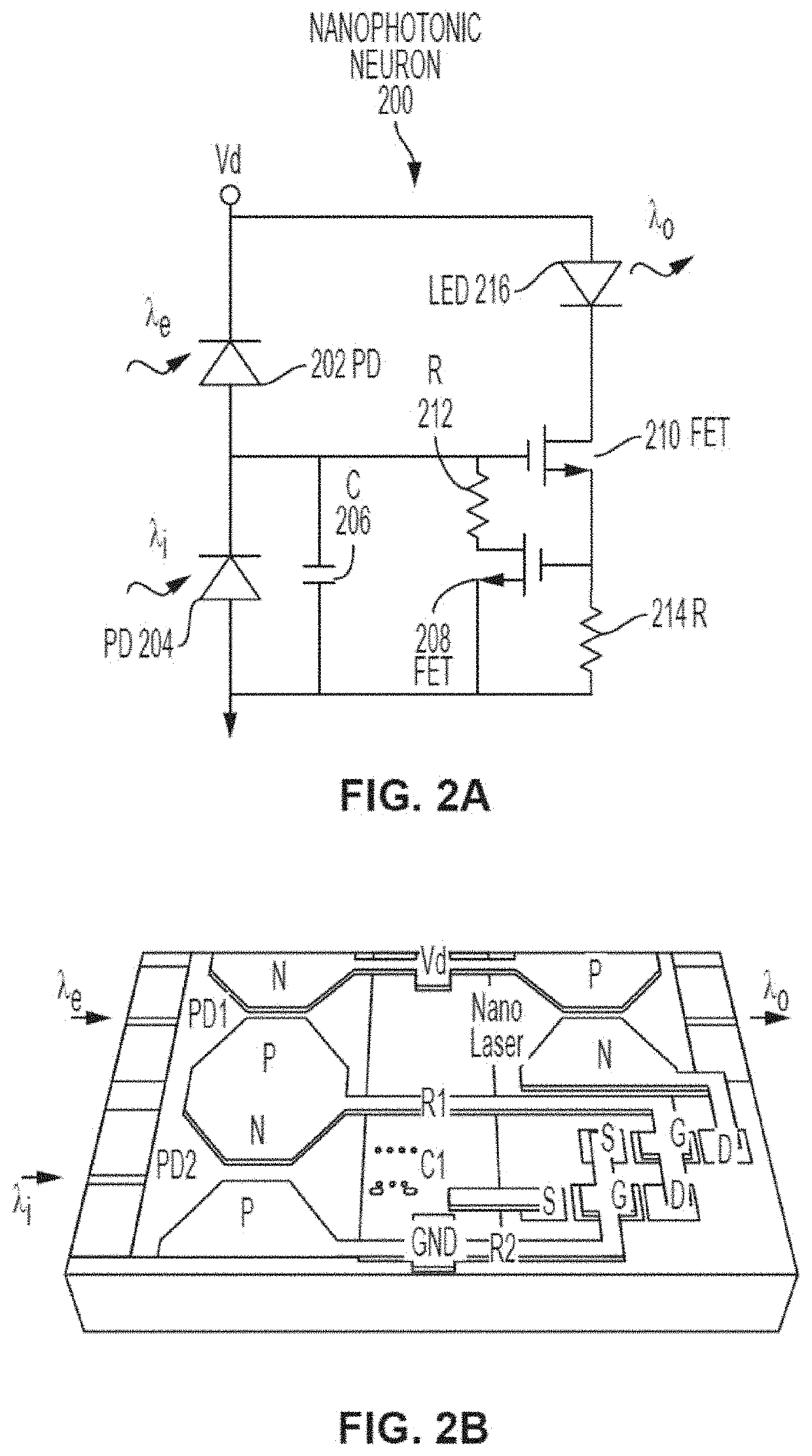
Parallel architectures for nanophotonic computing
PatentPendingUS20220044100A1
Innovation
- A nanophotonic computing system with arrayed-waveguide grating routers and phase modulators that enable cyclic, all-to-all routing and adjustable synaptic weights, allowing for arbitrary weight values between nanophotonic neurons through optical path length adjustments, facilitating high parallelism and energy efficiency.
Energy Efficiency Considerations
Energy efficiency represents a critical factor in the development and scaling of photonic interconnects for multi-chip neuromorphic systems. Traditional electronic interconnects face significant energy constraints when operating at high data rates, with power consumption increasing exponentially as bandwidth requirements grow. Photonic interconnects offer substantial advantages in this domain, with theoretical energy consumption as low as 1-10 fJ/bit compared to 10-100 pJ/bit for electronic counterparts, representing a potential 1000x improvement in energy efficiency.
The energy profile of photonic interconnects stems from their fundamental operating principles. Unlike electronic interconnects that suffer from RC delays and capacitive loading, optical signals propagate with minimal loss and dispersion through waveguides. This physical advantage translates directly to reduced power requirements for signal transmission across chip boundaries. Current state-of-the-art silicon photonic modulators operate at approximately 50-100 fJ/bit, while germanium photodetectors achieve similar efficiency metrics, demonstrating the practical realization of these theoretical advantages.
When scaling to multi-chip neuromorphic systems, the energy efficiency benefits become even more pronounced. Neuromorphic architectures typically require massive interconnectivity between processing elements, creating communication bottlenecks that can dominate system power consumption. Wavelength division multiplexing (WDM) in photonic interconnects enables parallel data transmission without proportional increases in power consumption, addressing this challenge effectively. Recent demonstrations have shown 16-channel WDM links operating at aggregate bandwidths exceeding 1 Tb/s while maintaining energy efficiency below 1 pJ/bit.
Thermal considerations also play a crucial role in the energy efficiency equation. Photonic components exhibit temperature sensitivity that can affect performance and reliability. Advanced thermal management techniques, including localized temperature control and athermal device designs, have emerged to address these challenges. These approaches typically add 10-20% overhead to the total energy budget but ensure stable operation across varying environmental conditions.
Looking forward, emerging technologies promise to further enhance energy efficiency in photonic neuromorphic systems. Phase-change materials for optical switching could reduce modulation energy to sub-femtojoule levels. Similarly, heterogeneous integration of III-V materials with silicon photonics offers pathways to ultra-efficient light sources with wall-plug efficiencies exceeding 50%. These advancements, combined with neuromorphic-specific optimizations such as spike-based communication protocols, could potentially drive system-level energy efficiency below 100 aJ/bit-operation, enabling truly scalable brain-inspired computing architectures.
Manufacturing Scalability Challenges
The manufacturing scalability of photonic interconnects represents a critical bottleneck in the widespread adoption of multi-chip neuromorphic systems. Current fabrication processes for integrated photonics face significant yield challenges when scaling to large volumes required for commercial neuromorphic computing applications. Silicon photonics manufacturing, while leveraging existing CMOS infrastructure, still struggles with waveguide loss variations and coupling efficiency inconsistencies that dramatically impact system performance at scale.
Material compatibility issues further complicate manufacturing scalability. The integration of different materials—silicon, silicon nitride, III-V semiconductors—necessary for complete photonic interconnect functionality introduces thermal expansion mismatches and interface defects. These challenges are particularly pronounced when transitioning from laboratory demonstrations to high-volume manufacturing environments, where process control must be maintained across thousands of devices with nanometer-scale precision.
Packaging and assembly present another dimension of manufacturing complexity. The alignment tolerance for optical coupling between chips typically requires sub-micron precision, orders of magnitude more demanding than traditional electronic packaging. Current solutions rely heavily on active alignment techniques that are inherently time-consuming and expensive, creating a significant barrier to cost-effective mass production of multi-chip neuromorphic systems with photonic interconnects.
Testing methodologies for photonic interconnects at scale remain underdeveloped compared to their electronic counterparts. The lack of standardized, high-throughput optical testing infrastructure increases manufacturing costs and cycle times. Wafer-level testing of photonic components is particularly challenging, as optical access to devices often requires specialized probe configurations that are difficult to implement in production environments.
Supply chain limitations further constrain manufacturing scalability. The ecosystem for photonic components remains fragmented, with specialized suppliers for lasers, modulators, detectors, and passive components. This fragmentation leads to integration challenges and potential bottlenecks in component availability that can disrupt production scaling efforts for neuromorphic systems.
Cost structures for photonic manufacturing currently do not benefit from the same economies of scale as electronic components. The specialized equipment, materials, and expertise required for photonic fabrication maintain high per-unit costs even as volumes increase. Achieving the cost targets necessary for widespread adoption of neuromorphic computing will require significant innovations in manufacturing processes and equipment to reduce these structural cost barriers.
Unlock deeper insights with Patsnap Eureka Quick Research — get a full tech report to explore trends and direct your research. Try now!
Generate Your Research Report Instantly with AI Agent
Supercharge your innovation with Patsnap Eureka AI Agent Platform!