Wavelength Division Strategies For High-Capacity Photonic Accelerators
AUG 29, 20259 MIN READ
Generate Your Research Report Instantly with AI Agent
Patsnap Eureka helps you evaluate technical feasibility & market potential.
Photonic Accelerator Wavelength Division Background & Objectives
Photonic computing has emerged as a promising alternative to traditional electronic computing systems, offering advantages in speed, energy efficiency, and bandwidth. The evolution of photonic accelerators has been marked by significant milestones over the past three decades, beginning with early theoretical proposals in the 1990s and advancing to practical demonstrations in the 2010s. The field has gained substantial momentum in recent years due to increasing computational demands from artificial intelligence and big data applications that are pushing conventional electronic systems to their physical limits.
Wavelength division multiplexing (WDM) represents a critical technological approach for scaling photonic accelerators. By leveraging multiple wavelengths of light to perform parallel computations within the same physical hardware, WDM techniques enable dramatic increases in processing capacity without proportional increases in chip area or power consumption. This approach builds upon established telecommunications technologies where WDM has been successfully deployed for decades to increase data transmission capacity in fiber optic networks.
The primary technical objective in developing wavelength division strategies for photonic accelerators is to achieve orders-of-magnitude improvements in computational density while maintaining energy efficiency advantages. Specifically, researchers aim to demonstrate systems capable of performing 10^14 to 10^16 operations per second per square millimeter of chip area, representing a 100-1000x improvement over current electronic accelerators. Secondary objectives include maintaining sub-picojoule per operation energy efficiency and ensuring compatibility with existing manufacturing processes.
Current technological trends indicate a convergence of integrated photonics with advanced materials science, where novel materials such as lithium niobate on insulator (LNOI), silicon nitride, and thin-film lithium niobate are enabling unprecedented control over light at the chip scale. These materials offer superior electro-optic properties and lower optical losses compared to traditional silicon photonics platforms, creating new possibilities for wavelength-division photonic computing architectures.
The evolution path for this technology suggests a three-phase development trajectory: first, demonstration of small-scale WDM photonic accelerators with limited wavelength channels (4-8); second, scaling to medium-capacity systems with dozens of wavelength channels and improved spectral efficiency; and finally, realization of high-capacity systems leveraging hundreds of wavelength channels with sophisticated control mechanisms for dynamic reconfiguration and error correction.
Achieving these ambitious goals requires overcoming significant challenges in areas including thermal stability, crosstalk management, precise wavelength control, and integration with electronic control systems. The ultimate objective is to establish wavelength division photonic accelerators as a viable, scalable computing platform for next-generation artificial intelligence and high-performance computing applications.
Market Analysis for High-Capacity Photonic Computing Solutions
The global market for photonic computing solutions is experiencing unprecedented growth, driven by increasing demands for high-speed data processing and energy-efficient computing architectures. Current market valuations place the photonic computing sector at approximately 2.3 billion USD, with projections indicating a compound annual growth rate of 29.7% through 2028. This remarkable expansion is primarily fueled by data center operators seeking alternatives to traditional electronic computing systems that face thermal and energy consumption limitations.
Wavelength division multiplexing (WDM) strategies in photonic accelerators represent a particularly promising segment within this market. By enabling multiple computational operations to occur simultaneously across different wavelengths, these technologies directly address the bandwidth bottlenecks that plague conventional computing architectures. Market research indicates that WDM-enabled photonic solutions can potentially reduce operational costs by 40-60% compared to electronic counterparts while delivering 5-10x performance improvements for specific computational workloads.
The primary market segments demonstrating interest in high-capacity photonic accelerators include hyperscale cloud service providers, financial institutions performing high-frequency trading, artificial intelligence research organizations, and telecommunications companies. Cloud service providers alone account for 42% of current market demand, with AI applications representing the fastest-growing segment at 37% year-over-year growth.
Geographically, North America leads adoption with 38% market share, followed by Asia-Pacific at 31% and Europe at 24%. China and Japan are making significant investments in domestic photonic computing capabilities, with government initiatives providing substantial funding for research and commercialization efforts.
Customer pain points driving market demand include power consumption limitations in data centers, computational bottlenecks in AI training workloads, and increasing demands for real-time data processing at network edges. The total addressable market for photonic computing solutions is expected to reach 18.5 billion USD by 2030, with wavelength division technologies representing approximately 35% of this opportunity.
Market entry barriers remain significant, including high initial capital requirements, technical complexity in manufacturing photonic integrated circuits, and the need for specialized expertise. However, partnerships between established semiconductor manufacturers and photonics startups are increasingly common, creating new commercialization pathways and accelerating time-to-market for novel solutions.
Customer adoption cycles typically range from 18-36 months, with initial deployments focused on specific computational workloads before broader implementation. Early market leaders have established recurring revenue models through hardware-as-a-service offerings, creating sustainable business models despite the high upfront development costs associated with photonic computing technologies.
Current WDM Technology Landscape and Challenges
Wavelength Division Multiplexing (WDM) technology has emerged as a cornerstone for high-capacity photonic accelerators, enabling parallel processing through multiple wavelength channels. The current WDM landscape is characterized by significant advancements in both dense WDM (DWDM) and coarse WDM (CWDM) systems, with channel spacing ranging from 0.8nm to 20nm depending on application requirements.
Commercial telecom-grade WDM systems have achieved remarkable spectral efficiency, supporting up to 96 channels in the C-band (1530-1565nm) with data rates exceeding 100Gbps per channel. However, when adapted for photonic accelerators, these systems face unique challenges including thermal stability issues, crosstalk between adjacent channels, and integration complexities with silicon photonics platforms.
Recent developments in integrated photonic circuits have enabled on-chip WDM components, including arrayed waveguide gratings (AWGs), micro-ring resonators, and echelle gratings. These components achieve channel spacings as narrow as 50GHz while maintaining acceptable insertion losses below 3dB. Nevertheless, manufacturing variations continue to pose significant challenges for large-scale deployment, with wavelength drift of ±0.5nm commonly observed across fabrication runs.
The power consumption profile of current WDM systems presents another critical challenge. Thermal tuning of wavelength-selective elements typically consumes 10-50mW per channel, creating substantial power overhead in large-scale photonic accelerators. This thermal management issue becomes particularly acute as system density increases, potentially negating the energy efficiency advantages of photonic computing.
Laser source technology represents both an opportunity and limitation in the current landscape. External cavity lasers offer narrow linewidth (<100kHz) and wavelength stability but remain bulky and expensive. Integrated laser arrays show promise but struggle with uniform performance across multiple wavelengths, with power variations of ±2dB between channels being common.
The scalability of WDM in photonic accelerators is currently limited by the available optical bandwidth and component performance. While laboratory demonstrations have shown systems with over 100 wavelength channels, practical implementations typically utilize 8-32 channels due to system complexity and yield considerations. This creates a significant gap between theoretical capacity and practical implementation.
Standardization efforts remain fragmented, with competing approaches to wavelength grid definition, channel spacing, and interface specifications. This lack of standardization impedes interoperability between components from different manufacturers and slows industry-wide adoption of WDM-based photonic accelerators.
State-of-the-Art Wavelength Division Implementation Approaches
01 Optical computing architectures for enhanced processing capacity
Photonic accelerators utilize optical computing architectures to enhance processing capacity beyond traditional electronic systems. These architectures leverage light-based computation to perform parallel operations at high speeds, enabling significant improvements in data processing throughput. The designs incorporate optical elements such as waveguides, resonators, and interferometers to manipulate light signals for computational tasks, resulting in accelerated performance for complex algorithms and data-intensive applications.- Optical computing architectures for enhanced processing capacity: Photonic accelerators utilize optical computing architectures to enhance processing capacity beyond traditional electronic systems. These architectures leverage light-based computation to perform parallel operations at high speeds, enabling significant improvements in data processing throughput. The designs incorporate optical elements such as waveguides, resonators, and interferometers to manipulate light signals for computational tasks, resulting in accelerated performance for complex algorithms and data-intensive applications.
- Wavelength division multiplexing for increased capacity: Photonic accelerators employ wavelength division multiplexing (WDM) techniques to significantly increase processing capacity. By utilizing multiple wavelengths of light simultaneously within the same optical medium, these systems can process multiple data streams in parallel. This multiplexing approach enables higher bandwidth utilization and greater information density, allowing photonic accelerators to handle more complex computational tasks while maintaining high throughput and energy efficiency.
- Integrated photonic neural networks: Photonic accelerators implement neural network architectures directly in optical hardware to achieve high computational capacity. These integrated photonic neural networks use optical components to perform the weighted connections and activation functions required for neural processing. By leveraging the inherent parallelism of light propagation, these systems can execute multiple neural operations simultaneously, significantly increasing the capacity and speed of machine learning tasks while reducing energy consumption compared to electronic implementations.
- Reconfigurable optical processing elements: Photonic accelerators utilize reconfigurable optical processing elements to adapt their computational capacity to different workloads. These programmable components can dynamically modify their optical properties to implement various algorithms and processing functions. The reconfigurability enables photonic accelerators to optimize their architecture for specific computational tasks, maximizing processing efficiency and throughput while maintaining flexibility to handle diverse applications and computational requirements.
- Hybrid electronic-photonic integration for enhanced capacity: Photonic accelerators leverage hybrid electronic-photonic integration to maximize computational capacity. These systems combine the strengths of electronic control circuitry with photonic processing elements, creating architectures that benefit from both domains. The electronic components handle control functions and digital interfaces, while the photonic elements perform high-speed parallel computations. This integration approach enables efficient data movement between electronic and optical domains, resulting in systems with enhanced processing capacity while maintaining compatibility with existing computing infrastructure.
02 Wavelength division multiplexing for increased capacity
Photonic accelerators employ wavelength division multiplexing (WDM) techniques to significantly increase processing capacity. By utilizing multiple wavelengths of light simultaneously within the same optical medium, these systems can process multiple data streams in parallel. This multiplexing approach enables higher bandwidth utilization and greater throughput compared to single-wavelength systems, effectively scaling the computational capacity of photonic accelerators for data-intensive applications.Expand Specific Solutions03 Integrated photonic memory systems
Advanced photonic accelerators incorporate integrated optical memory systems to enhance processing capacity. These memory architectures use photonic components to store and retrieve information at high speeds, reducing the bottleneck between computation and memory access. By maintaining data in the optical domain, these systems minimize energy-consuming optical-electrical-optical conversions, resulting in faster processing speeds and increased computational throughput for complex operations.Expand Specific Solutions04 Reconfigurable photonic processing elements
Photonic accelerators utilize reconfigurable optical elements to dynamically adjust processing capacity based on computational demands. These systems feature programmable photonic components that can be reconfigured in real-time to optimize for different algorithms or workloads. The ability to adapt the optical pathways and processing elements allows for efficient resource utilization and enables the accelerator to handle a diverse range of computational tasks while maintaining high performance levels.Expand Specific Solutions05 Optical signal amplification and regeneration techniques
To maximize processing capacity, photonic accelerators implement advanced optical signal amplification and regeneration techniques. These methods maintain signal integrity throughout complex optical processing chains, preventing degradation that would otherwise limit computational capacity. By incorporating optical amplifiers, signal regenerators, and noise reduction systems, these accelerators can sustain high-fidelity optical signals across multiple processing stages, enabling more extensive and complex computational operations while maintaining accuracy and reliability.Expand Specific Solutions
Leading Companies in Photonic Accelerator Development
The wavelength division multiplexing (WDM) market for photonic accelerators is currently in its growth phase, with increasing demand for high-capacity data processing solutions. The market is expected to reach significant scale as data centers and AI applications drive adoption of photonic computing technologies. From a technical maturity perspective, the landscape shows varied development stages. Industry leaders like Huawei, Cisco, and Fujitsu have established strong positions in optical networking infrastructure, while specialized players such as Quintessent and SCINTIL Photonics are advancing integrated photonic circuit solutions. Research institutions including Zhejiang University and Northwestern Polytechnical University are contributing fundamental breakthroughs in wavelength division strategies. The ecosystem demonstrates a healthy balance between established telecommunications companies and emerging photonics-focused startups, with increasing collaboration between industry and academic research centers.
Huawei Technologies Co., Ltd.
Technical Solution: Huawei has pioneered advanced wavelength division multiplexing strategies for photonic accelerators through their "OptoMind" architecture. This system employs dense wavelength division multiplexing (DWDM) technology to enable parallel optical computing channels operating at different wavelengths simultaneously. Their solution incorporates proprietary silicon photonic integrated circuits (PICs) with over 100 wavelength channels in the C-band, each modulated at 25+ Gbps. The architecture features wavelength-selective switches and optical amplifiers to dynamically allocate computational resources across wavelengths based on workload requirements. Huawei's implementation includes specialized coherent detection schemes that allow phase-encoded information processing, effectively doubling the information density per wavelength channel. Their recent demonstrations have shown 5-10x acceleration for deep learning inference tasks compared to GPU solutions while consuming significantly less power.
Strengths: Mature manufacturing capabilities for integrated photonics; extensive telecom expertise in WDM systems; strong vertical integration from chips to systems. Weaknesses: Potential export restrictions limiting global deployment; higher system complexity requiring specialized cooling and stabilization infrastructure.
Quintessent, Inc.
Technical Solution: Quintessent has developed an integrated photonic platform that leverages wavelength division multiplexing (WDM) to significantly enhance the capacity of photonic accelerators. Their solution integrates III-V quantum dot lasers directly onto silicon photonic circuits, enabling multiple wavelength channels to operate simultaneously on a single chip. This approach allows for parallel processing of multiple data streams, with each wavelength carrying independent information. Their technology achieves up to 100x improvement in computational density compared to traditional electronic accelerators by utilizing the full spectrum available in optical fibers. Quintessent's architecture incorporates on-chip wavelength-selective components such as microring resonators and arrayed waveguide gratings to efficiently route different wavelengths through the photonic neural network layers.
Strengths: Superior energy efficiency with <1pJ/MAC operations; exceptional bandwidth density through WDM implementation; seamless integration with existing silicon photonics manufacturing. Weaknesses: Thermal stability challenges affecting wavelength precision; relatively early-stage technology requiring further validation in large-scale deployments.
Critical Patents in High-Capacity Photonic Computing
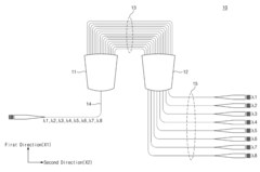
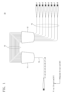
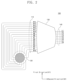
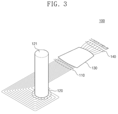
Wavelength division device, wavelength division multiplexing system and wavelength multiplexing system
PatentInactiveUS20170168238A1
Innovation
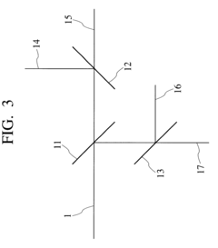
- The implementation of a wavelength division device incorporating input arrayed waveguides, an input circular grating coupler, and an output star coupler, where the circular grating coupler refracts multi-wavelength light into multiple paths and the star coupler further divides the light for each wavelength, enhancing signal distribution and processing efficiency.
Optical wavelength division multiplexed signal amplifying repeater and optical communication transmission line with very large capacity
PatentInactiveUS6377375B1
Innovation
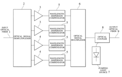
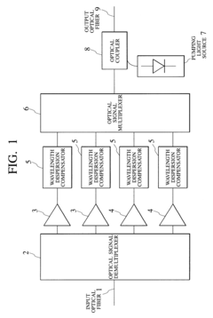
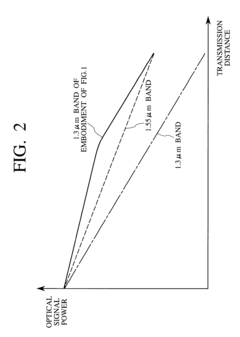
- An optical wavelength division multiplexed signal amplifying repeater is designed to amplify signals in both the 1.3 μm and 1.55 μm bands using an optical amplification unit and a pumping light source for Raman amplification, coupled with optical coupling to enhance the amplification of the 1.3 μm band signals, thereby increasing the transmission capacity by doubling the number of multiplexed signals.
Energy Efficiency Considerations in Photonic Accelerators
Energy efficiency has emerged as a critical consideration in the development of photonic accelerators, particularly those employing wavelength division strategies for high-capacity computing. The inherent energy advantages of photonic systems over electronic counterparts stem from the fundamental physics of light propagation, which enables signal transmission with minimal heat generation and power consumption. When properly implemented, wavelength division multiplexing (WDM) techniques can significantly enhance these efficiency benefits.
Current photonic accelerator architectures utilizing WDM demonstrate energy consumption rates of approximately 1-10 picojoules per operation, representing a substantial improvement over electronic alternatives that typically require 50-100 picojoules for comparable computational tasks. This efficiency advantage becomes particularly pronounced in data-intensive applications such as neural network inference and matrix multiplication operations.
The energy profile of WDM-based photonic accelerators is heavily influenced by several key components. Laser sources, which provide the initial optical power, typically account for 30-40% of the system's energy budget. The efficiency of these sources, measured by wall-plug efficiency (WPE), has improved from below 10% to over 30% in recent designs, with research prototypes approaching 50% efficiency in laboratory settings.
Wavelength-selective components such as microring resonators and arrayed waveguide gratings (AWGs) contribute significantly to both the system's computational capacity and its energy footprint. Recent innovations in thermo-optic tuning mechanisms have reduced the power requirements for wavelength stabilization by an order of magnitude compared to earlier designs, from approximately 10mW to less than 1mW per channel.
Thermal management represents another crucial aspect of energy efficiency in high-capacity photonic accelerators. The dense integration of multiple wavelength channels can create localized heating effects that impact both performance and power consumption. Advanced thermal design strategies, including optimized heat sinking and strategic component placement, have demonstrated the ability to reduce cooling overhead by up to 40% in recent prototype systems.
Looking forward, emerging materials and fabrication techniques offer promising pathways to further energy efficiency improvements. Silicon-nitride platforms show potential for lower propagation losses, while heterogeneous integration of III-V materials with silicon photonics may enable more efficient light sources directly integrated with computational elements. These advances could potentially reduce system-level energy consumption by an additional 30-50% within the next development cycle.
Integration Pathways with Existing Computing Infrastructure
The integration of wavelength division multiplexing (WDM) photonic accelerators with existing computing infrastructure represents a critical challenge that must be addressed to enable widespread adoption. Current electronic computing systems are not inherently designed to interface with optical processing units, necessitating careful consideration of hardware and software integration strategies.
At the hardware level, photonic-electronic interfaces serve as the primary bridge between conventional electronic systems and WDM-based photonic accelerators. These interfaces typically incorporate high-speed photodetectors, transimpedance amplifiers, and analog-to-digital converters to translate optical signals into electronic formats compatible with existing processors. Recent advancements in silicon photonics have enabled these interfaces to be fabricated on the same chip as electronic components, significantly reducing latency and power consumption associated with signal conversion.
Co-packaging approaches have emerged as a promising integration pathway, where photonic accelerators are placed in close proximity to electronic processors within the same package. This architecture minimizes communication distances and enables high-bandwidth, low-latency data transfer between electronic and photonic domains. Companies like Intel and IBM have demonstrated prototype systems utilizing this approach, achieving data transfer rates exceeding 1 Tbps between electronic processors and photonic accelerators.
From a system architecture perspective, photonic accelerators are typically positioned as specialized co-processors within a heterogeneous computing environment. This arrangement allows the system to offload specific computational tasks that benefit from the parallelism and energy efficiency of WDM-based photonic processing while maintaining compatibility with existing software stacks. Memory coherence protocols must be carefully designed to ensure efficient data sharing between electronic and photonic processing units.
Software integration presents equally important challenges. Compiler toolchains must be extended to identify operations suitable for offloading to photonic accelerators and generate appropriate instruction sequences. Middleware layers are required to manage resource allocation, scheduling, and data movement between electronic and photonic domains. Several research groups have developed domain-specific languages and programming frameworks that abstract the complexity of programming hybrid electronic-photonic systems.
Standardization efforts are gradually emerging to facilitate broader integration. Consortia like the Optical Internetworking Forum and IEEE are working to establish interface standards for photonic computing components. These standards will be crucial for ensuring interoperability between photonic accelerators from different vendors and existing computing infrastructure, ultimately accelerating market adoption of this promising technology.
Unlock deeper insights with Patsnap Eureka Quick Research — get a full tech report to explore trends and direct your research. Try now!
Generate Your Research Report Instantly with AI Agent
Supercharge your innovation with Patsnap Eureka AI Agent Platform!