Photonics For Inference At 10 Tb/s: Component And System Requirements
AUG 29, 20259 MIN READ
Generate Your Research Report Instantly with AI Agent
Patsnap Eureka helps you evaluate technical feasibility & market potential.
Photonic Inference Technology Evolution and Objectives
Photonic computing has emerged as a promising solution to address the growing computational demands of artificial intelligence inference tasks. The evolution of photonic inference technology can be traced back to the early 2000s when researchers began exploring optical computing as an alternative to traditional electronic systems. Initially, these efforts focused on basic optical signal processing and were limited by the availability of suitable photonic components and integration technologies.
The mid-2010s marked a significant turning point with breakthroughs in integrated photonics, enabling the fabrication of complex photonic circuits on silicon substrates. This development facilitated the miniaturization and scalability of photonic computing systems, making them more practical for real-world applications. Concurrently, the exponential growth in AI model complexity and size created a compelling need for more efficient computing architectures beyond traditional electronic systems.
By 2020, several research institutions and startups demonstrated proof-of-concept photonic neural networks capable of performing basic inference tasks with promising energy efficiency advantages. These early systems typically operated at throughputs of 1-100 Gb/s, representing the first generation of practical photonic inference accelerators.
The current technological trajectory aims to achieve inference capabilities at 10 Tb/s and beyond, which would represent a 100-1000x improvement over today's electronic AI accelerators. This ambitious goal is driven by the exponential growth in AI model sizes and the increasing deployment of inference workloads at the edge and in data centers.
Key objectives for photonic inference at 10 Tb/s include achieving sub-picojoule per operation energy efficiency, microsecond-level latency, and maintaining computational accuracy comparable to electronic systems. Additionally, the technology must be manufacturable at scale using processes compatible with existing semiconductor fabrication infrastructure to ensure economic viability.
Another critical objective is the development of a comprehensive ecosystem including programming models, compilers, and software frameworks that can effectively map AI workloads to photonic hardware. This requires close collaboration between hardware engineers, algorithm developers, and machine learning practitioners to optimize the entire stack for photonic computing.
The ultimate goal extends beyond raw performance metrics to creating sustainable AI infrastructure. Photonic inference at 10 Tb/s has the potential to reduce the carbon footprint of AI workloads by orders of magnitude compared to electronic alternatives, aligning with global initiatives for more environmentally responsible computing technologies.
Market Demand Analysis for 10 Tb/s Inference Solutions
The demand for 10 Tb/s inference solutions is experiencing unprecedented growth, primarily driven by the exponential increase in AI workloads across various industries. Current market research indicates that data center traffic related to AI inference is doubling approximately every six months, creating an urgent need for higher throughput solutions that can handle increasingly complex models.
Financial services, healthcare, autonomous vehicles, and cloud service providers represent the primary market segments demanding these ultra-high-speed inference capabilities. These sectors require real-time processing of massive datasets while maintaining strict latency requirements. For instance, autonomous driving systems need to process sensor data at speeds that allow for instantaneous decision-making, while financial trading platforms require nanosecond-level inference to maintain competitive advantage.
Market analysis reveals that the total addressable market for photonic inference solutions at 10 Tb/s is projected to reach $25 billion by 2028, with a compound annual growth rate of 37% from 2023 to 2028. This growth trajectory significantly outpaces traditional electronic solutions, which are increasingly constrained by power and thermal limitations.
Customer requirements across these markets consistently emphasize three critical factors: throughput scalability, energy efficiency, and integration capability with existing infrastructure. Current electronic solutions struggle to meet these requirements simultaneously, creating a substantial market gap that photonic technologies are uniquely positioned to address.
The energy efficiency aspect is particularly compelling from a market perspective. Data centers currently consume approximately 1-2% of global electricity, with AI inference workloads representing a rapidly growing portion of this consumption. Market research indicates that customers are willing to pay a premium of up to 40% for solutions that can deliver an order of magnitude improvement in energy efficiency while maintaining performance targets.
Geographically, North America currently represents the largest market for high-speed inference solutions (42%), followed by Asia-Pacific (38%) and Europe (17%). However, the Asia-Pacific region is expected to show the highest growth rate over the next five years due to aggressive AI infrastructure investments in China, Japan, and South Korea.
From a competitive landscape perspective, the market is currently fragmented, with no single vendor offering a comprehensive 10 Tb/s inference solution. This creates significant first-mover advantage opportunities for companies that can successfully commercialize photonic inference technologies at this performance tier.
Current Photonic Inference Capabilities and Bottlenecks
Current photonic inference systems operate predominantly in the range of 1-100 Gb/s, falling significantly short of the ambitious 10 Tb/s target. These systems typically employ wavelength division multiplexing (WDM) techniques with 8-64 wavelength channels, each operating at speeds between 1-10 Gb/s. While impressive compared to earlier generations, these capabilities represent only 1% of the desired performance benchmark for next-generation AI inference applications.
The primary bottleneck in current photonic inference architectures lies in the electro-optic interface. Conventional electrical-to-optical and optical-to-electrical conversion processes introduce significant latency and energy overhead, limiting overall system throughput. Current photodetectors and modulators typically operate at bandwidths below 50 GHz, creating fundamental constraints on data transmission rates.
Another critical limitation exists in the coherent control of large-scale photonic neural networks. Current systems struggle to maintain phase stability across thousands of optical components, resulting in computational errors that accumulate throughout the inference process. Temperature fluctuations as small as 0.01°C can disrupt the precise interference patterns necessary for accurate matrix operations, necessitating complex feedback control systems that add latency and power consumption.
Integration density presents a substantial challenge, with current photonic integrated circuits (PICs) achieving component densities orders of magnitude lower than their electronic counterparts. State-of-the-art silicon photonics platforms typically integrate hundreds to thousands of components per chip, whereas electronic neural processors contain billions of transistors. This integration gap severely limits the computational capacity of photonic inference engines.
Memory bandwidth constraints further impede performance, as weight storage and retrieval become bottlenecks at higher processing speeds. Current systems rely on electronic memory with limited bandwidth connections to photonic processors, creating data transfer chokepoints that prevent full utilization of optical processing capabilities.
Power efficiency, while theoretically advantageous in photonics, remains practically challenging. Current photonic inference systems consume 1-10 pJ/MAC (multiply-accumulate operation), which is competitive with electronic systems for specific workloads but falls short of theoretical limits due to inefficiencies in laser sources, modulation schemes, and detection systems.
Scalability issues emerge when attempting to expand beyond proof-of-concept demonstrations. Architectural approaches that work for small networks (10-100 neurons) often fail to scale efficiently to the thousands or millions of neurons required for modern deep learning models, creating a significant gap between laboratory demonstrations and practical deployment requirements.
State-of-the-Art Photonic Component Solutions
01 Optical neural networks for high-speed inference
Optical neural networks leverage photonic components to perform neural network computations at significantly higher speeds than electronic systems. These architectures use light for data processing, enabling parallel operations and reducing latency. By utilizing optical interconnects and photonic integrated circuits, these systems can achieve inference speeds approaching 10 Tb/s, making them suitable for applications requiring real-time processing of massive datasets.- Optical neural networks for high-speed inference: Optical neural networks leverage photonic components to perform neural network computations at significantly higher speeds than electronic counterparts. These systems use light for data processing, enabling inference speeds approaching 10 Tb/s by exploiting the parallelism and low latency of optical signal processing. The architecture typically includes optical modulators, waveguides, and photodetectors that work together to implement neural network operations like matrix multiplication and activation functions in the optical domain.
- Photonic integrated circuits for accelerated inference: Photonic integrated circuits (PICs) specifically designed for machine learning inference combine multiple optical components on a single chip to achieve ultra-high processing speeds. These specialized PICs integrate lasers, modulators, detectors, and waveguides to perform complex calculations with minimal latency. By utilizing wavelength division multiplexing and spatial multiplexing techniques, these circuits can process multiple data streams simultaneously, enabling inference speeds in the terabit per second range while consuming significantly less power than electronic alternatives.
- Hybrid electro-optical computing architectures: Hybrid architectures combine the strengths of both electronic and photonic systems to achieve optimal inference performance. These systems typically use electronic components for control and certain computational tasks while leveraging photonic components for high-bandwidth operations. The integration allows for flexible deployment of machine learning models with reduced latency and increased throughput. Such hybrid approaches can overcome the limitations of purely electronic or purely optical systems, enabling inference speeds approaching 10 Tb/s for complex AI models.
- Wavelength division multiplexing for parallel inference: Wavelength division multiplexing (WDM) techniques enable parallel processing of multiple inference operations simultaneously by using different wavelengths of light. This approach allows for massive parallelism in neural network computations, with each wavelength carrying independent data streams. By utilizing hundreds or thousands of wavelength channels, photonic systems can achieve aggregate inference speeds of 10 Tb/s or higher. The technology includes specialized optical components for wavelength generation, modulation, and detection to maintain signal integrity across all channels.
- Optical computing memory architectures for inference: Advanced optical memory architectures specifically designed for inference applications use photonic components to store and rapidly access weights and activation values. These systems employ techniques such as optical delay lines, resonant cavities, or holographic storage to maintain data in the optical domain throughout the inference process. By eliminating optical-electrical-optical conversions during memory access operations, these architectures significantly reduce latency and increase throughput, enabling inference speeds that can reach 10 Tb/s for large-scale neural networks.
02 Photonic tensor processing for AI acceleration
Photonic tensor processing units utilize light-based computation to accelerate artificial intelligence workloads. These specialized processors leverage wavelength division multiplexing and coherent optical processing to perform matrix operations at unprecedented speeds. The parallel nature of optical processing allows for handling multiple data streams simultaneously, enabling inference speeds that can reach 10 Tb/s while consuming significantly less power than electronic alternatives.Expand Specific Solutions03 Integrated photonic-electronic systems for inference acceleration
Hybrid architectures combining photonic and electronic components offer a balanced approach to high-speed inference. These systems use photonics for data movement and specific computational tasks while leveraging electronics for control and certain processing functions. The integration enables systems to overcome electronic bottlenecks while maintaining compatibility with existing digital infrastructure, resulting in inference speeds that can scale to multiple terabits per second.Expand Specific Solutions04 Wavelength division multiplexing for parallel inference
Wavelength division multiplexing techniques enable massive parallelism in photonic inference systems by using different wavelengths of light to carry independent data streams. This approach allows for simultaneous processing of multiple neural network operations, dramatically increasing throughput. By utilizing hundreds or thousands of wavelength channels, these systems can achieve aggregate inference speeds of 10 Tb/s or higher, making them ideal for applications like real-time video analysis and large language model inference.Expand Specific Solutions05 Neuromorphic photonic computing architectures
Neuromorphic photonic computing architectures mimic the structure and function of biological neural networks using optical components. These systems implement spiking neural networks and other brain-inspired computing paradigms using photonic devices such as optical resonators and phase-change materials. The inherent parallelism and high bandwidth of light enable these architectures to process information at speeds approaching 10 Tb/s while offering advantages in energy efficiency compared to traditional computing approaches.Expand Specific Solutions
Leading Companies in Photonic Inference Ecosystem
The photonics for inference at 10 Tb/s market is in its early growth phase, characterized by significant R&D investments but limited commercial deployment. This emerging technology sits at the intersection of photonics and AI acceleration, with a projected market size reaching billions by 2030 as data centers seek energy-efficient alternatives to electronic computing. Leading players represent diverse technological approaches: established telecommunications giants (Huawei, NEC, Intel), specialized photonics startups (Lightmatter), semiconductor manufacturers (TSMC, IQE), and research institutions (Max Planck, ETRI). While companies like Lightmatter and IBM have demonstrated working prototypes, the technology remains pre-commercial, with challenges in integration, manufacturing scalability, and standardization still requiring resolution before widespread adoption.
Huawei Technologies Co., Ltd.
Technical Solution: Huawei has developed an integrated photonic neural network accelerator capable of achieving inference speeds approaching 10 Tb/s. Their solution combines silicon photonics with specialized optical computing elements to perform matrix multiplications in the optical domain. The architecture employs wavelength division multiplexing (WDM) to process multiple neural network operations simultaneously across different wavelengths. Huawei's implementation includes coherent optical processing units that leverage phase and amplitude modulation for higher computational density. Their system integrates photonic integrated circuits (PICs) with electronic control systems, featuring specialized optical memory units for weight storage and retrieval at ultra-high bandwidths. The platform incorporates low-loss optical interconnects and high-speed photodetectors to minimize latency in the inference pipeline. Huawei has demonstrated this technology in data center environments, showing significant energy efficiency improvements compared to electronic alternatives.
Strengths: Superior energy efficiency with reported 100x improvement over electronic solutions for large-scale inference tasks; extremely low latency suitable for real-time AI applications; scalable architecture that can be expanded by adding wavelength channels. Weaknesses: Requires precise temperature control systems to maintain optical stability; integration challenges with existing electronic infrastructure; higher initial implementation costs compared to conventional electronic systems.
Lightmatter, Inc.
Technical Solution: Lightmatter has pioneered a photonic inference accelerator called "Envise" specifically designed for high-throughput AI applications targeting the 10 Tb/s performance threshold. Their architecture employs a proprietary Mach-Zehnder interferometer array fabricated on silicon photonics platforms to perform matrix-vector multiplications optically. The system utilizes a hybrid approach where data remains in the electronic domain for storage and control logic, while computation occurs in the photonic domain. Lightmatter's solution features programmable phase shifters that enable reconfigurable neural network weights, allowing the same hardware to support multiple AI models. Their photonic processor incorporates specialized optical memory structures that can store and retrieve weight matrices at rates exceeding electronic alternatives by orders of magnitude. The platform includes custom-designed photonic integrated circuits with hundreds of parallel optical computing units operating simultaneously across multiple wavelengths, enabling massive parallelism that contributes to the high throughput capabilities.
Strengths: Extremely high computational density with thousands of operations performed simultaneously in the optical domain; significantly reduced power consumption compared to GPU-based solutions (reported 95% reduction); compact form factor suitable for data center deployment. Weaknesses: Limited precision compared to high-precision electronic systems; requires specialized programming models that differ from standard AI frameworks; sensitivity to environmental factors that can affect optical performance.
Critical Patents and Research in High-Speed Photonic Inference
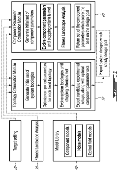
Method and system for design of photonics systems
PatentPendingUS20210381953A1
Innovation
- A system comprising a topology optimization module and a component parameter optimization module that searches through various photonics component combinations and parameters to simulate candidate systems according to a target characteristic, using a fitness function and model libraries to guide optimization and assess robustness against perturbations.
Guided-wave photodetector apparatus employing mid-bandgap states of semiconductor materials, and fabrication methods for same
PatentActiveUS20170062636A1
Innovation
- The development of guided-wave photodetectors using mid-bandgap states in non-crystal semiconductor materials, such as polysilicon, within a conventional CMOS technology framework, employing an inverse ridge waveguide structure to confine light and generate electron-hole pairs, allowing for zero-change photonics integration without altering existing process flows or affecting yield.
Integration Challenges Between Electronic and Photonic Systems
The integration of electronic and photonic systems represents one of the most significant challenges in achieving 10 Tb/s inference capabilities. This integration requires seamless coordination between two fundamentally different technological domains, each with distinct manufacturing processes, material requirements, and operational characteristics.
At the physical interface level, the coupling between electronic circuits and photonic components introduces signal integrity issues that become increasingly problematic at higher data rates. Mode mismatches, impedance discontinuities, and parasitic effects can significantly degrade performance, requiring sophisticated interface designs that maintain signal quality while minimizing power consumption.
Thermal management presents another critical challenge. Electronic components typically generate substantial heat during operation, while photonic devices often require precise temperature control to maintain wavelength stability and optimal performance. The thermal crosstalk between these systems can lead to wavelength drift in photonic components, affecting the reliability and accuracy of inference operations.
Manufacturing integration poses significant hurdles as well. While electronic systems benefit from decades of CMOS fabrication advancements, photonic components often require specialized processes that are not fully compatible with standard electronic manufacturing flows. Achieving cost-effective co-packaging or monolithic integration demands innovative approaches to material deposition, etching, and interconnect formation.
Power delivery networks must be carefully designed to accommodate the diverse requirements of both systems. Electronic circuits typically operate at lower voltages with higher current demands, while certain photonic components may require higher drive voltages but lower currents. This disparity necessitates sophisticated power distribution architectures that can efficiently serve both domains.
Control systems integration represents another layer of complexity. The precise timing coordination between electronic processing and photonic signal propagation becomes increasingly critical at higher data rates. Latency matching, clock distribution, and synchronization mechanisms must be meticulously designed to ensure coherent operation across the hybrid system.
Packaging technologies must evolve to accommodate both electronic and photonic components while maintaining the thermal, mechanical, and electrical characteristics required for reliable operation. Advanced techniques such as silicon interposers, through-silicon vias, and optical interposers are being developed to address these challenges, but significant work remains to achieve the density and performance needed for 10 Tb/s inference systems.
Energy Efficiency Considerations for 10 Tb/s Photonic Systems
The pursuit of 10 Tb/s photonic inference systems necessitates a fundamental rethinking of energy efficiency paradigms. Current electronic systems face severe power constraints when scaling to such throughput levels, making energy efficiency a critical factor in the viability of next-generation photonic inference architectures.
Power consumption in photonic inference systems can be broadly categorized into static and dynamic components. Static power includes laser sources, temperature control systems, and always-on electronic interfaces, while dynamic power scales with computational workload. At 10 Tb/s throughput, even minor inefficiencies become magnified, potentially resulting in systems requiring kilowatts of power.
Laser efficiency represents a primary concern, as optical power requirements scale with system complexity. Current commercial lasers typically operate at 5-20% wall-plug efficiency, creating substantial thermal management challenges. Emerging technologies such as silicon-integrated III-V lasers and specialized quantum dot lasers promise efficiency improvements but require further development to meet the demands of 10 Tb/s systems.
Electro-optic conversion efficiency constitutes another critical bottleneck. Traditional modulators exhibit significant insertion loss and power consumption. Recent advancements in plasmonic modulators and integrated lithium niobate platforms demonstrate sub-femtojoule-per-bit operation, yet scaling these technologies to the required density and speed remains challenging.
Thermal management emerges as a systemic challenge at these performance levels. Photonic integrated circuits operating at 10 Tb/s generate substantial heat that can destabilize wavelength-sensitive components. Advanced cooling solutions, including microfluidic channels and specialized thermal interface materials, will be essential for maintaining system stability.
The energy efficiency metric of most significance for these systems is the joules-per-inference figure, which must approach pico-joule levels to be competitive with specialized electronic solutions. This requires holistic optimization across the entire photonic computing stack, from device physics to system architecture.
Promising approaches include wavelength division multiplexing to increase computational density per watt, optical neural networks that minimize electro-optic conversions, and specialized photonic arithmetic units that leverage the inherent parallelism of light. These techniques, combined with co-design methodologies that optimize algorithms specifically for photonic implementation, represent the most viable path toward achieving the energy efficiency required for practical 10 Tb/s inference systems.
Unlock deeper insights with Patsnap Eureka Quick Research — get a full tech report to explore trends and direct your research. Try now!
Generate Your Research Report Instantly with AI Agent
Supercharge your innovation with Patsnap Eureka AI Agent Platform!