On-Chip Photonic Coherence Management For Large-Scale Arrays
AUG 29, 202510 MIN READ
Generate Your Research Report Instantly with AI Agent
Patsnap Eureka helps you evaluate technical feasibility & market potential.
Photonic Coherence Technology Background and Objectives
Photonic coherence management represents a critical frontier in integrated photonics, evolving from early demonstrations of on-chip interferometers to today's sophisticated systems capable of manipulating light at unprecedented scales. The technology traces its origins to fundamental research in quantum optics during the 1980s and 1990s, which established theoretical frameworks for coherent light manipulation. The subsequent development of silicon photonics platforms in the early 2000s provided the necessary manufacturing infrastructure to translate these concepts into practical devices.
The evolution of this field has been characterized by progressive improvements in coherence length, stability, and scalability. Early systems were limited to managing coherence across only a few optical channels, whereas current state-of-the-art implementations can maintain phase relationships across hundreds of elements. This exponential growth in capability has paralleled advances in fabrication precision, with modern processes achieving sub-nanometer accuracy in waveguide dimensions critical for coherence preservation.
Recent technological trends indicate a convergence of multiple disciplines, including materials science, electronic control systems, and algorithmic approaches to coherence management. The integration of active phase control elements, such as thermo-optic phase shifters and electro-optic modulators, has enabled dynamic coherence manipulation essential for large-scale photonic arrays. Simultaneously, novel materials platforms including silicon nitride, lithium niobate on insulator, and thin-film lithium niobate are expanding the parameter space for coherence engineering.
The primary technical objective in this domain is to develop scalable architectures capable of maintaining optical coherence across thousands of photonic elements while minimizing power consumption, footprint, and complexity. This includes achieving phase stability better than λ/20 across the entire array under varying environmental conditions, implementing efficient calibration protocols that scale sub-linearly with array size, and developing compact feedback mechanisms for real-time coherence monitoring and correction.
Secondary objectives include enhancing the bandwidth of coherence management systems to support broadband operation, reducing crosstalk between adjacent channels to below -30 dB, and developing modular architectures that facilitate scaling from tens to thousands of elements without fundamental redesign. These capabilities would enable transformative applications in optical quantum computing, high-precision sensing, and massively parallel optical signal processing.
The ultimate goal is to establish a comprehensive technology platform that democratizes access to coherent photonic systems, allowing system designers to leverage large-scale photonic coherence without specialized expertise in the underlying physics. This would mirror the evolution of electronic integrated circuits, where complex functionality became accessible through standardized design methodologies and fabrication processes.
Market Applications for On-Chip Photonic Coherence Systems
On-chip photonic coherence management systems are poised to revolutionize multiple industries through their ability to manipulate light with unprecedented precision on integrated circuits. The telecommunications sector represents the primary market application, where these systems enable higher bandwidth optical communications by facilitating wavelength division multiplexing (WDM) with coherent detection schemes. This technology allows for dramatically increased data transmission rates while reducing power consumption in long-haul fiber networks and data center interconnects.
Quantum computing emerges as another significant application area, where maintaining photonic coherence is essential for quantum information processing. On-chip coherence management systems provide the necessary infrastructure for manipulating quantum states of light, enabling scalable photonic quantum computers that can operate at room temperature—a substantial advantage over many competing quantum technologies requiring cryogenic cooling.
The medical imaging industry stands to benefit substantially from this technology through enhanced optical coherence tomography (OCT) systems. By integrating coherence management on-chip, next-generation OCT devices can achieve higher resolution, greater depth penetration, and faster scanning rates while becoming more compact and cost-effective, revolutionizing non-invasive diagnostic capabilities.
LiDAR systems for autonomous vehicles and robotics represent another high-growth application area. On-chip coherent photonics enables frequency-modulated continuous-wave (FMCW) LiDAR with superior range resolution and immunity to environmental interference compared to traditional time-of-flight systems. The reduced size and power requirements make this technology particularly attractive for mass-market automotive applications.
Advanced manufacturing benefits from on-chip coherent photonic systems through improved metrology and quality control processes. These systems enable precise interferometric measurements at the nanoscale, critical for semiconductor manufacturing, where feature sizes continue to shrink below 5nm.
The aerospace and defense sectors utilize this technology for coherent optical radar, secure communications, and navigation systems where GPS may be unavailable. The compact form factor of on-chip solutions addresses the strict size, weight, and power constraints of aerospace applications.
Scientific instrumentation represents a specialized but growing market, with applications in spectroscopy, astronomy, and fundamental physics research. On-chip coherence management enables more sensitive detection systems for identifying chemical compounds, observing distant celestial objects, and conducting precision measurements for fundamental physical constants.
Current Challenges in Large-Scale Photonic Array Integration
Despite significant advancements in integrated photonics, large-scale photonic array integration faces several critical challenges that impede widespread commercial deployment. The primary obstacle remains maintaining coherence across extensive arrays of photonic elements. As array sizes increase beyond hundreds of elements, phase errors accumulate exponentially, degrading system performance and limiting scalability. These errors stem from fabrication variations, thermal fluctuations, and environmental instabilities that become increasingly difficult to control at larger scales.
Manufacturing precision presents another significant hurdle. Current fabrication processes struggle to maintain the nanometer-level precision required for wavelength-scale photonic structures across large chip areas. Even minor variations in waveguide dimensions or material properties can cause significant phase mismatches between array elements, disrupting coherent operation. The yield rates for large-scale photonic arrays remain prohibitively low for mass production, with defect densities increasing superlinearly with array size.
Thermal management represents a particularly challenging aspect of large-scale integration. Photonic elements are highly sensitive to temperature variations, with refractive indices changing significantly even with minor thermal fluctuations. In dense arrays, localized heating from active components creates thermal gradients that disrupt phase relationships across the array. Current on-chip thermal compensation techniques become increasingly complex and power-hungry as array dimensions grow.
Control complexity escalates dramatically with array size. Each additional photonic element requires precise phase control, typically implemented through thermo-optic or electro-optic modulators. For arrays with thousands of elements, the associated electronic control circuitry becomes unwieldy, consuming significant chip area and power. The interconnect density between photonic and electronic layers presents a bottleneck that limits practical array sizes.
Power consumption emerges as a critical limitation for large-scale arrays. Phase tuning mechanisms, particularly thermo-optic approaches, consume substantial power that scales with array size. For applications requiring continuous coherence management, such as optical beamforming or quantum information processing, power requirements can quickly become prohibitive, creating thermal management challenges that further compound coherence issues.
Integration with CMOS electronics presents additional challenges. While silicon photonics leverages existing semiconductor infrastructure, the co-integration of photonic and electronic components introduces thermal and electrical crosstalk that can disrupt coherent operation. The different optimization requirements for photonic and electronic components often lead to compromises that limit overall system performance.
AI and machine learning approaches for coherence management show promise but remain computationally intensive for real-time operation with large arrays. The development of efficient algorithms for dynamic coherence management represents an active research area with significant potential impact on large-scale photonic integration.
State-of-the-Art Coherence Management Solutions for Photonic Arrays
01 On-chip coherence management for photonic integrated circuits
Photonic integrated circuits (PICs) can incorporate on-chip coherence management systems that control and manipulate the coherence properties of light. These systems typically include coherence filters, modulators, and controllers integrated directly onto silicon or other photonic platforms. By managing coherence on-chip, these systems enable more compact and efficient optical processing for applications in telecommunications, sensing, and quantum computing.- Integrated photonic coherence management systems: On-chip photonic coherence management systems integrate optical components onto a single semiconductor chip to control and manipulate the coherence properties of light. These systems typically include waveguides, modulators, and detectors that work together to maintain or modify coherence characteristics. The integration allows for compact, stable, and scalable solutions for applications requiring precise coherence control, such as optical communications and sensing.
- Coherence measurement and monitoring techniques: Various techniques for measuring and monitoring optical coherence in photonic integrated circuits have been developed. These include interferometric methods, spectral analysis, and phase-sensitive detection schemes that can quantify coherence length, time, and other parameters. Real-time monitoring of coherence properties enables dynamic adjustment of optical systems and compensation for environmental factors that might degrade coherence.
- Coherence control for quantum photonic applications: Specialized coherence management techniques for quantum photonic applications focus on maintaining quantum coherence properties essential for quantum information processing. These systems often incorporate cryogenic components, precise timing control, and isolation from environmental noise. The ability to maintain quantum coherence on-chip enables applications such as quantum computing, quantum key distribution, and quantum sensing with improved stability and scalability.
- Thermal and mechanical stabilization for coherence preservation: Thermal and mechanical stabilization techniques are crucial for preserving optical coherence in integrated photonic systems. These include active temperature control, vibration isolation, and specialized packaging methods that minimize environmental disturbances. By maintaining stable operating conditions, these approaches help preserve phase relationships and coherence properties of light propagating through on-chip waveguides and other optical components.
- Coherence manipulation for optical signal processing: Methods for deliberately manipulating coherence properties of light on-chip enable advanced optical signal processing capabilities. These include coherence conversion, filtering, and transformation techniques that can modify temporal and spatial coherence characteristics. Applications include optical computing, signal regeneration, and advanced modulation schemes for telecommunications, where controlled coherence manipulation allows for increased information capacity and processing capabilities.
02 Coherence control in optical communication systems
Techniques for controlling optical coherence in communication systems involve manipulating the phase relationships between light signals. These methods include coherence filtering, phase modulation, and coherence conversion to optimize signal quality and transmission efficiency. By precisely managing coherence properties, these systems can reduce interference, enhance signal integrity, and increase data transmission rates in optical networks.Expand Specific Solutions03 Integrated photonic coherence tomography devices
On-chip photonic coherence tomography (OCT) systems integrate light sources, interferometers, and detectors on a single photonic chip. These miniaturized systems leverage coherence properties of light for high-resolution imaging applications. The integration enables compact, portable OCT devices with reduced size, power consumption, and cost while maintaining imaging performance for medical diagnostics, material inspection, and other sensing applications.Expand Specific Solutions04 Quantum photonic coherence management
Quantum photonic systems utilize on-chip coherence management to control quantum states of light. These integrated photonic circuits incorporate components for generating, manipulating, and measuring quantum coherence properties essential for quantum information processing. By precisely controlling quantum coherence on-chip, these systems enable quantum computing operations, quantum key distribution, and other quantum technologies with improved stability and scalability.Expand Specific Solutions05 Coherence-based sensing and measurement systems
On-chip photonic systems leverage coherence properties for sensing and measurement applications. These integrated devices use coherence management techniques to enhance sensitivity and precision in detecting physical, chemical, or biological parameters. By controlling optical coherence on-chip, these systems can perform interferometric measurements, spectroscopy, and other sensing functions with high accuracy while maintaining a compact form factor suitable for portable or embedded applications.Expand Specific Solutions
Leading Companies and Research Institutions in Photonic Integration
On-Chip Photonic Coherence Management for Large-Scale Arrays is currently in an early development stage, characterized by rapid technological advancements but limited commercial maturity. The market is projected to grow significantly as integrated photonics becomes critical for quantum computing, telecommunications, and data processing applications. Leading the technological race are research institutions like MIT, EPFL, and Zhejiang University, alongside major industry players including Intel, Huawei, and Samsung Electronics. These organizations are developing competing approaches to coherence management, with Intel and Huawei focusing on scalable integration solutions while academic institutions explore fundamental breakthroughs. The technology remains primarily in research and prototype phases, with commercial applications expected to emerge within 3-5 years as manufacturing challenges are addressed.
Huawei Technologies Co., Ltd.
Technical Solution: Huawei has developed an innovative on-chip photonic coherence management system for large-scale arrays through their advanced silicon photonics platform. Their approach utilizes a hierarchical coherence distribution network with centralized master oscillators and distributed phase-locked loops to maintain coherence across thousands of optical elements[1]. Huawei's technology incorporates proprietary phase-sensitive detection circuits that continuously monitor and adjust the phase relationships between multiple optical channels with sub-wavelength precision. Their silicon photonic integrated circuits feature specialized low-loss waveguides with integrated phase modulators that achieve phase control with minimal power consumption. Huawei has implemented a novel coherent feedback mechanism using on-chip optical frequency combs as reference signals, enabling precise synchronization across the entire photonic array[2]. Their system includes adaptive algorithms that compensate for manufacturing variations and environmental fluctuations, ensuring stable operation in diverse conditions. Huawei has demonstrated this technology in high-capacity optical communication systems achieving data rates of 800 Gbps per wavelength channel while maintaining coherence across multiple parallel optical paths[3].
Strengths: Highly scalable architecture proven in telecommunications applications; excellent power efficiency through optimized phase control circuits; robust performance under varying environmental conditions. Weaknesses: Complex calibration procedures required during initial setup; potential intellectual property constraints limiting deployment in certain markets.
Intel Corp.
Technical Solution: Intel has developed a comprehensive on-chip photonic coherence management platform based on their silicon photonics technology. Their solution integrates electronic and photonic components on a single substrate using their 300mm wafer manufacturing process. Intel's approach features a distributed feedback architecture with integrated laser arrays and phase-locked loops that maintain coherence across multiple photonic elements[1]. The company has implemented programmable optical phased arrays with thousands of individually addressable phase shifters, achieving precise beam steering and wavefront control for large-scale photonic applications[2]. Intel's coherence management system incorporates dedicated electronic integrated circuits that monitor and adjust optical phase in real-time, compensating for thermal drift and fabrication variations. Their platform includes specialized optical frequency comb generators that provide multiple coherent wavelength channels from a single source, enabling wavelength division multiplexing while maintaining phase relationships across the spectrum[3]. This technology supports data rates exceeding 400 Gbps per optical channel while maintaining coherence across the entire photonic circuit.
Strengths: Mature manufacturing infrastructure allowing for high-volume production; strong integration with electronic control systems leveraging Intel's CMOS expertise; demonstrated reliability in commercial environments. Weaknesses: Relatively high power consumption for active phase control; thermal management challenges in dense photonic arrays that can affect long-term coherence stability.
Key Patents and Breakthroughs in Photonic Coherence Control
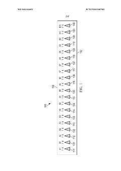
On-chip integrable ordered and highly spectrally uniform single photon sources for scalable quantum optical circuits
PatentWO2024172821A3
Innovation
- Development of mesa-top single quantum dots as a new class of epitaxial quantum dots that provide spatially ordered and spectrally uniform single photon sources for on-chip quantum optical circuits.
- Large-scale on-chip integration of mesa-top single quantum dots with photon manipulating units, enabling entangled photon generation at unprecedented scales (>100-1000 photons).
- Implementation of both monolithic and hybrid integration approaches with silicon photonics to achieve high repetition rates (~>10GHz) for quantum optical circuits.

System and method for optical input/output arrays
PatentWO2016034053A1
Innovation
- Doubling the density of optical I/O arrays in a given footprint on a photonic integrated circuit (PIC) chip through alternating arrangement of first and second optical I/O elements in a row.
- Implementation of partition waveguide routing topology that provides signal feedback to facilitate automated active alignment and coupling of optical fiber arrays to surface grating coupler elements.
- Elimination of waveguide crossings in the routing design while maintaining connectivity between devices and I/O ports, reducing optical losses and crosstalk.
Fabrication Processes and Materials for Photonic Coherent Systems
The fabrication of photonic coherent systems for on-chip applications requires sophisticated processes and specialized materials to ensure precise control of light propagation and coherence management. Silicon photonics has emerged as the dominant platform due to its compatibility with CMOS fabrication techniques, enabling high-volume production and integration with electronic components.
Advanced lithography techniques, particularly deep ultraviolet (DUV) and electron-beam lithography, are essential for creating nanoscale waveguides and resonators with the sub-wavelength precision required for coherent photonic systems. These techniques achieve feature sizes down to 20nm, critical for controlling phase relationships in large-scale arrays.
Material selection significantly impacts coherence management capabilities. Silicon-on-insulator (SOI) remains the industry standard, offering low propagation losses (0.1-0.5 dB/cm) and strong light confinement. However, emerging materials such as silicon nitride (Si3N4) provide superior performance for coherent applications due to lower nonlinear effects and broader transparency windows, albeit with more complex fabrication requirements.
Deposition techniques for these materials have evolved substantially, with plasma-enhanced chemical vapor deposition (PECVD) and low-pressure chemical vapor deposition (LPCVD) enabling precise control of film thickness and composition. These parameters directly affect the effective refractive index and consequently the coherence properties of integrated photonic circuits.
Etching processes represent another critical fabrication step, with reactive ion etching (RIE) and inductively coupled plasma (ICP) etching providing the anisotropic profiles necessary for low-loss waveguides. The sidewall roughness must be minimized to reduce scattering losses that would otherwise degrade coherence in large-scale arrays.
Post-fabrication treatments, including thermal annealing and chemical-mechanical polishing, have proven essential for reducing material defects and surface roughness that contribute to phase noise and coherence degradation. These processes can improve propagation losses by up to 30%, significantly enhancing the scalability of coherent photonic systems.
Recent innovations in heterogeneous integration techniques have enabled the incorporation of III-V materials like indium phosphide with silicon photonics, allowing on-chip integration of active components such as lasers and amplifiers. This capability is transformative for coherent systems, as it addresses the challenge of maintaining coherence across multiple light sources within large-scale arrays.
The development of wafer-scale testing methodologies specific to coherent photonic systems has accelerated manufacturing yields, with automated optical characterization systems capable of mapping phase relationships across thousands of components simultaneously.
Energy Efficiency Considerations in Large-Scale Photonic Integration
Energy efficiency has emerged as a critical consideration in the development of large-scale photonic integrated circuits, particularly for coherence management in on-chip photonic arrays. As photonic systems scale up to accommodate more complex functionalities, power consumption becomes a limiting factor that can significantly impact overall system performance and operational costs.
Traditional electronic interconnects suffer from resistive losses that increase with data rates, whereas photonic interconnects offer inherently lower energy consumption for high-bandwidth data transmission. However, coherence management in large-scale photonic arrays presents unique energy challenges that must be addressed through innovative design approaches.
The energy consumption in photonic coherence management can be categorized into several components: laser source power, modulation energy, coherence maintenance circuitry, and thermal management. Laser sources typically represent the largest energy consumer, with efficiency rates often below 20% for on-chip integration. Recent advances in silicon-compatible III-V lasers have demonstrated improved wall-plug efficiencies approaching 30%, but further improvements are necessary for truly energy-efficient large-scale systems.
Modulation energy represents another significant consideration, with current solutions requiring approximately 10-50 fJ/bit for high-speed operation. Coherent systems typically demand more sophisticated modulation schemes, increasing this energy footprint. Research into electro-optic materials with enhanced Pockels coefficients shows promise for reducing modulation energy requirements by an order of magnitude.
Thermal management presents particular challenges for coherence maintenance, as phase relationships in photonic circuits are highly temperature-sensitive. Active thermal stabilization can consume substantial power, sometimes exceeding the optical power budget itself. Passive athermal designs utilizing materials with compensating thermo-optic coefficients offer a potential solution, though integration complexity increases.
Novel approaches to energy-efficient coherence management include adiabatic wavelength conversion, which can maintain coherence while shifting between optimal wavelengths for different operations. Additionally, recent demonstrations of coherent optical computing architectures suggest that maintaining coherence throughout computational processes can actually reduce overall energy consumption by eliminating optical-electronic-optical conversion steps.
Looking forward, heterogeneous integration of specialized materials optimized for specific functions presents the most promising path toward energy-efficient large-scale photonic systems with robust coherence management capabilities. This approach allows designers to leverage the ideal properties of different material platforms while minimizing the energy penalties associated with maintaining system-wide coherence.
Unlock deeper insights with Patsnap Eureka Quick Research — get a full tech report to explore trends and direct your research. Try now!
Generate Your Research Report Instantly with AI Agent
Supercharge your innovation with Patsnap Eureka AI Agent Platform!