Packaging And Test Strategies For Photonic Neural Modules
AUG 29, 202510 MIN READ
Generate Your Research Report Instantly with AI Agent
Patsnap Eureka helps you evaluate technical feasibility & market potential.
Photonic Neural Module Packaging Background and Objectives
Photonic neural networks represent a revolutionary approach to computing that leverages light instead of electricity to process information, offering potential advantages in speed, energy efficiency, and bandwidth. The development of these systems has evolved significantly over the past decade, transitioning from theoretical concepts to practical implementations that demonstrate increasing levels of integration and functionality. The convergence of photonics and neural computing addresses critical limitations in traditional electronic neural networks, particularly in terms of power consumption and processing speed for large-scale AI applications.
The packaging of photonic neural modules presents unique challenges compared to conventional electronic integrated circuits. Historically, photonic components required bulky optical tables with precise alignment mechanisms, making them impractical for commercial deployment. Recent advances in silicon photonics, III-V integration, and heterogeneous packaging technologies have enabled more compact and robust implementations, though significant challenges remain in achieving the reliability and cost-effectiveness needed for widespread adoption.
Current technological trajectories indicate a move toward higher levels of integration, with efforts focused on combining multiple photonic neural network components—including light sources, modulators, waveguides, detectors, and control electronics—into cohesive, manufacturable modules. This integration trend follows similar patterns observed in electronic integrated circuits but must address the additional complexities of optical alignment, thermal management, and coupling efficiency.
The primary objectives for photonic neural module packaging development include achieving higher integration density while maintaining optical performance, ensuring thermal stability across operating conditions, developing standardized interfaces for modular scaling, and establishing reliable manufacturing processes that can transition from laboratory demonstrations to volume production. These objectives must be pursued while simultaneously reducing costs to compete with established electronic solutions.
Market drivers for this technology include the exponential growth in AI computational demands, increasing power constraints in data centers, and the need for specialized accelerators for specific neural network architectures. The development of effective packaging and test strategies is critical to bridging the gap between promising laboratory demonstrations and commercially viable products that can address these market needs.
Technical benchmarks for successful photonic neural module packaging include insertion loss below critical thresholds, thermal stability across operating temperature ranges, mechanical robustness against environmental stresses, and manufacturing yield rates compatible with commercial production. Meeting these benchmarks requires interdisciplinary expertise spanning photonic design, materials science, thermal engineering, and precision manufacturing.
Market Analysis for Integrated Photonic Neural Networks
The integrated photonic neural network market is experiencing rapid growth, driven by increasing demands for high-speed, energy-efficient computing solutions for artificial intelligence applications. Current market valuations indicate the global photonic integrated circuit market reached approximately $1.3 billion in 2022, with photonic neural network applications representing an emerging segment expected to grow at a CAGR of 25-30% through 2030.
Key market drivers include the exponential increase in data processing requirements for AI workloads, growing limitations of electronic computing architectures, and the need for reduced power consumption in data centers. Photonic neural networks offer significant advantages in these areas, potentially delivering 100-1000x improvements in energy efficiency compared to electronic counterparts while providing superior processing speeds for specific AI operations.
Market segmentation reveals several distinct application sectors. The data center market represents the largest immediate opportunity, where photonic neural modules can accelerate machine learning inference tasks while reducing operational costs. Telecommunications forms another significant segment, where photonic neural networks can enhance signal processing and network optimization. Edge computing applications are emerging rapidly, particularly in autonomous vehicles, industrial automation, and smart infrastructure, where real-time processing with minimal latency is critical.
Geographically, North America currently dominates market investment, accounting for approximately 45% of global activity, followed by Europe (25%) and Asia-Pacific (20%). China has significantly increased investments in photonic computing technologies as part of its national AI strategy, with government funding exceeding $1 billion for photonics research initiatives.
Customer requirements analysis indicates that packaging and testing solutions must address several market needs: scalability for high-volume production, standardization of interfaces, reliability under varied environmental conditions, and cost-effectiveness. Current market barriers include high manufacturing costs, lack of standardized testing protocols, and integration challenges with existing electronic systems.
The competitive landscape features both established semiconductor companies expanding into photonics and specialized startups. Major players include Intel, IBM, and NTT with significant patent portfolios, alongside emerging companies like Lightmatter, Lightelligence, and Luminous Computing that have collectively raised over $300 million in venture funding since 2018.
Market forecasts suggest that as packaging and testing solutions mature, the integrated photonic neural network market could reach $5-7 billion by 2030, with applications expanding beyond current use cases into medical diagnostics, financial modeling, and advanced scientific computing.
Current Challenges in Photonic Neural Module Packaging
Photonic neural modules face significant packaging challenges that impede their widespread commercial adoption. The integration of optical and electronic components within a single package presents complex thermal management issues. During operation, lasers and modulators generate substantial heat that must be efficiently dissipated to maintain performance stability and prevent wavelength drift. Current cooling solutions often add considerable bulk to the overall package, limiting miniaturization efforts essential for practical deployment.
Alignment precision represents another critical challenge, as photonic components typically require sub-micron positioning accuracy. Even minor misalignments between waveguides, detectors, and light sources can cause substantial coupling losses, degrading overall system performance. Traditional packaging methods struggle to maintain this precision across varying environmental conditions and over the device lifetime, particularly when thermal cycling occurs during normal operation.
Material compatibility issues further complicate packaging strategies. The diverse materials used in photonic neural modules—including silicon, III-V semiconductors, polymers, and various metals—exhibit different coefficients of thermal expansion. These disparities create mechanical stress during temperature fluctuations, potentially causing component failure or performance degradation over time. Additionally, hermetic sealing requirements to protect sensitive optical surfaces from environmental contaminants add another layer of complexity.
Testing methodologies for packaged photonic neural modules remain underdeveloped compared to electronic counterparts. The industry lacks standardized testing protocols that can efficiently evaluate optical performance parameters alongside electronic functionality. Current testing approaches often require custom setups that are time-consuming and difficult to scale for high-volume manufacturing, creating a significant bottleneck in production pipelines.
Manufacturability concerns persist as many packaging solutions developed in laboratory settings prove challenging to transfer to high-volume production environments. Techniques that work well for prototype development frequently lack the repeatability and yield rates necessary for commercial viability. The absence of automated assembly processes specifically designed for photonic neural modules further exacerbates this issue.
Cost considerations represent perhaps the most pressing challenge. Current packaging approaches can account for up to 80% of the total device cost, making photonic neural modules prohibitively expensive for many potential applications. This cost barrier stems from specialized materials, precision equipment requirements, and labor-intensive assembly processes that have not benefited from the economies of scale seen in conventional electronics manufacturing.
Reliability testing frameworks remain inadequate for predicting the long-term performance of packaged photonic neural modules in real-world deployment scenarios. Accelerated aging tests that accurately model the complex degradation mechanisms affecting both optical and electronic components are still being developed, creating uncertainty around device lifetimes and maintenance requirements.
Current Packaging and Test Solutions for Photonic Modules
01 Integration and packaging techniques for photonic neural modules
Advanced packaging techniques are essential for integrating photonic neural modules with electronic components. These techniques include flip-chip bonding, wafer-level packaging, and 3D integration methods that enable efficient coupling between optical and electronic elements. The packaging solutions must address thermal management challenges while maintaining precise alignment of optical components to ensure signal integrity across the neural network architecture.- Optical Interconnect Packaging Solutions: Advanced packaging techniques for integrating photonic components with neural network modules. These solutions focus on efficient light coupling between optical elements and electronic circuits, including waveguide integration, fiber alignment mechanisms, and hermetic sealing methods to protect sensitive photonic elements. The packaging designs optimize signal integrity while minimizing optical losses at interfaces between different materials and components.
- Testing Methodologies for Photonic Neural Networks: Specialized testing approaches for evaluating the performance and reliability of photonic neural modules. These methodologies include optical signal integrity verification, wavelength accuracy testing, thermal stability assessment, and accelerated aging tests. The testing strategies address unique challenges of photonic neural networks such as optical crosstalk, wavelength drift, and coupling efficiency degradation over time.
- Integration of Photonic and Electronic Components: Techniques for hybrid integration of photonic elements with electronic neural processing units. These approaches include co-packaging strategies for photonic integrated circuits with electronic chips, thermal management solutions for dissipating heat from both optical and electronic components, and interface designs that optimize signal conversion between optical and electrical domains. The integration methods aim to minimize latency while maximizing computational efficiency.
- Scalable Manufacturing Processes for Photonic Neural Modules: Manufacturing techniques that enable cost-effective production of photonic neural network components at scale. These processes include automated assembly methods for precise alignment of optical components, wafer-level testing procedures, and standardized packaging platforms that support high-volume production. The manufacturing approaches focus on yield improvement, process repeatability, and compatibility with existing semiconductor fabrication infrastructure.
- Performance Optimization and Calibration Systems: Methods and systems for calibrating and optimizing the performance of photonic neural modules after packaging. These include in-situ monitoring techniques for real-time performance assessment, adaptive calibration algorithms that compensate for manufacturing variations, and feedback systems that adjust optical parameters to maintain optimal operation under varying environmental conditions. The optimization approaches ensure consistent neural network performance despite component aging and environmental fluctuations.
02 Testing methodologies for photonic neural networks
Specialized testing methodologies have been developed for evaluating the performance of photonic neural modules. These include optical signal integrity testing, waveguide characterization, and neural network functionality verification. Test strategies incorporate both component-level testing of individual photonic elements and system-level evaluation of the complete neural network, with automated test equipment designed specifically for optical neural computing architectures.Expand Specific Solutions03 Thermal management solutions for photonic neural modules
Thermal management is critical for maintaining the stability and performance of photonic neural modules. Solutions include integrated cooling channels, thermally conductive materials, and active temperature control systems. These approaches help mitigate thermal crosstalk between optical components and electronic elements, ensuring consistent operation of temperature-sensitive photonic devices such as lasers and modulators used in neural network implementations.Expand Specific Solutions04 Optical coupling and alignment strategies
Precise optical coupling and alignment are fundamental to photonic neural module performance. Various strategies have been developed, including self-aligning optical interfaces, precision assembly techniques, and active alignment systems. These approaches ensure efficient light transfer between components such as lasers, waveguides, and photodetectors, minimizing coupling losses and maintaining signal integrity throughout the neural network architecture.Expand Specific Solutions05 Reliability and qualification testing for photonic neural systems
Comprehensive reliability and qualification testing frameworks have been established for photonic neural systems. These include accelerated aging tests, environmental stress screening, and long-term performance monitoring. Testing protocols address specific failure modes of photonic components such as laser degradation, waveguide deterioration, and coupling efficiency changes over time, ensuring the durability and stability of neural network implementations in various operating conditions.Expand Specific Solutions
Leading Companies in Photonic Neural Network Industry
The photonic neural module packaging and test market is in its early growth phase, characterized by increasing demand driven by AI applications requiring higher processing speeds and energy efficiency. The market is projected to expand significantly as silicon photonics technology matures, with current estimates suggesting a compound annual growth rate exceeding 20%. Leading semiconductor giants like Samsung Electronics, TSMC, and Huawei are making substantial investments, while specialized players such as Rockley Photonics and SiPhox are developing innovative integration solutions. Research institutions including MIT, Industrial Technology Research Institute, and Institute of Microelectronics of Chinese Academy of Sciences are advancing fundamental technologies, creating a competitive landscape where collaboration between industry and academia is accelerating commercialization efforts.
Industrial Technology Research Institute
Technical Solution: The Industrial Technology Research Institute (ITRI) has developed a comprehensive packaging and test strategy for photonic neural modules called Photonic Neural Integration Platform (PNIP). Their approach focuses on heterogeneous integration of III-V lasers, silicon photonic circuits, and CMOS electronics using advanced wafer bonding techniques. ITRI's packaging solution employs a novel optical interposer technology that provides passive alignment features, reducing assembly costs while maintaining coupling efficiencies above 85%. Their photonic neural modules incorporate specialized optical fan-out structures that enable efficient distribution of optical signals across multiple neural processing units. ITRI has pioneered a hierarchical testing methodology that begins with component-level characterization and progresses through subsystem verification to full system validation, with automated test equipment capable of simultaneously evaluating optical, electrical, and thermal performance parameters. Their packaging design also addresses reliability concerns through hermetic sealing techniques and specialized stress-relief structures that minimize thermal expansion mismatches between different materials in the package.
Strengths: Cost-effective integration approach suitable for volume production; comprehensive testing methodology ensures high reliability and performance consistency. Weaknesses: Optical interposer technology still maturing compared to electronic interposers; packaging approach optimized for specific applications may limit flexibility.
Taiwan Semiconductor Manufacturing Co., Ltd.
Technical Solution: TSMC has developed an advanced packaging platform specifically for photonic neural modules called Integrated Photonic System-in-Package (IPSiP). This technology leverages TSMC's expertise in advanced semiconductor manufacturing to create highly integrated photonic neural processing units. Their approach combines silicon photonics with conventional CMOS electronics using their CoWoS (Chip-on-Wafer-on-Substrate) packaging technology, enabling high-bandwidth, low-latency connections between photonic and electronic components. TSMC's packaging strategy incorporates precision optical alignment techniques that maintain sub-micron positioning accuracy between optical components, critical for maintaining signal integrity in photonic neural networks. Their testing methodology includes automated wafer-level optical testing that can characterize thousands of photonic components simultaneously, dramatically reducing test time and cost. TSMC has also developed specialized thermal management solutions that address the unique challenges of photonic neural modules, including gradient-based cooling systems that maintain uniform temperatures across photonic elements to prevent wavelength drift in optical signals.
Strengths: Industry-leading manufacturing precision and quality control; established supply chain and production infrastructure enables rapid scaling. Weaknesses: Standardized approach may limit customization options for specialized neural network architectures; high initial investment requirements for new photonic neural module designs.
Key Innovations in Photonic-Electronic Integration
Photonic neural network
PatentActiveUS12340301B2
Innovation
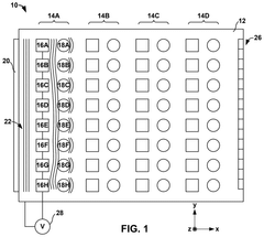
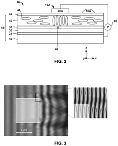
- A photonic neural network device featuring a planar waveguide, a layer with a changeable refractive index, and programmable electrodes that apply configurable voltages to induce amplitude or phase modulation of light, enabling reconfigurable and scalable neural network architecture.
Photonics packaging method and device
PatentActiveUS20200116930A1
Innovation
- A photonic package design with a material layer interposed between the ASIC and the photonic chip, featuring recesses that align with the MEMS devices to form enclosed cavities, preventing extraneous material intrusion and allowing free motion of the devices, while conductive pillars ensure electrical connectivity.
Thermal Management Strategies for Photonic Neural Networks
Thermal management represents a critical challenge in the development and deployment of photonic neural networks (PNNs). As these systems integrate both electronic and photonic components in increasingly dense configurations, heat dissipation becomes a significant limiting factor affecting performance, reliability, and longevity. The thermal characteristics of photonic neural modules differ substantially from traditional electronic systems due to the unique properties of optical components and their sensitivity to temperature variations.
Current thermal management approaches for PNNs can be categorized into passive and active cooling strategies. Passive techniques include specialized heat spreaders, thermal interface materials (TIMs), and advanced packaging designs that optimize heat flow paths. These solutions typically employ materials with high thermal conductivity such as diamond-based composites, graphene, and specialized metal alloys that can efficiently transfer heat away from critical components without requiring additional power input.
Active cooling methods encompass thermoelectric coolers (TECs), microfluidic cooling channels, and phase-change cooling systems. TECs offer precise temperature control but add power consumption overhead. Microfluidic cooling solutions, while more complex to implement, provide superior cooling efficiency by circulating coolants directly through or adjacent to heat-generating components. These systems can achieve thermal gradients below 0.1°C across the photonic chip surface, which is essential for maintaining consistent optical properties.
Temperature-dependent wavelength drift in photonic components presents a particular challenge, as even minor thermal fluctuations can significantly impact system performance. Research indicates that silicon photonic waveguides typically exhibit wavelength shifts of approximately 70-80 pm/°C, necessitating either robust temperature stabilization or adaptive compensation mechanisms. Advanced thermal management solutions now incorporate real-time temperature monitoring and feedback systems that dynamically adjust operating parameters to maintain optimal performance despite thermal variations.
Heterogeneous integration of electronic and photonic components compounds thermal management challenges due to differing thermal expansion coefficients and optimal operating temperature ranges. Novel approaches include thermally isolated packaging designs that decouple temperature-sensitive photonic elements from heat-generating electronic components. These designs often utilize specialized thermal breaks, selective heat channeling, and strategically positioned cooling elements to create distinct thermal zones within a single package.
Emerging research focuses on bio-inspired cooling solutions that mimic natural heat dissipation systems, such as vascular networks and transpiration cooling. These approaches promise more efficient and uniform cooling with reduced power requirements. Additionally, machine learning algorithms are increasingly being employed to predict thermal behavior and optimize cooling strategies in real-time, adapting to changing workloads and environmental conditions to maintain optimal thermal performance while minimizing energy consumption.
Standardization Efforts in Photonic Neural Module Testing
The standardization of testing methodologies for photonic neural modules represents a critical frontier in ensuring industry-wide compatibility, reliability, and performance benchmarking. Currently, several international organizations are spearheading efforts to establish comprehensive testing frameworks specifically tailored for photonic neural computing systems.
The IEEE P3109 Working Group has been particularly active in developing standards for neuromorphic computing devices, with a dedicated subcommittee focusing on photonic implementations. Their draft standard addresses critical parameters including optical power stability, wavelength accuracy, and coherence properties that are unique to photonic neural networks.
The International Electrotechnical Commission (IEC) has established Technical Committee 113, which is working on standardized test procedures for integrated photonic devices. Their recent publication IEC 62951-7 outlines testing protocols for photonic-electronic hybrid systems, providing valuable guidance for neural module validation.
Industry consortia are also making significant contributions to standardization efforts. The Consortium for Photonic Neural Computing (CPNC), comprising leading technology companies and research institutions, has published a comprehensive testing framework that addresses both component-level and system-level performance metrics. Their "Photonic Neural Module Testing Specification v1.2" has gained traction as a de facto industry standard.
Testing standardization efforts are focusing on several key areas. First, optical signal integrity testing protocols are being developed to ensure consistent signal quality across different photonic neural implementations. Second, standardized benchmarking suites are emerging to enable fair comparison of different photonic neural architectures. These include both synthetic test patterns and real-world neural network workloads.
Thermal stability testing represents another critical area of standardization, as temperature fluctuations can significantly impact the performance of photonic components. The emerging standards specify precise temperature control requirements and testing methodologies to ensure consistent operation across varying environmental conditions.
Interoperability testing frameworks are also being established to ensure that photonic neural modules from different manufacturers can work together seamlessly. This includes standardized interfaces for both optical and electronic connections, as well as data exchange protocols.
The convergence toward unified testing standards is accelerating industry adoption of photonic neural technologies by reducing integration risks and enabling more accurate performance comparisons. However, challenges remain in harmonizing competing standards and addressing the rapid pace of technological innovation in this field.
Unlock deeper insights with Patsnap Eureka Quick Research — get a full tech report to explore trends and direct your research. Try now!
Generate Your Research Report Instantly with AI Agent
Supercharge your innovation with Patsnap Eureka AI Agent Platform!