Noise And Crosstalk Mitigation In Dense Photonic Neuromorphic Chips
AUG 29, 20259 MIN READ
Generate Your Research Report Instantly with AI Agent
Patsnap Eureka helps you evaluate technical feasibility & market potential.
Photonic Neuromorphic Computing Background and Objectives
Photonic neuromorphic computing represents a revolutionary paradigm in computational architecture that merges the principles of neuromorphic engineering with integrated photonics. This approach aims to emulate the brain's neural networks using light rather than electricity, offering unprecedented advantages in processing speed, energy efficiency, and bandwidth. The evolution of this technology can be traced back to the early 2000s when researchers began exploring optical implementations of neural networks, but significant advancements have accelerated in the past decade with the maturation of silicon photonics and nanofabrication techniques.
The fundamental principle behind photonic neuromorphic computing lies in leveraging optical phenomena such as interference, diffraction, and nonlinear effects to perform neural network operations. Unlike electronic systems constrained by resistance and capacitance, photonic systems operate at the speed of light with minimal heat generation, potentially enabling processing speeds orders of magnitude faster than conventional electronic neural networks.
Recent technological milestones include the development of photonic tensor cores, integrated optical frequency combs for parallel processing, and phase-change materials for persistent photonic memory. These innovations have collectively pushed the field toward practical implementations of optical neural networks capable of handling complex machine learning tasks.
The current trajectory of photonic neuromorphic computing is driven by several key trends: miniaturization of photonic components, heterogeneous integration with electronic systems, development of specialized optical materials, and novel architectures optimized for specific computational tasks. The convergence of these trends is creating a fertile ground for addressing the increasing computational demands of artificial intelligence and machine learning applications.
The primary objective in addressing noise and crosstalk mitigation in dense photonic neuromorphic chips is to enhance the signal integrity and computational fidelity of these systems. As photonic neural networks scale to higher densities, unwanted interactions between closely packed waveguides and optical components introduce noise and crosstalk that degrade performance and limit scalability. Resolving these challenges is critical for realizing the full potential of photonic neuromorphic computing in practical applications.
Additional technical goals include developing robust isolation techniques between adjacent photonic components, creating adaptive compensation mechanisms for environmental variations, establishing standardized metrics for signal integrity in photonic neural networks, and designing scalable architectures that maintain computational accuracy despite increasing integration density. Success in these objectives would significantly advance the field toward commercially viable photonic neuromorphic systems capable of outperforming electronic counterparts in specific computational domains.
Market Analysis for Dense Photonic Neural Networks
The global market for photonic neural networks is experiencing significant growth, driven by increasing demands for high-speed, energy-efficient computing solutions. Current market valuations indicate that the neuromorphic computing sector is projected to reach 8.9 billion USD by 2025, with photonic implementations capturing an expanding share due to their superior performance characteristics in specific applications.
Dense photonic neural networks represent a particularly promising segment within this market, offering unprecedented computational capabilities for complex AI tasks. These systems leverage light-based processing to achieve parallel computation at speeds significantly exceeding electronic counterparts, while consuming substantially less power. Market research indicates that data centers and high-performance computing facilities are showing strong interest in this technology, primarily motivated by potential energy savings of up to 90% compared to traditional electronic systems.
The telecommunications sector presents another substantial market opportunity, with major carriers seeking solutions to handle exponentially growing data traffic while minimizing energy consumption. Photonic neural networks offer compelling advantages for signal processing, pattern recognition, and optimization problems that are prevalent in network management and security applications.
Healthcare and biomedical research constitute emerging markets with significant potential, particularly for applications requiring real-time processing of complex imaging data. The ability of dense photonic neural networks to process multidimensional data in parallel makes them ideal for advanced medical imaging analysis, potentially reducing diagnostic times from hours to seconds.
Financial services represent another key market segment, with institutions increasingly adopting AI for fraud detection, algorithmic trading, and risk assessment. The ultra-low latency capabilities of photonic neural networks provide a competitive advantage in time-sensitive financial applications where microseconds can translate to substantial monetary differences.
Market adoption faces several challenges, including high initial implementation costs and integration complexities with existing electronic infrastructure. However, the total cost of ownership analysis increasingly favors photonic solutions when considering operational energy savings over system lifetimes.
Regional analysis shows North America leading in research and early adoption, with approximately 45% of current market activity. Asia-Pacific represents the fastest-growing region, driven by substantial investments in China, Japan, and South Korea. European markets show strong interest, particularly in research applications and specialized industrial implementations.
The competitive landscape remains dynamic, with both established semiconductor companies and specialized photonics startups vying for market position. Strategic partnerships between hardware manufacturers, software developers, and end-users are becoming increasingly common as the ecosystem matures and standardization efforts progress.
Noise and Crosstalk Challenges in Integrated Photonics
Integrated photonic systems face significant challenges related to noise and crosstalk, particularly as device density increases in neuromorphic computing applications. These issues stem from fundamental physical limitations and become more pronounced as components are packed closer together on photonic chips. The primary noise sources include thermal noise from temperature fluctuations, shot noise from quantum uncertainties in photon detection, and amplifier noise in optical-electrical conversion processes.
Crosstalk, the unintended coupling of signals between adjacent waveguides or components, represents a major obstacle in dense photonic integration. This phenomenon occurs through several mechanisms: evanescent coupling where optical modes extend beyond waveguide boundaries, substrate coupling through shared silicon substrates, and reflection-induced crosstalk at waveguide junctions and interfaces. These effects significantly degrade signal integrity and limit the achievable density of photonic neural networks.
The severity of these challenges scales non-linearly with integration density. As waveguides are placed closer together to increase computational density, crosstalk increases exponentially rather than linearly. This creates a fundamental trade-off between integration density and signal fidelity that must be carefully managed in photonic neuromorphic chip design.
Temperature sensitivity compounds these issues, as thermal gradients across a chip can cause wavelength drift and change coupling coefficients between components. This is particularly problematic for wavelength division multiplexing (WDM) systems where precise wavelength control is essential. Even small temperature variations of 1-2°C can shift resonances enough to cause significant performance degradation.
Manufacturing variations introduce additional complexity, as fabrication tolerances lead to dimensional inconsistencies that affect waveguide properties and coupling characteristics. These variations are typically on the scale of nanometers but can substantially impact optical performance, especially in high-precision applications like neuromorphic computing where weight accuracy is crucial.
The combined effect of these challenges creates a complex design space where traditional electronic design approaches are insufficient. Unlike electronic circuits where signals are largely confined to conductors, optical signals interact through free-space coupling and interference effects that require sophisticated electromagnetic modeling. This fundamentally changes the design paradigm for integrated photonics compared to electronic integrated circuits.
Current state-of-the-art photonic neuromorphic chips typically achieve integration densities of 100-1000 neurons per square centimeter, orders of magnitude lower than their electronic counterparts, largely due to these noise and crosstalk limitations. Overcoming these challenges is essential for photonic neuromorphic computing to compete with electronic implementations in terms of scale and energy efficiency.
Current Noise Mitigation Techniques in Photonic Chips
01 Noise reduction techniques in photonic neuromorphic chips
Various techniques can be employed to reduce noise in photonic neuromorphic chips, enhancing their performance and reliability. These include specialized signal processing algorithms, optical filtering methods, and advanced circuit designs that minimize thermal noise and interference. By implementing these noise reduction strategies, the signal-to-noise ratio can be improved, leading to more accurate neural computations and better overall system performance.- Noise reduction techniques in photonic neuromorphic chips: Various techniques can be employed to reduce noise in photonic neuromorphic chips, enhancing their performance and reliability. These include specialized circuit designs, filtering mechanisms, and signal processing algorithms that minimize unwanted signal fluctuations. By implementing these noise reduction strategies, the signal-to-noise ratio can be improved, leading to more accurate neural computations and better overall system performance in neuromorphic computing applications.
- Crosstalk mitigation in optical neural networks: Crosstalk between optical waveguides and components is a significant challenge in photonic neuromorphic chips. Mitigation strategies include optimized waveguide design, isolation techniques, and specialized component layouts that minimize unwanted interactions between adjacent optical paths. Advanced materials and fabrication techniques can also be employed to reduce optical interference, ensuring that signals propagate through the network with minimal distortion from neighboring channels.
- Integration of monitoring and feedback systems: Implementing real-time monitoring and feedback systems in photonic neuromorphic chips allows for dynamic adjustment to compensate for noise and crosstalk issues. These systems can detect performance degradation, identify sources of interference, and automatically apply corrective measures. Adaptive algorithms can continuously optimize chip operation by adjusting optical power levels, timing parameters, and signal routing to maintain optimal performance despite environmental changes or component aging.
- Novel architectural designs for signal integrity: Innovative architectural approaches can fundamentally improve signal integrity in photonic neuromorphic systems. These include hierarchical network structures, redundant pathways, and specialized node designs that inherently resist noise and crosstalk effects. Some architectures incorporate isolation zones, buffer regions, or dedicated calibration circuits that maintain clean signal transmission throughout the neural network, even as complexity and integration density increase.
- Simulation and modeling tools for noise prediction: Advanced simulation and modeling tools are essential for predicting and addressing noise and crosstalk issues before physical implementation. These computational approaches can model complex electromagnetic interactions, thermal effects, and quantum noise sources within photonic neural networks. By accurately simulating system behavior under various operating conditions, designers can identify potential problems early in the development process and implement appropriate countermeasures, reducing development time and improving final performance.
02 Crosstalk mitigation in optical neural networks
Crosstalk between optical waveguides and components is a significant challenge in photonic neuromorphic chips. Mitigation strategies include optimized waveguide geometries, isolation structures, and specialized materials that reduce optical interference. Advanced layout techniques and proper spacing between optical components can also minimize unwanted interactions between signals, ensuring accurate information processing in densely integrated photonic neural networks.Expand Specific Solutions03 Integration of noise-tolerant architectures
Photonic neuromorphic chips can be designed with inherently noise-tolerant architectures that maintain computational accuracy despite the presence of noise and crosstalk. These architectures may incorporate redundancy, error correction mechanisms, and robust encoding schemes. By designing neural networks that can function effectively in noisy environments, the overall reliability and performance of photonic neuromorphic systems can be significantly improved.Expand Specific Solutions04 Advanced materials and fabrication for noise reduction
The choice of materials and fabrication techniques plays a crucial role in minimizing noise and crosstalk in photonic neuromorphic chips. Low-loss optical materials, precision fabrication methods, and specialized coatings can reduce scattering and absorption losses. Novel materials with enhanced optical properties can improve signal integrity and reduce thermal noise, leading to better performance in neuromorphic computing applications.Expand Specific Solutions05 Simulation and modeling of noise effects
Accurate simulation and modeling tools are essential for understanding and mitigating noise and crosstalk in photonic neuromorphic chips. These tools can predict how noise propagates through the system, identify critical points of interference, and evaluate the effectiveness of various mitigation strategies. By simulating noise effects before fabrication, designers can optimize chip layouts and implement appropriate countermeasures to ensure optimal performance.Expand Specific Solutions
Leading Companies in Photonic Neuromorphic Computing
The photonic neuromorphic chip market is in its early growth phase, characterized by significant research and development efforts addressing noise and crosstalk challenges in dense architectures. While the market size remains relatively modest, it's projected to expand rapidly as neuromorphic computing gains traction in AI applications. Technologically, companies like Samsung Electronics, Taiwan Semiconductor, and Huawei are leading hardware development, while research institutions such as Huazhong University of Science & Technology and Beijing Institute of Technology contribute fundamental innovations. Canon, Micron Technology, and Analog Devices are advancing specialized components addressing signal integrity. The technology remains in pre-maturity stage with significant challenges in scaling dense photonic integration while maintaining signal fidelity, though recent breakthroughs in noise mitigation techniques show promising progress.
Analog Devices, Inc.
Technical Solution: Analog Devices has developed a sophisticated mixed-signal approach to noise and crosstalk mitigation in photonic neuromorphic chips. Their solution integrates specialized analog front-end circuits with photonic elements to provide real-time noise suppression and signal conditioning. ADI's technology employs proprietary optical-electronic feedback loops that continuously monitor and adjust optical signals to maintain optimal signal-to-noise ratios. Their photonic neuromorphic architecture incorporates advanced modulation schemes that are inherently resistant to common noise sources in dense photonic environments. Additionally, ADI has implemented novel optical isolation structures using their expertise in materials engineering, creating effective barriers against optical crosstalk while maintaining compact dimensions suitable for high-density integration. Their solution also features adaptive equalization techniques that compensate for manufacturing variations and aging effects in photonic components.
Strengths: Industry-leading expertise in analog signal processing; seamless integration of electronic and photonic domains; robust performance across varying environmental conditions. Weaknesses: Higher complexity in control systems; increased power requirements for active noise compensation circuits.
Hitachi Ltd.
Technical Solution: Hitachi has developed an innovative approach to noise and crosstalk mitigation in dense photonic neuromorphic chips through their Advanced Photonic Isolation Technology (APIT). This comprehensive solution addresses both optical and thermal crosstalk through a multi-layered strategy. At the physical layer, Hitachi employs proprietary waveguide designs with specialized cladding materials that create highly effective optical barriers between adjacent photonic neurons. Their technology incorporates nanoscale optical isolators that can be integrated directly into the photonic circuit, providing localized protection against signal interference. Hitachi has also developed sophisticated signal processing algorithms that can distinguish between intended signals and noise, enabling effective digital compensation for residual crosstalk effects. Additionally, their thermal management system uses strategically placed heat sinks and thermal isolation trenches to minimize temperature-induced drift in optical properties.
Strengths: Comprehensive approach addressing both optical and thermal crosstalk; extensive manufacturing capabilities for complex photonic structures; strong integration with existing computing platforms. Weaknesses: Higher fabrication complexity may impact yield rates; solution may require more chip area than some competing approaches.
Key Patents in Photonic Crosstalk Reduction
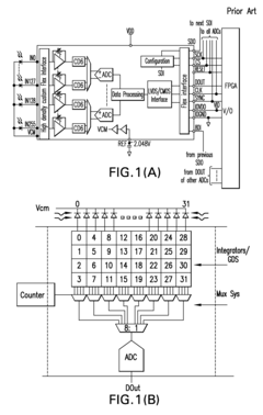
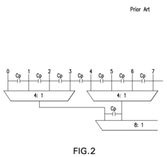
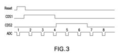
Semiconductor device having a shielding line for signal crosstalk suppression
PatentPendingUS20230268287A1
Innovation
- A semiconductor device with a shielding line is introduced between signal lines, connected to power or ground, to reduce or prevent electromagnetic noise, and the manufacturing process employs pitch multiplication techniques like self-aligned pitch doubling to maintain close line spacing and overcome lithography issues.
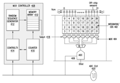
System and method for reducing pattern noise in analog system processing
PatentActiveUS20110043397A1
Innovation
- Randomizing the sampling sequence of ADC converters by using a multiplexer with a pseudo-random index generator and controller to scatter system activities across all data channels, effectively converting correlated pattern noise into uncorrelated noise indistinguishable from system noise.
Thermal Management Strategies for Photonic Neural Networks
Thermal management represents a critical challenge in the development of dense photonic neuromorphic chips, particularly as these systems face increasing integration densities. The operational efficiency of photonic neural networks is highly temperature-dependent, with thermal fluctuations directly impacting signal integrity and contributing to noise and crosstalk issues. Current research indicates that even minor temperature variations of 1-2°C can significantly alter the refractive indices of waveguides, resulting in phase shifts that compromise computational accuracy.
Several thermal management approaches have emerged to address these challenges. Passive cooling strategies utilize specialized materials with high thermal conductivity to efficiently dissipate heat. Silicon carbide and diamond-based substrates have shown promising results, offering thermal conductivity values 3-5 times higher than traditional silicon substrates while maintaining compatibility with existing fabrication processes.
Active cooling technologies represent another frontier, with thermoelectric coolers (TECs) being integrated directly into photonic circuits. These micro-scale cooling elements can provide localized temperature control with precision reaching ±0.1°C, significantly reducing thermal crosstalk between adjacent photonic components. Recent advancements in TEC design have improved energy efficiency by approximately 30% compared to previous generations.
Thermal isolation techniques form a complementary approach, employing trenches and air gaps to minimize heat transfer between critical components. Studies have demonstrated that strategically placed thermal isolation structures can reduce thermal crosstalk by up to 70% in densely packed photonic circuits, though at the cost of increased chip area requirements of 15-20%.
Dynamic thermal compensation represents perhaps the most sophisticated approach, utilizing integrated temperature sensors and feedback control systems. These systems continuously monitor thermal conditions and apply real-time adjustments to operational parameters. Machine learning algorithms have been successfully deployed to predict thermal patterns and preemptively adjust optical properties, reducing thermally-induced errors by up to 85% in experimental systems.
The integration of these thermal management strategies must be considered early in the design phase of photonic neural networks. Simulation tools that accurately model heat distribution have become essential in this process, with recent thermal-optical co-simulation platforms demonstrating prediction accuracies within 5% of experimental measurements. As photonic neuromorphic computing advances toward higher densities and processing capabilities, thermal management will remain a fundamental consideration in mitigating noise and crosstalk challenges.
Benchmarking and Performance Metrics for Photonic Computing
Establishing standardized benchmarks and performance metrics for photonic computing systems is essential for evaluating noise and crosstalk mitigation techniques in dense photonic neuromorphic chips. Current benchmarking approaches often lack consistency, making it difficult to compare different solutions across research groups and industry implementations.
The primary performance metrics for evaluating noise and crosstalk mitigation include signal-to-noise ratio (SNR), bit error rate (BER), and crosstalk isolation. For neuromorphic applications specifically, metrics such as inference accuracy, energy efficiency (measured in femtojoules per operation), and computational density (operations per square millimeter) provide critical insights into the effectiveness of mitigation strategies.
Temperature stability represents another crucial benchmark, as thermal fluctuations significantly impact noise profiles in photonic circuits. Successful mitigation techniques must demonstrate performance consistency across operating temperature ranges of at least -20°C to 85°C for commercial viability. Metrics should include thermal sensitivity coefficients and performance degradation measurements under thermal stress.
Standardized test patterns have emerged to evaluate crosstalk in dense photonic neuromorphic architectures. These include worst-case adjacent channel activation scenarios and randomized workloads that simulate real neural network operations. The MLPerf Inference benchmark suite, adapted for photonic implementations, offers a promising framework for comparative analysis across different hardware platforms.
Latency measurements must account for both optical propagation delays and electronic-photonic conversion overhead. End-to-end system benchmarks should evaluate not only isolated component performance but also full-system metrics under realistic workloads, as noise and crosstalk effects often manifest differently at the system level compared to component-level testing.
Time-domain analysis provides critical insights into dynamic noise characteristics, particularly important for neuromorphic systems where temporal information processing is fundamental. Metrics such as timing jitter, pulse distortion, and inter-symbol interference quantify the temporal fidelity of optical signals in the presence of noise and crosstalk.
Industry consortia including the Photonic Computing Benchmark Alliance (PCBA) and academic initiatives are working to establish standardized benchmark suites specifically designed for photonic neuromorphic systems. These efforts aim to create fair comparison methodologies that account for the unique characteristics of optical computing platforms while enabling meaningful comparisons with electronic counterparts.
Unlock deeper insights with Patsnap Eureka Quick Research — get a full tech report to explore trends and direct your research. Try now!
Generate Your Research Report Instantly with AI Agent
Supercharge your innovation with Patsnap Eureka AI Agent Platform!