Materials Selection For Low-Loss Waveguides In Neuromorphic Chips
AUG 29, 202510 MIN READ
Generate Your Research Report Instantly with AI Agent
Patsnap Eureka helps you evaluate technical feasibility & market potential.
Neuromorphic Photonics Background and Objectives
Neuromorphic photonics represents a revolutionary approach to computing that combines the principles of neuromorphic engineering with integrated photonics. This emerging field aims to emulate the brain's neural architecture using optical components, offering unprecedented advantages in speed, energy efficiency, and computational density. The evolution of neuromorphic photonics can be traced back to the convergence of two distinct research domains: neuromorphic computing, pioneered by Carver Mead in the late 1980s, and integrated photonics, which gained significant momentum in the early 2000s with advances in silicon photonics fabrication techniques.
The fundamental premise of neuromorphic photonics lies in leveraging light's inherent parallelism and high bandwidth to implement neural network functionalities. Unlike electronic neuromorphic systems that face limitations due to resistance-capacitance delays and heat dissipation, photonic implementations can potentially operate at speeds several orders of magnitude faster while consuming significantly less power. This paradigm shift addresses the growing computational demands that conventional electronic architectures struggle to meet.
Recent technological advancements have accelerated interest in this field, particularly the development of efficient optical nonlinear elements, phase-change materials, and novel waveguide structures that enable complex optical signal processing. These innovations have made it increasingly feasible to implement critical neural network operations such as weighted summation, nonlinear activation, and spike generation using purely optical or hybrid opto-electronic approaches.
The primary technical objectives in neuromorphic photonics research center around developing low-loss waveguide materials and structures that can efficiently guide light while enabling the necessary optical interactions for neural computation. Material selection represents a critical challenge, as ideal materials must simultaneously exhibit low propagation losses, strong nonlinear responses, compatibility with existing fabrication processes, and thermal stability. Silicon, silicon nitride, indium phosphide, and various chalcogenide glasses have emerged as promising candidates, each offering distinct advantages for specific applications.
Beyond material considerations, neuromorphic photonic systems aim to achieve several ambitious goals: ultra-high processing speeds exceeding terahertz frequencies, energy efficiencies approaching femtojoules per operation, high integration densities, and robust learning capabilities. These objectives align with the broader vision of creating computing systems that can process complex, real-world data with the efficiency and adaptability characteristic of biological neural networks.
The trajectory of neuromorphic photonics is increasingly influenced by advances in machine learning algorithms, particularly spiking neural networks and reservoir computing, which are naturally suited for photonic implementation. As these computational paradigms continue to evolve, they create new opportunities and requirements for the underlying photonic hardware, driving innovation in waveguide design and material selection.
Market Analysis for Low-Loss Waveguide Technologies
The global market for low-loss waveguide technologies in neuromorphic computing is experiencing significant growth, driven by the increasing demand for energy-efficient computing solutions and the rapid advancement of artificial intelligence applications. Current market estimates value the neuromorphic chip sector at approximately $3.1 billion in 2023, with projections indicating a compound annual growth rate of 24% through 2030.
Low-loss waveguide technologies represent a critical component within this market, as they directly impact the performance, energy efficiency, and scalability of neuromorphic computing systems. The demand for these specialized waveguides is particularly strong in research institutions, semiconductor manufacturers, and technology companies investing in next-generation computing architectures.
Market segmentation reveals distinct application areas driving demand for low-loss waveguides in neuromorphic chips. The largest segment currently comprises research and development activities at universities and corporate laboratories, accounting for approximately 45% of market volume. Commercial applications in data centers and edge computing devices represent the fastest-growing segment, with 32% annual growth as these technologies begin transitioning from research to production environments.
Geographically, North America leads the market with 38% share, followed by Asia-Pacific at 34% and Europe at 22%. China and South Korea are demonstrating the most aggressive growth rates, supported by substantial government investments in semiconductor technologies and artificial intelligence research.
Customer requirements are evolving rapidly, with increasing emphasis on waveguides that can support higher data transmission rates while maintaining minimal signal loss. Industry surveys indicate that 78% of potential adopters consider material selection for low-loss properties as "extremely important" in their purchasing decisions, while 65% prioritize compatibility with existing semiconductor manufacturing processes.
Market barriers include the high cost of specialized materials, technical challenges in achieving consistent manufacturing quality, and the relatively limited supplier ecosystem. The average development cost for new waveguide materials suitable for neuromorphic applications ranges between $5-8 million, creating significant entry barriers for smaller players.
Pricing trends show gradual reduction as manufacturing scales increase, with current premium materials commanding 3-5 times the cost of conventional alternatives. Market analysts predict this premium will decrease to 1.5-2 times by 2027 as production volumes increase and manufacturing processes mature.
The competitive landscape features both established semiconductor materials providers and specialized startups focusing exclusively on photonic and neuromorphic computing materials. Strategic partnerships between material developers and chip manufacturers are becoming increasingly common, creating integrated value chains that accelerate commercialization timelines.
Current Materials Challenges in Neuromorphic Photonic Circuits
The development of neuromorphic photonic circuits faces significant materials-related challenges that currently limit their performance and widespread adoption. One of the most critical issues is optical loss in waveguides, which directly impacts energy efficiency and signal integrity. Silicon, while dominant in electronic integrated circuits, exhibits relatively high propagation losses (~2-3 dB/cm) at telecommunication wavelengths due to sidewall roughness and material absorption. These losses become particularly problematic in complex neuromorphic architectures requiring numerous optical components and longer propagation paths.
Silicon nitride (Si₃N₄) offers lower propagation losses (~0.1 dB/cm) but presents fabrication challenges including film stress management and higher deposition temperatures that complicate integration with electronic components. Meanwhile, silicon-on-insulator (SOI) platforms struggle with polarization-dependent losses and thermal stability issues that affect the consistency of neuromorphic computing operations across varying environmental conditions.
Material interfaces present another significant challenge, as heterogeneous integration of different materials creates junction points where reflection, scattering, and mode mismatch occur. These transition losses can dominate overall system performance, particularly in densely integrated neuromorphic circuits where thousands of components must interact seamlessly.
Nonlinear optical materials essential for mimicking neuronal activation functions face a fundamental trade-off between nonlinearity strength and optical loss. Materials with strong nonlinear responses often exhibit higher absorption, while low-loss materials typically demonstrate weaker nonlinear effects, creating a design constraint that limits computational density and energy efficiency.
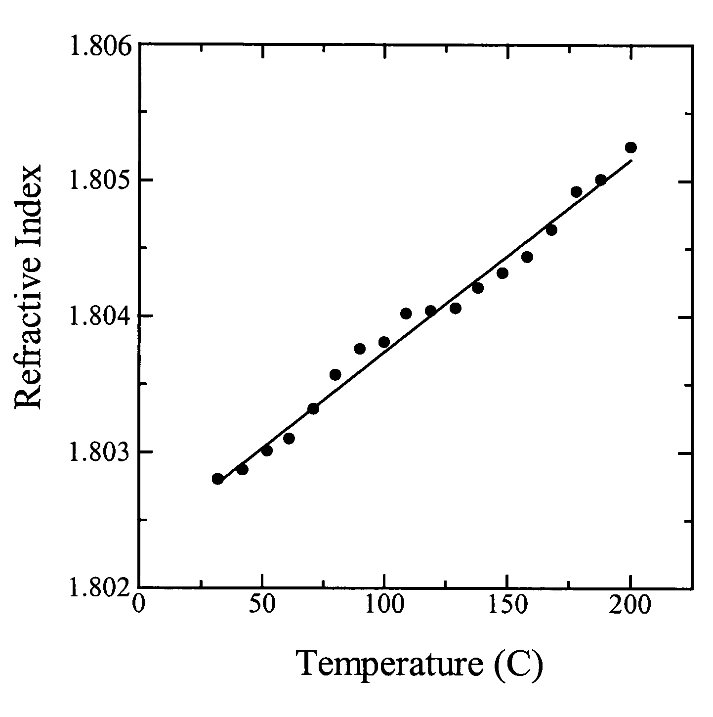
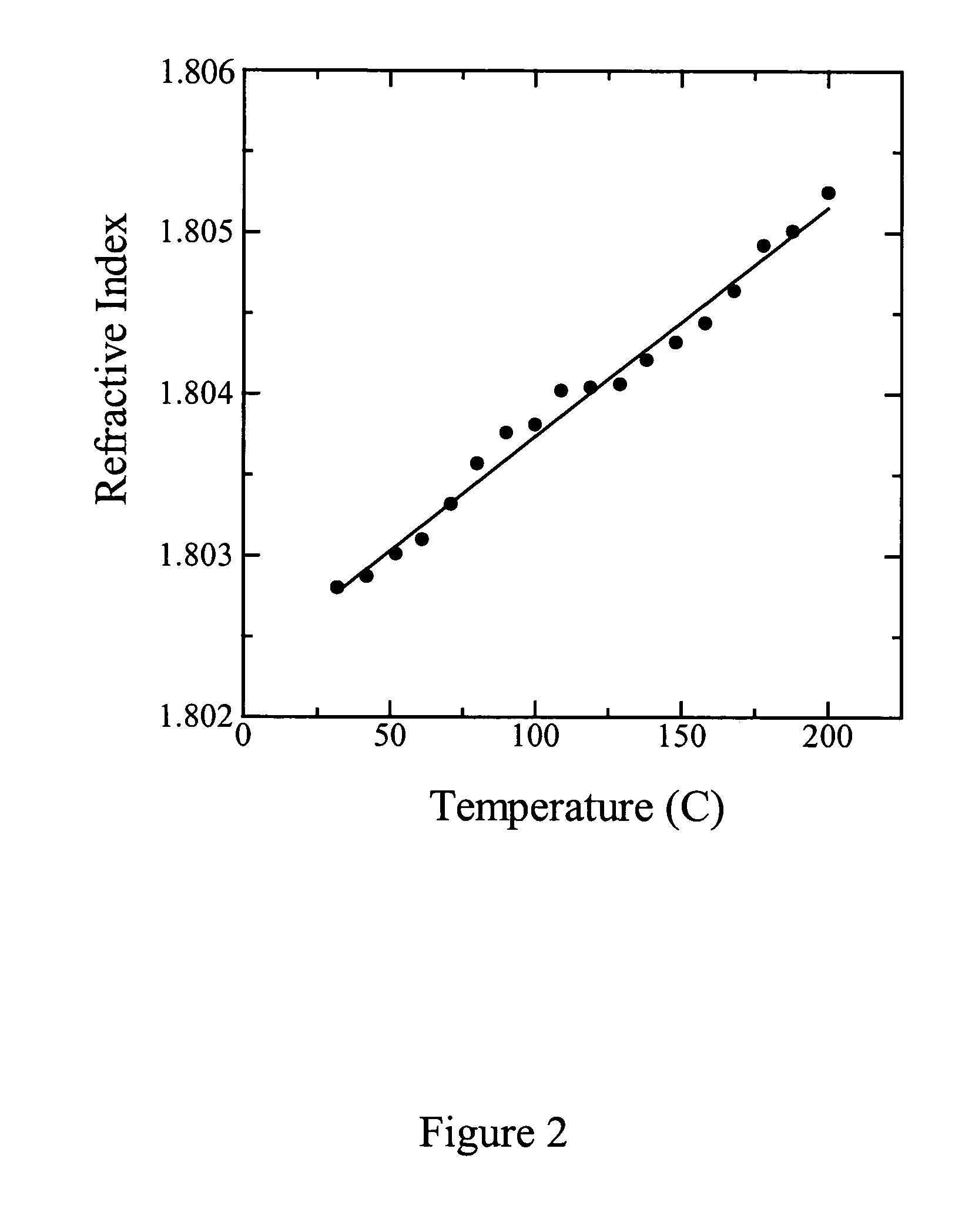
Temperature sensitivity of material properties represents another substantial challenge. Refractive index variations with temperature (dn/dT) cause wavelength shifts and coupling efficiency changes that can disrupt the precise optical interference patterns required for neuromorphic computation. This necessitates either strict thermal management systems or materials with inherently low thermo-optic coefficients.
Fabrication consistency at scale remains problematic, with variations in material deposition, etching, and patterning leading to device-to-device performance differences that undermine the reliability of large-scale neuromorphic systems. Current materials often exhibit property variations that exceed the tight tolerances required for predictable neuromorphic operation.
Finally, long-term material stability presents concerns for deployed systems, with phenomena such as photodarkening, oxidation, and mechanical stress relaxation potentially altering optical properties over time. These aging effects can gradually degrade computational accuracy in neuromorphic circuits, necessitating either more robust materials or compensation mechanisms that add complexity to system design.
Silicon nitride (Si₃N₄) offers lower propagation losses (~0.1 dB/cm) but presents fabrication challenges including film stress management and higher deposition temperatures that complicate integration with electronic components. Meanwhile, silicon-on-insulator (SOI) platforms struggle with polarization-dependent losses and thermal stability issues that affect the consistency of neuromorphic computing operations across varying environmental conditions.
Material interfaces present another significant challenge, as heterogeneous integration of different materials creates junction points where reflection, scattering, and mode mismatch occur. These transition losses can dominate overall system performance, particularly in densely integrated neuromorphic circuits where thousands of components must interact seamlessly.
Nonlinear optical materials essential for mimicking neuronal activation functions face a fundamental trade-off between nonlinearity strength and optical loss. Materials with strong nonlinear responses often exhibit higher absorption, while low-loss materials typically demonstrate weaker nonlinear effects, creating a design constraint that limits computational density and energy efficiency.
Temperature sensitivity of material properties represents another substantial challenge. Refractive index variations with temperature (dn/dT) cause wavelength shifts and coupling efficiency changes that can disrupt the precise optical interference patterns required for neuromorphic computation. This necessitates either strict thermal management systems or materials with inherently low thermo-optic coefficients.
Fabrication consistency at scale remains problematic, with variations in material deposition, etching, and patterning leading to device-to-device performance differences that undermine the reliability of large-scale neuromorphic systems. Current materials often exhibit property variations that exceed the tight tolerances required for predictable neuromorphic operation.
Finally, long-term material stability presents concerns for deployed systems, with phenomena such as photodarkening, oxidation, and mechanical stress relaxation potentially altering optical properties over time. These aging effects can gradually degrade computational accuracy in neuromorphic circuits, necessitating either more robust materials or compensation mechanisms that add complexity to system design.
Current Material Solutions for Low-Loss Waveguides
01 Waveguide design optimization to reduce losses
Various design approaches can be implemented to minimize losses in waveguides. These include optimizing the waveguide geometry, cross-sectional dimensions, and material selection. Specific design features such as tapered structures, curved sections with optimized radii, and specialized junction designs can significantly reduce propagation losses. Advanced modeling techniques help predict and minimize losses before fabrication.- Material selection for reducing waveguide loss: The choice of materials significantly impacts waveguide loss. Low-loss materials such as silicon, silica, and certain polymers can be selected to minimize absorption and scattering losses. Material purity and composition control are essential for reducing imperfections that contribute to propagation losses. Advanced materials with optimized optical properties can be engineered to achieve lower attenuation across specific wavelength ranges.
- Geometric design optimization for waveguides: The geometric design of waveguides plays a crucial role in minimizing losses. Optimizing parameters such as core dimensions, bending radius, and cross-sectional profiles can significantly reduce bending and radiation losses. Tapered structures and adiabatic transitions help minimize mode mismatch losses at junctions and interfaces. Advanced design techniques including mode engineering and topology optimization can be employed to create waveguide structures with inherently lower propagation losses.
- Surface treatment and fabrication techniques: Various surface treatment and fabrication techniques can be employed to reduce waveguide losses. Processes such as chemical mechanical polishing, thermal annealing, and plasma treatment can minimize surface roughness and defects that contribute to scattering losses. Advanced lithography and etching methods enable the creation of smoother sidewalls and more precise structures. Post-fabrication treatments including passivation layers and cladding deposition can further reduce interface scattering and environmental degradation.
- Coupling and interface loss reduction: Coupling losses at interfaces between waveguides and other optical components represent a significant source of overall system loss. Specialized coupling structures such as grating couplers, spot-size converters, and mode adapters can be implemented to improve mode matching and reduce reflection losses. Precision alignment techniques and active alignment systems help minimize misalignment losses. Anti-reflection coatings and index-matching materials can be applied at interfaces to reduce Fresnel reflection losses.
- Novel waveguide structures and technologies: Innovative waveguide structures and emerging technologies offer new approaches to loss reduction. Photonic crystal waveguides utilize periodic structures to control light propagation and reduce certain loss mechanisms. Slot waveguides and subwavelength gratings can enhance light confinement while reducing material absorption losses. Hybrid integration of different material platforms combines the advantages of multiple materials to achieve overall lower loss. Metamaterial-based waveguides with engineered optical properties show promise for ultra-low-loss light transmission in specialized applications.
02 Material selection and processing for low-loss waveguides
The choice of materials and their processing methods significantly impact waveguide losses. High-purity materials with low absorption coefficients are preferred for the core and cladding layers. Advanced deposition techniques, annealing processes, and surface treatments can reduce scattering losses by minimizing defects and roughness at interfaces. Novel composite materials and doping strategies can also be employed to achieve lower propagation losses.Expand Specific Solutions03 Coupling and junction loss reduction techniques
Losses often occur at coupling points and junctions between waveguides or between waveguides and other optical components. Specialized coupling structures, mode matching techniques, and adiabatic transitions can minimize these losses. Precision alignment methods, index matching materials, and specialized coupling geometries help ensure efficient light transfer between components, reducing insertion losses and back-reflections.Expand Specific Solutions04 Planar and integrated waveguide loss reduction
In planar and integrated optical circuits, waveguide losses present unique challenges. Techniques such as sidewall smoothing, specialized etching processes, and protective cladding layers can reduce scattering losses. Integration strategies that minimize the number of interfaces and transitions help maintain signal integrity. Advanced fabrication methods like nanoimprint lithography and precision etching contribute to creating low-loss integrated waveguide structures.Expand Specific Solutions05 Measurement and characterization of waveguide losses
Accurate measurement and characterization of waveguide losses are essential for optimization. Various techniques including cut-back methods, Fabry-Perot resonance analysis, and optical time-domain reflectometry allow precise quantification of propagation, bending, and coupling losses. Advanced imaging and spectroscopic methods help identify loss mechanisms and their spatial distribution. These measurements provide crucial feedback for iterative improvement of waveguide designs and fabrication processes.Expand Specific Solutions
Leading Companies and Research Institutions in Photonic Materials
The neuromorphic chip waveguide materials market is in an early growth phase, characterized by intensive research and development rather than mass commercialization. Current market size remains relatively modest but is projected to expand significantly as neuromorphic computing gains traction in AI applications. From a technical maturity perspective, the field shows varying degrees of advancement among key players. Academic institutions like MIT, Caltech, and Zhejiang University are pioneering fundamental research, while technology companies including Intel, Samsung, and NEC are developing practical implementations. Research organizations such as CNRS and Institut Curie are contributing critical materials science innovations. Companies like Micron and Lumentum are leveraging their expertise in semiconductor and photonics technologies to address the specific challenges of low-loss waveguide materials, focusing on silicon photonics integration and novel material compositions to minimize signal attenuation.
Massachusetts Institute of Technology
Technical Solution: MIT has pioneered silicon photonics integration for neuromorphic computing, developing low-loss waveguides using silicon nitride (Si3N4) with propagation losses as low as 0.1 dB/cm. Their research focuses on CMOS-compatible materials that can be integrated with existing semiconductor fabrication processes. MIT's approach combines thin-film silicon nitride waveguides with phase-change materials to create photonic synapses and neurons. They've demonstrated multi-layer photonic platforms where waveguides are vertically integrated with active neuromorphic components, achieving signal routing with minimal crosstalk. MIT researchers have also explored novel materials like lithium niobate on insulator (LNOI) that offer electro-optic modulation capabilities while maintaining low propagation losses, essential for energy-efficient neuromorphic processing. Their waveguide designs incorporate specialized geometries to minimize bending losses at junctions, critical for dense integration in neuromorphic architectures.
Strengths: Exceptional integration with CMOS fabrication processes, allowing for scalable manufacturing. Advanced multi-layer photonic platforms enable complex 3D neuromorphic architectures. Weaknesses: Some of their advanced material systems require precise deposition techniques that may limit commercial scalability in the near term.
California Institute of Technology
Technical Solution: Caltech has developed proprietary silicon-germanium (SiGe) alloy waveguides for neuromorphic photonic applications, achieving propagation losses below 0.3 dB/cm across the telecommunications C-band. Their research focuses on tailoring material composition to optimize both optical and electronic properties simultaneously. Caltech's approach incorporates gradient-index waveguide structures where the material composition varies spatially to guide light with minimal scattering losses. They've pioneered hybrid integration techniques that combine III-V semiconductor materials with silicon photonics to create efficient light sources directly coupled to low-loss waveguides. Their material platform enables the implementation of wavelength division multiplexing in neuromorphic chips, significantly increasing information processing density. Caltech researchers have also developed specialized cladding materials that not only reduce waveguide losses but also provide thermal stability, addressing one of the key challenges in photonic neuromorphic computing where temperature fluctuations can affect performance.
Strengths: Advanced material engineering capabilities allowing precise control of optical properties. Hybrid integration techniques enable complete photonic neuromorphic systems on a single chip. Weaknesses: Some of their more exotic material combinations may face challenges in scaling to high-volume manufacturing environments.
Key Innovations in Waveguide Material Engineering
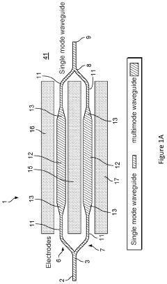
Low-loss waveguiding structures, in particular modulators
PatentPendingUS20240004226A1
Innovation
- A hybrid optical modulator design that incorporates both single mode and multimode waveguide sections, where the multimode sections are adjacent to electrodes, reducing optical loss through the use of tapered transitions to excite only the fundamental mode, thereby minimizing scattering and absorption losses.
Silicon-oxycarbide high index contrast, low-loss optical waveguides and integrated thermo-optic devices
PatentInactiveUS7043133B2
Innovation
- The use of silicon-oxycarbide (SiOC) optical waveguides with refractive indices between 1.5 and 2.5 and a temperature-dependent refractive index change (dn/dT) of 1×10⁻⁵/°C to 3×10⁻⁵/°C, achieved through chemical vapor deposition with tunable film stress and optimized precursor gases, allows for higher refractive index contrasts and reduced power consumption.

Fabrication Techniques for Advanced Waveguide Materials
The fabrication of advanced waveguide materials for neuromorphic chips requires sophisticated techniques that balance precision, scalability, and compatibility with existing semiconductor manufacturing processes. Chemical Vapor Deposition (CVD) remains a cornerstone technique, offering exceptional control over material composition and thickness. For silicon nitride waveguides, Low-Pressure CVD (LPCVD) has demonstrated superior film quality with reduced hydrogen content, resulting in waveguides with propagation losses as low as 0.1 dB/cm at telecom wavelengths.
Atomic Layer Deposition (ALD) has emerged as a critical technique for creating ultra-thin, conformal films with atomic-level precision. This approach enables the deposition of high-quality aluminum oxide and titanium dioxide layers that serve as excellent cladding materials, reducing scattering losses at waveguide interfaces. The self-limiting nature of ALD reactions ensures exceptional uniformity across large wafer surfaces, which is essential for maintaining consistent optical properties throughout neuromorphic circuits.
Physical Vapor Deposition (PVD) techniques, particularly sputtering and electron-beam evaporation, offer versatility in depositing metals and dielectrics for waveguide structures. Magnetron sputtering has proven effective for depositing low-loss silicon nitride and silicon oxynitride films with precisely controlled refractive indices. These techniques allow for rapid material deposition but require careful optimization to minimize surface roughness that could contribute to scattering losses.
Lithographic patterning represents another critical fabrication step, with electron-beam lithography providing the highest resolution for defining nanoscale waveguide structures. For larger-scale production, deep-UV lithography offers a balance between resolution and throughput. The sidewall roughness resulting from etching processes significantly impacts waveguide performance, necessitating advanced etching techniques such as Inductively Coupled Plasma Reactive Ion Etching (ICP-RIE) with optimized chemistry to achieve smooth vertical profiles.
Post-deposition annealing has proven essential for reducing material defects and absorption centers in waveguide materials. High-temperature annealing (800-1100°C) of silicon nitride films can significantly reduce N-H bonds, which are major sources of absorption at telecom wavelengths. Similarly, thermal oxidation processes can be employed to create ultra-smooth interfaces between core and cladding materials, minimizing scattering losses.
Chemical-mechanical polishing (CMP) techniques have become increasingly important for planarizing multilayer waveguide structures in complex neuromorphic architectures. This process enables the creation of vertically integrated photonic layers with minimal topographical variations, facilitating the integration of optical and electronic components on the same chip while maintaining optical performance.
Integration Challenges with Electronic Neuromorphic Components
The integration of photonic waveguides with electronic neuromorphic components presents significant challenges that must be addressed to realize fully functional neuromorphic chips. The fundamental issue stems from the inherent differences between photonic and electronic technologies, each operating on distinct physical principles and manufacturing processes.
Material compatibility represents a primary concern when integrating low-loss waveguide materials with conventional CMOS electronics. Silicon nitride and silicon dioxide waveguides may require deposition temperatures exceeding 300°C, potentially compromising the integrity of underlying electronic components. Conversely, polymer-based waveguides offer lower processing temperatures but may suffer from stability issues when subjected to standard electronic packaging procedures.
Thermal management emerges as another critical challenge. Electronic components generate substantial heat during operation, which can alter the refractive indices of waveguide materials and consequently affect optical signal propagation. This thermal crosstalk necessitates sophisticated thermal isolation strategies or active cooling mechanisms, adding complexity to the overall chip design.
Signal conversion between photonic and electronic domains introduces additional inefficiencies. The electro-optic modulators required for converting electronic signals to optical ones often demand high driving voltages incompatible with low-power neuromorphic computing paradigms. Similarly, photodetectors for the reverse conversion process may introduce latency and energy overhead that diminishes the speed advantages offered by photonic interconnects.
Manufacturing alignment precision presents perhaps the most formidable challenge. Photonic waveguides require sub-micron alignment precision to minimize coupling losses, whereas electronic components typically operate with more relaxed tolerances. This disparity necessitates advanced fabrication techniques such as wafer-scale bonding or monolithic integration approaches that can maintain precise alignment between both domains.
Packaging considerations further complicate integration efforts. Photonic components often require optical access points for external light sources or detectors, creating potential vulnerabilities in hermetic sealing. Additionally, the coefficient of thermal expansion mismatch between various materials can induce mechanical stress during temperature fluctuations, potentially causing waveguide misalignment or even structural failure.
Addressing these integration challenges requires interdisciplinary approaches combining expertise from photonics, electronics, materials science, and thermal engineering. Recent advances in heterogeneous integration techniques and novel materials with dual electronic-photonic functionality show promise for overcoming these obstacles, potentially enabling the next generation of high-performance neuromorphic computing platforms.
Unlock deeper insights with Patsnap Eureka Quick Research — get a full tech report to explore trends and direct your research. Try now!
Generate Your Research Report Instantly with AI Agent
Supercharge your innovation with Patsnap Eureka AI Agent Platform!