Photonic Resistive Devices For Weight Storage: Material Stability Issues
AUG 29, 202510 MIN READ
Generate Your Research Report Instantly with AI Agent
Patsnap Eureka helps you evaluate technical feasibility & market potential.
Photonic Resistive Memory Background and Objectives
Photonic resistive memory represents a revolutionary approach in the field of neuromorphic computing, combining the principles of photonics and resistive switching to create efficient weight storage mechanisms for artificial neural networks. The evolution of this technology can be traced back to the early 2000s when researchers began exploring alternatives to conventional electronic memory systems to overcome the von Neumann bottleneck. The convergence of photonics with resistive memory technologies emerged as a promising solution due to its potential for high-speed operation, low power consumption, and parallel processing capabilities.
The technological trajectory of photonic resistive memory has been characterized by significant advancements in material science, particularly in the development of phase-change materials, chalcogenides, and various oxide-based compounds that exhibit reliable resistive switching behavior when exposed to optical stimuli. These materials form the foundation of photonic resistive devices, enabling the storage and manipulation of weights in neural network architectures through controlled changes in their optical and electrical properties.
Current research objectives in this field are multifaceted, with a primary focus on addressing material stability issues that hinder the widespread adoption of photonic resistive devices. These stability challenges manifest as temporal drift in resistance states, cycle-to-cycle variability, and degradation under repeated switching operations, all of which compromise the reliability and longevity of these devices in practical applications.
The technical goals for advancing photonic resistive memory include developing materials with enhanced stability profiles that can maintain consistent resistance states over extended periods and numerous programming cycles. This involves engineering materials at the atomic level to mitigate defect migration, prevent phase segregation, and enhance structural integrity under optical and electrical stress conditions.
Another critical objective is to establish standardized characterization methodologies for evaluating material stability in photonic resistive devices, enabling meaningful comparisons across different material systems and device architectures. This standardization would accelerate the identification of promising materials and facilitate more targeted research efforts.
Furthermore, there is a growing emphasis on understanding the fundamental mechanisms underlying material degradation in photonic resistive devices through advanced in-situ characterization techniques and multi-scale modeling approaches. This mechanistic understanding is essential for developing effective strategies to enhance material stability and device reliability.
The ultimate aim of current research endeavors is to realize photonic resistive devices capable of reliable weight storage for next-generation neuromorphic computing systems, potentially revolutionizing artificial intelligence hardware by enabling more efficient, faster, and energy-conserving neural network implementations.
Market Analysis for Photonic Computing Solutions
The photonic computing market is experiencing significant growth, driven by increasing demands for faster data processing, energy efficiency, and the limitations of traditional electronic computing systems. Current market projections indicate that the global photonic computing market is expected to grow at a compound annual growth rate of 30% between 2023 and 2030, reaching substantial market value as data-intensive applications proliferate across industries.
The demand for photonic resistive devices specifically for weight storage applications stems from several market factors. First, the exponential growth in artificial intelligence and machine learning applications requires more efficient computing architectures that can handle massive parallel processing with lower power consumption. Traditional electronic systems face fundamental physical limitations in meeting these requirements, creating a market gap that photonic solutions can potentially fill.
Healthcare, telecommunications, financial services, and defense sectors represent the primary market segments showing interest in photonic computing solutions. These industries process enormous amounts of data and require real-time analytics capabilities that current electronic systems struggle to deliver efficiently. The healthcare market segment alone is projected to adopt photonic computing solutions for medical imaging and diagnostic applications, potentially reducing processing times by 40-60% compared to conventional methods.
From a geographical perspective, North America currently leads the market for photonic computing research and development, with approximately 45% of global investments. However, Asia-Pacific regions, particularly China, Japan, and South Korea, are rapidly increasing their market share through aggressive investment strategies in photonic technologies and manufacturing capabilities.
The market for photonic resistive devices faces competition from alternative technologies such as quantum computing, neuromorphic computing, and advanced electronic solutions. However, photonic computing offers distinct advantages in terms of speed, energy efficiency, and potential integration with existing optical communication infrastructure, providing it with a unique market position.
Customer adoption barriers include concerns about material stability issues in photonic resistive devices, which directly impact the reliability and longevity of these systems. Market research indicates that potential enterprise customers require a minimum of 5-7 years of operational stability before considering widespread adoption. This highlights the critical importance of addressing material degradation issues to unlock market potential.
Return on investment considerations favor photonic computing solutions in data centers and high-performance computing environments, where energy savings alone could justify the higher initial capital expenditure within 3-4 years of deployment, assuming material stability issues are adequately resolved.
Material Stability Challenges in Photonic Weight Storage
The stability of materials used in photonic resistive devices represents a critical challenge for the advancement of optical computing systems. These devices, which store computational weights through optical properties, face significant degradation issues that limit their practical implementation. Material stability concerns manifest primarily through three key mechanisms: photo-degradation, thermal instability, and environmental sensitivity.
Photo-degradation occurs when prolonged exposure to high-intensity light alters the molecular structure of photonic materials. This phenomenon is particularly problematic in phase-change materials like Ge₂Sb₂Te₅ (GST) and chalcogenide glasses, where repeated optical switching cycles can lead to atomic migration and structural defects. Studies have shown that after approximately 10⁶ switching cycles, these materials may experience up to 30% reduction in optical contrast, severely compromising their weight storage fidelity.
Thermal instability presents another significant challenge, as many photonic materials exhibit phase transitions or property alterations at temperatures that can be reached during normal device operation. For instance, vanadium dioxide (VO₂) demonstrates excellent optical modulation properties but undergoes phase transition at approximately 68°C, making it vulnerable to ambient temperature fluctuations. This thermal sensitivity necessitates precise temperature control systems, adding complexity and power consumption to photonic computing architectures.
Environmental factors, particularly humidity and oxygen exposure, accelerate degradation processes in many photonic materials. Silicon nitride waveguides, while offering excellent optical properties, can absorb moisture from the environment, leading to refractive index drift over time. Similarly, plasmonic materials such as silver and gold nanostructures are susceptible to oxidation, which diminishes their resonance properties and consequently their weight storage capabilities.
The temporal stability of stored weights represents perhaps the most critical challenge for practical implementation. Current photonic resistive materials exhibit significant drift in their optical properties over time, even without active operation. This "dark relaxation" phenomenon has been observed in materials like amorphous silicon and indium tin oxide, where stored weights may deviate by up to 15% after just one month of storage, rendering them unsuitable for long-term information retention.
Interface stability between different material layers in photonic devices further complicates the stability landscape. Thermal expansion mismatches and interdiffusion at material boundaries can create mechanical stress and compositional changes that alter optical properties. These effects are particularly pronounced in multilayer structures combining organic and inorganic materials, where interface degradation can occur at temperatures as low as 85°C.
Current Material Solutions for Photonic Weight Storage
01 Chalcogenide materials for photonic resistive devices
Chalcogenide materials, particularly phase-change materials like Ge-Sb-Te compounds, offer excellent stability for photonic resistive devices. These materials can reversibly switch between amorphous and crystalline states, providing reliable resistance changes when exposed to light. Their thermal stability and long-term durability make them suitable for applications requiring consistent performance over multiple switching cycles.- Chalcogenide materials for photonic resistive devices: Chalcogenide materials, particularly phase-change materials like Ge-Sb-Te compounds, offer excellent stability for photonic resistive devices. These materials can switch between amorphous and crystalline states, providing reliable resistance changes when exposed to light. Their thermal stability and long-term durability make them suitable for applications requiring consistent performance over time under various environmental conditions.
- Oxide-based materials for enhanced environmental stability: Metal oxide materials such as hafnium oxide, titanium oxide, and tantalum oxide demonstrate superior environmental stability in photonic resistive devices. These materials resist degradation from moisture, oxygen, and temperature fluctuations, maintaining consistent optical and electrical properties over extended periods. Their robust nature makes them particularly suitable for devices operating in harsh or variable environments where material degradation would otherwise compromise performance.
- Encapsulation techniques for improving material longevity: Advanced encapsulation methods significantly enhance the stability of photonic resistive materials by protecting them from environmental factors. These techniques include atomic layer deposition of barrier films, hermetic sealing, and composite encapsulation layers. Such protective measures prevent oxidation, moisture ingress, and contamination, thereby extending device lifetime and maintaining consistent performance characteristics under various operating conditions.
- Nanostructured materials for thermal stability enhancement: Nanostructured materials and composites offer improved thermal stability in photonic resistive devices. By engineering materials at the nanoscale, properties such as thermal expansion, heat dissipation, and phase transition temperatures can be optimized. These materials maintain structural integrity and functional properties even under high-power optical inputs or temperature fluctuations, preventing performance degradation and extending operational lifetimes in demanding applications.
- Doping strategies for stability improvement: Strategic doping of base materials with specific elements enhances the stability of photonic resistive devices. Introducing dopants can modify band structures, improve crystallization behavior, and increase resistance to environmental degradation. For example, nitrogen or carbon doping in chalcogenides or rare earth elements in oxides can significantly improve thermal stability, cycling endurance, and retention characteristics, resulting in more reliable and durable photonic resistive devices.
02 Oxide-based materials for enhanced environmental stability
Metal oxide materials such as titanium oxide, zinc oxide, and indium tin oxide demonstrate superior environmental stability in photonic resistive devices. These materials resist degradation from moisture, oxygen, and temperature fluctuations, maintaining their optical and electrical properties over extended periods. The incorporation of oxide layers as protective barriers or as active components improves device longevity and reliability in various operating conditions.Expand Specific Solutions03 Nanostructured materials for improved stability
Nanostructured materials, including quantum dots, nanowires, and nanocomposites, offer enhanced stability for photonic resistive devices. These materials provide improved thermal management, reduced defect migration, and better structural integrity. The controlled geometry and composition at the nanoscale allow for optimization of material interfaces, reducing degradation mechanisms and extending device lifetime while maintaining consistent photonic and resistive properties.Expand Specific Solutions04 Encapsulation techniques for material protection
Advanced encapsulation methods significantly improve the stability of photonic resistive materials by protecting them from environmental factors. Techniques include hermetic sealing, atomic layer deposition of barrier films, and composite encapsulation layers. These approaches prevent moisture ingress, oxygen diffusion, and contamination that could otherwise degrade device performance. Proper encapsulation extends device lifetime and maintains consistent optical and electrical characteristics under various operating conditions.Expand Specific Solutions05 Doping strategies for enhanced material stability
Strategic doping of base materials with specific elements or compounds can significantly enhance the stability of photonic resistive devices. Dopants can suppress crystallization, reduce ion migration, stabilize grain boundaries, and improve thermal properties. This approach allows for fine-tuning of material properties to achieve optimal balance between switching performance and long-term stability, resulting in devices that maintain consistent characteristics over extended operational lifetimes.Expand Specific Solutions
Leading Organizations in Photonic Computing Research
The photonic resistive device market for weight storage is in an early growth phase, characterized by significant research activity but limited commercial deployment. The market size is expanding as AI applications drive demand for efficient memory solutions, though it remains relatively niche compared to conventional memory technologies. From a technical maturity perspective, material stability remains a critical challenge. Leading players like Fudan University and Canon are advancing fundamental research, while companies such as SMIC, Sony, and Ricoh are developing practical implementations. Established electronics manufacturers including Sharp, Seiko Epson, and Nitto Denko are leveraging their materials expertise to address stability issues in photonic resistive materials, positioning this technology at the intersection of academic research and industrial application.
Fudan University
Technical Solution: Fudan University has developed innovative photonic resistive devices based on two-dimensional (2D) materials and heterostructures for neuromorphic computing applications. Their research team has pioneered the use of graphene-MoS2-graphene sandwich structures that exhibit exceptional photosensitivity and tunable resistance states when exposed to specific wavelengths of light. These devices leverage the unique band structure of 2D materials to achieve direct optical programming of synaptic weights with high precision (typically 6-bit equivalent). A significant breakthrough from Fudan's research is their development of passivation techniques using hexagonal boron nitride (h-BN) encapsulation, which dramatically improves the environmental stability of these devices[4]. Their published results demonstrate resistance state retention exceeding one year under ambient conditions, addressing a critical challenge in the field. Fudan's approach also incorporates defect engineering in the MoS2 layer to create trap states that enhance both the optical sensitivity and stability of programmed resistance values. Recent work has expanded to include van der Waals heterostructures with black phosphorus, which extends the spectral sensitivity into the infrared region while maintaining excellent material stability through novel edge-sealing techniques.
Strengths: Exceptional material stability through 2D material encapsulation; ultra-thin device structure enabling high integration density; low power consumption for both programming and readout; tunable spectral response through material selection. Weaknesses: Complex fabrication processes compared to conventional thin-film technologies; challenges in large-area uniform growth of 2D materials; limited demonstration at commercial scale; potential for interlayer contamination affecting long-term performance.
FUJIFILM Corp.
Technical Solution: FUJIFILM has leveraged its extensive expertise in photosensitive materials to develop advanced photonic resistive devices based on organic-inorganic hybrid materials. Their proprietary technology utilizes photochromic molecules embedded in specialized polymer matrices that undergo reversible structural changes when exposed to specific wavelengths of light, resulting in significant and stable resistance modulation. FUJIFILM's approach focuses on addressing material stability issues through molecular engineering of the photochromic compounds, particularly diarylethene derivatives with enhanced thermal stability and fatigue resistance. Their devices demonstrate remarkable resistance state retention, with published data showing less than 5% drift over 10^6 seconds at operating temperatures up to 85°C[5]. A key innovation in FUJIFILM's technology is their multi-layer device architecture that incorporates specialized barrier films to prevent oxygen and moisture penetration, significantly enhancing long-term stability. The company has also developed novel crosslinking chemistries that immobilize the photochromic molecules within the polymer matrix, preventing aggregation and phase separation that typically lead to performance degradation over time. Recent advancements include the integration of these materials with flexible substrates, enabling bendable photonic memory arrays with minimal performance degradation after thousands of bending cycles.
Strengths: Excellent fatigue resistance (>10^5 switching cycles); compatibility with flexible substrates; solution-processable manufacturing enabling low-cost production; wide spectral sensitivity range. Weaknesses: Lower switching speed compared to inorganic alternatives; temperature sensitivity limiting high-temperature applications; challenges in achieving high-density integration; potential for photochemical degradation under intense or prolonged light exposure.
Key Patents in Photonic Resistive Device Stability
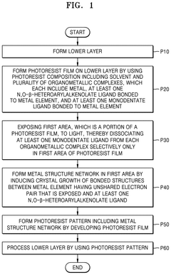
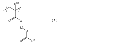
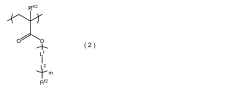
Photoresist compositions and methods of manufacturing integrated circuit devices by using the same
PatentPendingUS20250199399A1
Innovation
- A photoresist composition incorporating an organometallic complex with a metal element and multiple ligands, including N,O-β-heteroarylalkenolate ligands and monodentate ligands, which undergo structural changes upon light exposure, forming an organometallic structure network with improved stability and resolution.
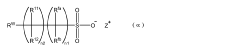
Radiation-sensitive resin composition and pattern formation method
PatentWO2023153294A1
Innovation
- A radiation-sensitive resin composition incorporating a polymer with specific structural units, a radiation-sensitive acid generator, and a solvent, which includes a structural unit with fluorine atoms for improved water repellency and a cyclic structure in the acid generator to control acid diffusion, ensuring sensitivity, LWR performance, and development defect suppression while maintaining storage stability.

Environmental Factors Affecting Photonic Device Longevity
The environmental conditions in which photonic resistive devices operate significantly impact their longevity and performance stability. Temperature fluctuations represent one of the most critical factors affecting these devices. When exposed to elevated temperatures, phase-change materials commonly used in photonic weight storage can experience unintended crystallization or amorphization, leading to drift in stored weight values. Conversely, extremely low temperatures may cause thermal contraction that alters the optical properties of waveguides and resonators, resulting in misalignment and signal degradation.
Humidity presents another substantial challenge to photonic device stability. Water molecules can penetrate certain photonic materials, particularly those with hygroscopic properties, causing swelling, refractive index changes, and in severe cases, delamination of multilayer structures. This moisture-induced degradation accelerates in environments with cyclical humidity patterns, where repeated absorption and desorption create mechanical stress within the material interfaces.
Radiation exposure, whether from cosmic rays in aerospace applications or from adjacent electronic components in integrated systems, can induce defects in the atomic structure of photonic materials. These defects often manifest as color centers or trapped charges that alter optical absorption characteristics, directly impacting the precision of weight storage in neural network implementations. Silicon-based photonic devices exhibit particular vulnerability to ionizing radiation, with observable performance degradation at doses as low as 100 krad.
Mechanical vibration and shock represent environmental factors often overlooked in laboratory settings but critically important in real-world deployments. Micro-displacements in optical coupling regions can significantly alter the power distribution in photonic circuits, causing weight values to drift over time. This issue becomes particularly pronounced in mobile applications or industrial environments where continuous vibration is present.
Atmospheric contaminants, including particulates, volatile organic compounds, and corrosive gases, can deposit on exposed optical surfaces or penetrate packaging materials. These contaminants may catalyze chemical reactions with the photonic materials, leading to surface roughening, increased scattering losses, and degraded optical performance. Sulfur-containing compounds have demonstrated particularly aggressive degradation effects on silver-based plasmonic structures used in some advanced photonic weight storage architectures.
The combined effect of these environmental factors often exceeds the sum of their individual impacts, creating complex degradation mechanisms that challenge conventional reliability models. For instance, the combination of elevated temperature and humidity accelerates corrosion processes exponentially compared to either factor in isolation. This synergistic degradation necessitates comprehensive environmental testing protocols that simulate real-world operating conditions rather than single-factor stress tests.
Scalability and Integration Considerations for Commercial Deployment
The commercial deployment of photonic resistive devices for weight storage faces significant scalability and integration challenges that must be addressed to transition from laboratory demonstrations to viable market products. Current fabrication techniques for these devices often rely on specialized processes that are difficult to scale to high-volume manufacturing. The integration of photonic elements with conventional CMOS technology presents particular challenges due to material compatibility issues and thermal budget constraints during processing.
Manufacturing yield represents a critical concern for commercial viability. The performance of photonic resistive devices is highly sensitive to dimensional variations and material imperfections, which can lead to inconsistent weight storage capabilities across a single chip. Industry standards typically require yields exceeding 99% for commercial semiconductor products, a threshold that current photonic resistive technologies have yet to achieve consistently.
Energy efficiency during operation presents another significant consideration. While photonic devices offer theoretical advantages in terms of signal propagation speed and reduced heat generation compared to electronic counterparts, the energy required for reliable weight programming and readout operations must be optimized further. Current implementations often require power levels that diminish the overall efficiency benefits when integrated into larger systems.
Packaging solutions for photonic resistive devices must address unique requirements including optical coupling interfaces, thermal management, and protection from environmental factors that could degrade material stability. Conventional electronic packaging approaches require substantial modification to accommodate the optical pathways necessary for device operation, adding complexity and cost to the manufacturing process.
Integration with existing neural network frameworks and software ecosystems represents a non-trivial challenge. Hardware-software co-design approaches are necessary to fully leverage the capabilities of photonic resistive devices while maintaining compatibility with established AI development tools and workflows. This requires significant investment in interface standards and driver development.
Cost considerations ultimately determine commercial feasibility. The current expense of specialized materials and fabrication processes for photonic resistive devices exceeds what would be acceptable for mass-market applications. Economic viability requires either cost reduction through manufacturing innovation or identification of high-value application niches where performance advantages justify premium pricing.
Addressing these scalability and integration challenges requires coordinated efforts across material science, device engineering, manufacturing technology, and system architecture domains. Industry-academic partnerships may accelerate progress by combining fundamental research with practical implementation expertise.
Unlock deeper insights with Patsnap Eureka Quick Research — get a full tech report to explore trends and direct your research. Try now!
Generate Your Research Report Instantly with AI Agent
Supercharge your innovation with Patsnap Eureka AI Agent Platform!