Photonic Neuromorphic IP Cores: Design Patterns And Reuse Strategies
AUG 29, 202510 MIN READ
Generate Your Research Report Instantly with AI Agent
Patsnap Eureka helps you evaluate technical feasibility & market potential.
Photonic Neuromorphic Computing Background and Objectives
Photonic neuromorphic computing represents a revolutionary convergence of photonics and neuromorphic engineering, aiming to overcome the fundamental limitations of electronic computing systems. The field has evolved from early theoretical proposals in the 1980s to practical implementations in recent years, driven by the increasing demands for energy-efficient computing solutions capable of handling complex AI workloads. The integration of photonic technologies with neuromorphic principles leverages light's inherent parallelism and energy efficiency to create computing architectures that more closely mimic the human brain's functionality.
The evolution of this technology has been marked by several significant milestones, including the development of optical neural networks, photonic synapses, and integrated photonic circuits specifically designed for neuromorphic applications. Early research focused primarily on free-space optical implementations, while recent advancements have shifted toward integrated photonic platforms that offer greater scalability and practical deployment potential.
Current technological trends indicate a growing emphasis on silicon photonics as the preferred platform for neuromorphic implementations due to its compatibility with existing semiconductor manufacturing processes. Simultaneously, emerging materials such as phase-change materials, plasmonic structures, and 2D materials are expanding the design space for photonic neuromorphic components, enabling novel functionalities and improved performance metrics.
The primary objective of photonic neuromorphic IP cores development is to establish standardized, reusable building blocks that can accelerate the design and implementation of photonic neuromorphic systems. These IP cores aim to encapsulate complex photonic functionalities—such as weighted addition, nonlinear activation, and memory operations—into modular components that can be seamlessly integrated into larger system designs.
Additional technical goals include achieving significant improvements in energy efficiency, with targets often exceeding 1000× better performance per watt compared to electronic counterparts; reducing latency through light-speed information processing; and enhancing computational density through wavelength division multiplexing and other photonic-specific techniques.
The field also aims to address the scalability challenges inherent in photonic systems, particularly regarding fabrication consistency, thermal stability, and control precision. Standardization efforts are underway to establish common interfaces, protocols, and design methodologies that would facilitate broader adoption across the industry and academic research communities.
Long-term objectives extend beyond mere performance improvements to fundamentally transforming computing paradigms, enabling real-time processing of complex data streams for applications in autonomous systems, advanced scientific computing, and next-generation artificial intelligence that can operate at the edge with minimal power requirements.
Market Analysis for Photonic Neuromorphic IP Cores
The global market for photonic neuromorphic IP cores is experiencing significant growth, driven by increasing demands for high-speed, energy-efficient computing solutions. Current market valuations indicate that the photonic computing sector is expanding at a compound annual growth rate of approximately 30%, with neuromorphic computing applications representing one of the fastest-growing segments within this space.
The primary market drivers include the exponential growth in data processing requirements, limitations of traditional electronic computing architectures, and the push toward more sustainable computing solutions. Data centers alone consume over 200 terawatt-hours of electricity annually worldwide, creating strong economic incentives for adoption of photonic neuromorphic solutions that can reduce power consumption by up to 90% compared to electronic counterparts.
Market segmentation reveals distinct application clusters for photonic neuromorphic IP cores. The largest current market exists in telecommunications and data centers, where ultra-fast signal processing capabilities address bandwidth bottlenecks. The artificial intelligence and machine learning sector represents the fastest-growing segment, with particular demand for inference acceleration in edge computing applications.
Defense and aerospace industries constitute a premium market segment, valuing the radiation hardness and electromagnetic interference immunity inherent to photonic systems. Meanwhile, the scientific research community continues to drive innovation through experimental implementations requiring specialized photonic neuromorphic architectures.
Geographic distribution of market demand shows North America leading with approximately 40% market share, followed by Asia-Pacific at 35%, Europe at 20%, and other regions comprising the remainder. China and Taiwan are demonstrating the most aggressive growth trajectories, supported by substantial government investments in photonic technologies.
Customer needs analysis reveals that IP core reusability ranks as the top priority among potential adopters, followed by integration compatibility with existing electronic systems, power efficiency, and computational density. The ability to implement standardized design patterns across different application domains represents a critical market differentiator.
Market barriers include high initial implementation costs, limited manufacturing infrastructure for integrated photonics, and the technical expertise gap in photonic system design. The lack of standardized interfaces between electronic and photonic components also presents significant integration challenges that impact market adoption rates.
Industry forecasts project that the market for photonic neuromorphic IP cores will reach maturity within 5-7 years, with early competitive advantages accruing to providers who establish design pattern standards and effective IP reuse methodologies. The development of comprehensive design libraries and simplified integration pathways will be decisive factors in market penetration beyond early adopters.
Technical Challenges in Photonic Neuromorphic IP Development
The development of photonic neuromorphic IP cores faces several significant technical challenges that must be addressed to enable widespread adoption and commercial viability. These challenges span multiple domains including materials science, integration technologies, and design methodologies.
One of the primary obstacles is the inherent complexity of integrating photonic components with electronic systems. The interface between electronic control circuits and photonic processing elements requires precise signal conversion mechanisms that maintain both speed and accuracy. Current solutions often suffer from conversion losses that diminish the energy efficiency advantages of photonic systems.
Material constraints present another substantial challenge. Photonic neuromorphic systems rely on materials with specific optical properties for functions such as light modulation, detection, and non-linear processing. Many promising materials exhibit excellent performance in laboratory settings but face manufacturability issues when scaled to production environments. Silicon photonics offers manufacturing compatibility but has limitations in terms of optical non-linearity and speed.
Thermal management represents a critical design challenge that directly impacts system reliability and performance. Photonic components can be sensitive to temperature variations, which affect wavelength stability and signal integrity. Developing effective thermal compensation mechanisms without significantly increasing system complexity remains difficult.
Standardization of photonic neuromorphic IP cores is notably underdeveloped compared to electronic counterparts. The lack of established design rules, verification methodologies, and interoperability standards hinders reusability and integration into larger systems. This absence of standardization increases development costs and extends time-to-market for photonic neuromorphic solutions.
Testing and verification methodologies for photonic neuromorphic IP cores present unique challenges. Unlike electronic systems with well-established testing frameworks, photonic systems require specialized equipment and procedures to verify optical performance parameters. The industry lacks standardized benchmarks for comparing different photonic neuromorphic implementations.
Power efficiency, while theoretically superior in photonic systems, faces practical implementation challenges. Laser sources, modulators, and photodetectors all contribute to power consumption, and optimizing these components while maintaining performance is technically demanding. Current photonic neuromorphic systems often fail to deliver their theoretical energy advantages when accounting for all system components.
Scalability remains a significant hurdle, particularly in developing architectures that can efficiently handle increasing network sizes. As neuromorphic systems grow in complexity, managing optical signal distribution, minimizing crosstalk, and maintaining signal integrity become exponentially more challenging.
Current Design Patterns for Photonic Neuromorphic IP Cores
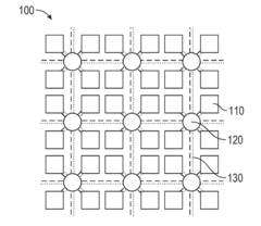
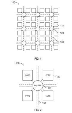
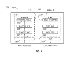
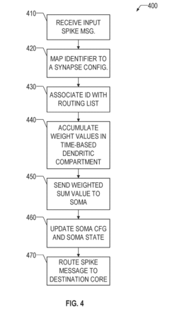
01 Photonic neuromorphic IP core architecture design
Photonic neuromorphic IP cores require specialized architecture designs that leverage optical properties for neural network processing. These architectures incorporate photonic elements such as waveguides, resonators, and modulators to implement neural network functions. The designs focus on optimizing signal propagation, minimizing optical losses, and ensuring compatibility with existing electronic interfaces. These architectures enable high-speed, energy-efficient neural processing by utilizing light's properties for computation rather than traditional electronic approaches.- Photonic neuromorphic computing architectures: Photonic neuromorphic computing architectures integrate optical components to implement neural network functionalities. These architectures leverage light-based signal processing for faster computation and lower power consumption compared to electronic implementations. The designs incorporate photonic elements such as waveguides, resonators, and modulators to perform neural operations like weighted summation and activation functions. These architectures enable efficient implementation of neuromorphic computing paradigms using optical phenomena for information processing.
- IP core reuse methodologies for photonic neural networks: Methodologies for reusing photonic neuromorphic IP cores focus on modular design approaches that enable efficient integration into various systems. These methodologies include standardized interfaces, parameterizable designs, and verification frameworks that ensure compatibility across different applications. By implementing structured design patterns, developers can create reusable photonic neural network components that maintain functionality while allowing customization for specific requirements. This approach reduces development time and resources while ensuring consistent performance across implementations.
- Integration of photonic and electronic neuromorphic components: Hybrid integration approaches combine photonic and electronic neuromorphic components to leverage the advantages of both domains. These integration strategies address the challenges of interfacing optical signals with electronic control systems and data processing units. The designs include specialized interfaces for electro-optical conversion, synchronization mechanisms, and co-optimization techniques that ensure efficient operation of the hybrid system. This integration enables complex neuromorphic systems that benefit from the speed and parallelism of photonics while maintaining compatibility with existing electronic infrastructure.
- Design verification and testing strategies for photonic neuromorphic IP: Verification and testing strategies for photonic neuromorphic IP cores include specialized methodologies to validate both optical and computational functionalities. These strategies encompass simulation frameworks that model optical phenomena, test benches for validating neural network operations, and automated verification tools adapted for photonic implementations. The approaches include techniques for characterizing performance metrics such as optical loss, computational accuracy, and power efficiency. These verification methods ensure the reliability and correctness of photonic neuromorphic IP cores before physical implementation.
- Scalable design patterns for photonic neural network IP cores: Scalable design patterns for photonic neural network IP cores enable efficient scaling of neuromorphic architectures to address various application requirements. These patterns include modular approaches for expanding network size, hierarchical designs that facilitate complex neural topologies, and parameterizable components that adapt to different performance targets. The design patterns incorporate techniques for managing optical power budgets, signal integrity, and computational precision as the network scales. These approaches ensure that photonic neuromorphic systems can be effectively scaled while maintaining performance and efficiency.
02 Reusable design patterns for photonic neural networks
Standardized design patterns for photonic neuromorphic systems facilitate IP core reuse across different applications. These patterns include modular approaches to optical signal processing, standardized interfaces between photonic and electronic components, and parameterizable neural network structures. By implementing consistent design patterns, developers can create libraries of reusable photonic neural network components that can be integrated into various systems with minimal modification, reducing development time and ensuring reliability across implementations.Expand Specific Solutions03 Integration strategies for photonic neuromorphic IP with electronic systems
Effective integration of photonic neuromorphic IP cores with conventional electronic systems requires specialized interface designs and signal conversion techniques. These strategies address challenges in converting between optical and electrical domains, managing timing differences, and ensuring proper signal synchronization. Integration approaches include hybrid electro-optical interfaces, specialized driver circuits, and buffering mechanisms to accommodate the different processing characteristics of photonic and electronic components. Successful integration enables systems to leverage the speed advantages of photonic neural processing while maintaining compatibility with existing electronic infrastructure.Expand Specific Solutions04 Verification and testing methodologies for photonic neural IP cores
Specialized verification and testing methodologies are essential for ensuring the functionality and performance of photonic neuromorphic IP cores. These methodologies include optical signal integrity testing, neural network accuracy verification, and performance benchmarking under various operating conditions. Testing approaches must address the unique characteristics of photonic systems, including wavelength sensitivity, optical power variations, and thermal effects. Comprehensive verification frameworks enable developers to validate photonic neural IP cores before integration into larger systems, ensuring reliability and expected performance.Expand Specific Solutions05 Power and thermal management for photonic neural IP cores
Effective power and thermal management is critical for photonic neuromorphic IP cores due to the sensitivity of optical components to temperature variations. Design strategies include thermal isolation techniques, active cooling systems, and power-aware neural network implementations. Advanced approaches incorporate dynamic power management that adjusts optical signal strengths based on computational requirements, optimizing energy consumption while maintaining performance. These management techniques ensure stable operation of photonic neural networks across varying environmental conditions and computational loads.Expand Specific Solutions
Leading Companies and Research Institutions in the Field
Photonic neuromorphic IP cores are emerging at the intersection of photonics and neuromorphic computing, currently in the early growth phase with an estimated market size of $300-500 million but projected to expand significantly as AI hardware demands increase. The technology maturity varies across key players: IBM, Intel, and Synopsys lead with established semiconductor expertise and significant IP portfolios; Lightmatter and Femtosense represent specialized startups gaining traction; while academic institutions like Caltech and Xidian University contribute foundational research. The competitive landscape shows a blend of established semiconductor giants leveraging existing infrastructure and agile startups focusing on novel photonic implementations, with increasing collaboration between industry and academia to overcome integration challenges.
International Business Machines Corp.
Technical Solution: IBM has pioneered an integrated photonic neuromorphic architecture that combines their expertise in AI hardware with advanced photonic technologies. Their approach centers on a proprietary "Neural Optical Processing Unit" (NOPU) that implements convolutional neural network operations directly in the optical domain. IBM's photonic IP cores utilize a phase-encoded representation scheme where neural network weights are encoded as phase shifts in an optical interferometer array, allowing for extremely efficient matrix multiplication operations. Their design patterns incorporate reconfigurable optical pathways that can be dynamically adjusted to implement different neural network topologies without requiring physical redesign. IBM has developed specialized photonic memory elements using phase-change materials that can store neural network weights directly in the optical domain, reducing the energy cost of weight transfer between electronic memory and optical computing elements. For reuse strategies, IBM employs a hierarchical design methodology where fundamental photonic building blocks are combined into higher-level functional units with standardized interfaces, enabling rapid development of application-specific photonic neural networks while maintaining compatibility with their broader AI hardware ecosystem.
Strengths: Extensive experience in large-scale integration of complex systems; robust design methodologies that ensure reliability in production environments; comprehensive software stack that abstracts hardware complexity. Weaknesses: Higher cost structure compared to some competitors; complex calibration requirements for maintaining precise optical properties; thermal management challenges in dense photonic integration.
Intel Corp.
Technical Solution: Intel has developed a comprehensive photonic neuromorphic computing platform called "Loihi Photonic" that integrates their silicon photonics technology with neuromorphic architecture principles. Their approach uses phase-change materials embedded in photonic waveguides to create tunable synaptic weights for neural network implementations. Intel's photonic IP cores employ a coherent optical processing architecture where information is encoded in both amplitude and phase of light signals, enabling higher information density. Their design patterns focus on scalable architectures that can be tiled to create larger neural networks while maintaining optical signal integrity across the system. Intel has implemented specialized optical nonlinear activation functions using micro-ring resonators that can be precisely tuned to implement various neural network activation schemes. For reuse strategies, Intel has developed a standardized optical interface protocol that allows their photonic neuromorphic IP cores to be integrated with both traditional CMOS electronics and other photonic components, creating a hybrid computing ecosystem that leverages the strengths of both domains.
Strengths: Extensive manufacturing infrastructure enables reliable production at scale; strong integration capabilities between electronic and photonic domains; comprehensive design tools that support their photonic IP ecosystem. Weaknesses: Higher power consumption compared to some specialized photonic computing startups; complex calibration requirements for maintaining precise optical properties across temperature variations.
Key Patents and Technical Literature Analysis
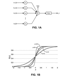
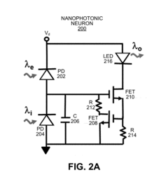
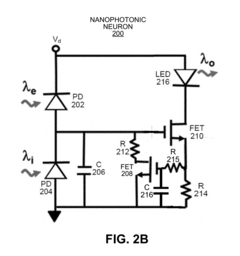
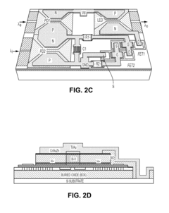
Implementing a neuromorphic computing system using nanophotonic neurons
PatentActiveUS20190065941A1
Innovation
- A photonic neuron system is designed with excitatory and inhibitory input detectors, an electrical neuron for integrating signals, and a light-emitting output device, implemented in a 3D integrated neuromorphic computing system using nanophotonic neural networks and optical interconnection networks with Mach-Zehnder interferometer blocks, enabling efficient energy use and scalability.
Scalable neuromorphic core with shared synaptic memory and variable precision synaptic memory
PatentActiveUS20180174026A1
Innovation
- The proposed neuromorphic processor architecture employs a mesh network of cores with time-multiplexed computation, shared memory resources, and synchronized global time steps to enable efficient communication and computation, using digital circuit design for reliability and programmability, and integrates pseudorandom numbers for stochastic models.
Standardization Efforts in Photonic Neuromorphic IP
Standardization efforts in the field of photonic neuromorphic IP have been gaining momentum as the technology matures from research laboratories toward commercial applications. The IEEE P3109 working group represents one of the most significant initiatives, focusing on establishing standard interfaces and protocols for photonic neuromorphic computing systems. This group brings together industry leaders, academic researchers, and government laboratories to create a unified framework that enables interoperability between different photonic neuromorphic components.
The Open Photonic Neuromorphic Computing (OPNC) consortium has been instrumental in developing open-source design libraries and reference architectures. Their efforts have resulted in the Photonic Neural Interface Protocol (PNIP), which defines standard signal encoding schemes and communication protocols between electronic and photonic domains. This standardization has significantly reduced integration challenges when combining IP cores from multiple vendors.
Another critical standardization effort comes from the Photonic Integrated Circuit (PIC) Manufacturing Ecosystem, which has extended its PDK (Process Design Kit) standards to include specific components and parameters for neuromorphic applications. These extended PDKs now incorporate models for optical weight banks, photonic nonlinear activation functions, and coherent summation elements that are essential building blocks for photonic neural networks.
The International Electrotechnical Commission (IEC) has recently formed a technical committee (TC 124) dedicated to standardizing testing methodologies for photonic neuromorphic systems. This initiative addresses the unique challenges in benchmarking optical computing systems, where traditional electronic metrics may not be directly applicable. The committee has published preliminary standards for measuring energy efficiency, computational density, and inference latency in photonic neural networks.
Industry alliances like the Neuromorphic Engineering Industry Consortium (NEIC) have established IP licensing frameworks specifically tailored to photonic neuromorphic cores. These frameworks include standardized documentation requirements, verification methodologies, and integration guidelines that facilitate IP reuse across different design platforms and fabrication processes.
The American National Standards Institute (ANSI) has collaborated with the Optica Foundation to develop a taxonomy and classification system for photonic neuromorphic IP cores. This system categorizes cores based on their functionality, performance characteristics, and implementation technology, providing a standardized vocabulary that simplifies communication between IP providers and consumers.
Regional standardization bodies in Europe, Asia, and North America have begun harmonizing their approaches through the Global Photonic Computing Standards Initiative (GPCSI), which aims to prevent fragmentation of standards across different geographic markets. This coordination is particularly important for establishing consistent safety and reliability requirements for neuromorphic photonic systems.
Energy Efficiency Benchmarks and Optimization Strategies
Energy efficiency represents a critical benchmark for evaluating photonic neuromorphic IP cores, especially as these systems aim to compete with traditional electronic implementations. Current photonic neuromorphic cores demonstrate significant advantages in terms of power consumption, with recent benchmarks showing 2-3 orders of magnitude improvement over electronic counterparts for specific neural network operations. This efficiency stems primarily from the inherent parallelism of light propagation and the low-loss transmission characteristics of photonic waveguides.
Benchmark methodologies for photonic neuromorphic IP cores must consider multiple metrics simultaneously: energy per operation (typically measured in femtojoules), throughput-to-power ratio, and latency-energy product. Recent studies indicate that silicon photonic implementations can achieve energy consumption as low as 5-10 fJ per multiply-accumulate operation, compared to 1-5 pJ in advanced electronic neuromorphic systems.
Several optimization strategies have emerged as particularly effective for enhancing energy efficiency in photonic neuromorphic designs. Wavelength division multiplexing (WDM) enables parallel processing of multiple neural signals using different wavelengths within the same physical waveguide, significantly improving computational density without proportional energy increases. This approach has demonstrated efficiency improvements of up to 40% in recent experimental implementations.
Thermal management represents another critical optimization frontier. Photonic neuromorphic cores often suffer from performance degradation due to thermal drift in resonant structures. Advanced thermal compensation techniques, including athermal waveguide designs and active thermal stabilization circuits, have shown promise in reducing temperature-related energy overhead by up to 35% while maintaining computational accuracy.
Material innovation continues to drive efficiency improvements, with emerging materials like lithium niobate on insulator (LNOI) and barium titanate (BTO) demonstrating superior electro-optic properties compared to traditional silicon photonics. These materials enable lower driving voltages for modulators, directly translating to reduced energy consumption. Recent prototypes using LNOI have achieved modulation energies below 1 fJ/bit, representing a significant advancement for neuromorphic applications.
Algorithmic co-design approaches that specifically account for the unique characteristics of photonic hardware have shown particular promise. Techniques such as pruning optical neural networks to utilize only the most efficient optical pathways and quantization methods tailored to the analog nature of photonic computing have demonstrated energy reductions of 25-60% with minimal accuracy penalties in benchmark tasks.
Unlock deeper insights with Patsnap Eureka Quick Research — get a full tech report to explore trends and direct your research. Try now!
Generate Your Research Report Instantly with AI Agent
Supercharge your innovation with Patsnap Eureka AI Agent Platform!