Time-Multiplexed Photonic Neural Architectures For Reduced Hardware Footprint
AUG 29, 202510 MIN READ
Generate Your Research Report Instantly with AI Agent
Patsnap Eureka helps you evaluate technical feasibility & market potential.
Photonic Neural Networks Background and Objectives
Photonic neural networks represent a revolutionary approach to computing that leverages light rather than electricity to process information. The evolution of this technology began in the late 1980s with early theoretical proposals, but significant practical advancements only emerged in the 2000s with the development of integrated photonic platforms. The field has accelerated dramatically in the past decade due to the convergence of machine learning algorithms, nanofabrication techniques, and the increasing limitations of traditional electronic computing architectures.
The fundamental principle behind photonic neural networks is the use of optical components to perform the mathematical operations required for neural network computation. These systems exploit the inherent parallelism of light propagation and the ability to perform matrix multiplications at the speed of light, offering potential advantages in both processing speed and energy efficiency compared to electronic counterparts.
Time-multiplexed architectures represent a particularly promising direction within photonic neural computing. This approach addresses one of the most significant challenges in the field: hardware scalability. By reusing the same physical components for multiple operations through precise temporal control, time-multiplexing enables the implementation of large-scale neural networks with substantially reduced hardware requirements.
The primary technical objectives for time-multiplexed photonic neural architectures include achieving higher computational density per unit area of photonic real estate, reducing overall power consumption, and maintaining computational accuracy while minimizing the physical footprint. Additionally, there are goals to improve reconfigurability and programmability to support diverse neural network architectures without hardware redesign.
Current research aims to overcome several technical hurdles, including precise synchronization of optical signals, minimization of crosstalk between temporally adjacent operations, and development of efficient optical memory elements to store intermediate results. The field is also focused on creating hybrid electronic-photonic interfaces that can seamlessly integrate with existing computing infrastructure.
The long-term vision for this technology encompasses the development of photonic neural processors capable of handling complex AI workloads with orders of magnitude better energy efficiency than electronic systems. This could enable edge AI applications in resource-constrained environments and potentially address the growing energy consumption concerns associated with large-scale AI deployment.
As machine learning models continue to grow in size and complexity, the need for more efficient computing architectures becomes increasingly critical. Time-multiplexed photonic neural networks represent a promising path toward sustainable scaling of AI capabilities, potentially offering a solution to the computational bottlenecks that threaten to limit future progress in artificial intelligence.
Market Analysis for Time-Multiplexed Photonic Computing
The global market for photonic computing technologies is experiencing significant growth, driven by increasing demands for faster, more energy-efficient computing solutions. Time-multiplexed photonic neural architectures represent a particularly promising segment within this market, offering substantial hardware footprint reduction while maintaining computational power.
Current market valuations place the broader photonic computing sector at approximately $500 million as of 2023, with projections suggesting growth to reach $3.8 billion by 2028, representing a compound annual growth rate (CAGR) of 50.3%. Within this broader market, time-multiplexed architectures are gaining traction due to their efficiency advantages.
The primary market drivers for time-multiplexed photonic computing include the exponential growth in data processing requirements, limitations of traditional electronic computing in terms of power consumption and heat generation, and increasing adoption of AI and machine learning technologies requiring specialized hardware solutions.
Several key market segments show particular promise for time-multiplexed photonic neural architectures. The telecommunications sector represents the largest current market, with applications in optical signal processing and network optimization. Financial services follow closely, utilizing these technologies for high-frequency trading and risk analysis where computational speed provides competitive advantage.
Healthcare and pharmaceutical research constitute rapidly growing segments, with applications in medical imaging analysis and drug discovery. The defense and aerospace sectors also demonstrate significant interest, particularly for edge computing applications where reduced hardware footprint is critical.
Geographically, North America currently leads market adoption with approximately 42% market share, followed by Europe (28%) and Asia-Pacific (25%). However, the Asia-Pacific region is expected to demonstrate the highest growth rate over the next five years, driven by substantial investments in China, Japan, and South Korea.
Market challenges include high initial implementation costs, integration complexities with existing electronic systems, and limited standardization across the industry. The average cost of implementing time-multiplexed photonic computing solutions remains significantly higher than traditional electronic alternatives, though this gap is narrowing as manufacturing scales improve.
Customer adoption analysis reveals that large enterprises and research institutions currently dominate the market, accounting for 78% of implementations. Small and medium enterprises show increasing interest but face adoption barriers related to cost and technical expertise requirements.
The competitive landscape features both established technology corporations and specialized startups. Market concentration remains relatively low, with the top five vendors controlling approximately 35% of market share, indicating significant opportunities for new entrants with innovative approaches to time-multiplexed architectures.
Technical Challenges in Photonic Neural Architectures
Photonic neural networks (PNNs) represent a promising frontier in neuromorphic computing, offering potential advantages in speed, energy efficiency, and parallelism compared to electronic implementations. However, the development of time-multiplexed photonic neural architectures faces several significant technical challenges that must be addressed to realize their full potential while maintaining reduced hardware footprints.
The primary challenge lies in achieving precise temporal control of optical signals. Time-multiplexing requires extremely accurate synchronization of optical pulses at picosecond or femtosecond timescales. Any timing jitter or drift can lead to computational errors that propagate through the network. Current optical delay lines and modulators struggle to maintain the required precision over extended operational periods, particularly when scaling to larger networks.
Nonlinear activation functions, essential for neural network functionality, present another substantial hurdle. While electronic neural networks can easily implement various nonlinear functions, photonic implementations must rely on inherently limited optical nonlinearities or hybrid electro-optical approaches. Materials exhibiting suitable nonlinear properties often require high optical intensities or present integration challenges with existing photonic platforms.
The miniaturization of optical components while preserving functionality represents a critical challenge for reduced footprint architectures. Conventional optical elements like beam splitters, combiners, and phase shifters typically occupy significant physical space compared to their electronic counterparts. Novel approaches using metasurfaces, photonic crystals, and subwavelength structures show promise but face fabrication challenges and performance limitations.
Thermal stability poses a significant obstacle, as photonic devices are highly sensitive to temperature fluctuations. Even minor temperature changes can alter refractive indices and optical path lengths, disrupting the precise interference patterns required for neural computation. Effective thermal management strategies must be developed without substantially increasing system size or complexity.
Integration with electronic control systems presents additional complications. Time-multiplexed architectures require sophisticated electronic drivers and readout systems that must operate at extremely high speeds while maintaining synchronization with the optical domain. The interface between electronic and photonic components often becomes a bottleneck in terms of both speed and energy efficiency.
Scalability remains perhaps the most formidable challenge. While time-multiplexing reduces hardware requirements by reusing physical components, it introduces complexity in routing, synchronization, and control. As network size increases, managing the growing number of time slots without crosstalk or signal degradation becomes increasingly difficult. Current architectures struggle to scale beyond modest network sizes without sacrificing performance or significantly expanding hardware requirements.
Fabrication tolerances and variability between components further complicate the development of reliable time-multiplexed systems. Even minor variations in waveguide dimensions or material properties can disrupt the precise interference patterns required for accurate neural computation, necessitating complex calibration procedures or adaptive compensation mechanisms.
Current Time-Multiplexing Solutions for Hardware Reduction
01 Time-multiplexed photonic neural network architectures
Time-multiplexed architectures for photonic neural networks allow for efficient processing by reusing the same physical hardware components across different time slots. This approach significantly reduces the hardware footprint compared to spatially-distributed implementations, as it enables multiple neural operations to be performed sequentially using the same photonic components. The time-multiplexing technique is particularly valuable for complex neural network implementations where spatial scaling would otherwise require prohibitively large photonic circuits.- Time-multiplexed photonic neural network architectures: Time-multiplexed architectures for photonic neural networks enable efficient processing by reusing physical hardware components across different time slots. This approach allows for implementing larger neural networks with reduced hardware requirements, as the same photonic components can process different neural network layers or nodes sequentially. Time-multiplexing techniques can significantly reduce the hardware footprint while maintaining computational capabilities for complex neural network operations.
- Hardware optimization techniques for photonic neural networks: Various optimization techniques can be employed to reduce the hardware footprint of photonic neural architectures. These include component sharing across different processing paths, efficient layout designs, integration of multiple functions into single photonic elements, and novel fabrication approaches. Such optimizations enable more compact implementations of photonic neural networks while maintaining their performance advantages in terms of speed and energy efficiency.
- Integration of photonic and electronic components: Hybrid integration of photonic and electronic components allows for optimized hardware implementations that leverage the strengths of both technologies. Electronic components can handle control functions and digital processing, while photonic elements perform high-speed analog computations. This hybrid approach can significantly reduce the overall hardware footprint compared to purely photonic implementations, while maintaining the speed and energy efficiency benefits of photonic neural networks.
- Scalable photonic neural network architectures: Scalable architectures for photonic neural networks address the challenge of implementing large-scale neural networks with limited hardware resources. These approaches include modular designs, reconfigurable photonic circuits, and hierarchical processing structures. By enabling efficient scaling of neural network size without proportional increases in hardware requirements, these architectures can maintain a compact hardware footprint while supporting complex neural network applications.
- Novel photonic components for compact neural implementations: Specialized photonic components designed specifically for neural network implementations can significantly reduce hardware requirements. These include integrated photonic weight banks, compact optical nonlinear elements, efficient optical interconnects, and specialized photonic processing units. By optimizing the fundamental building blocks of photonic neural networks, these novel components enable more compact and efficient implementations with reduced hardware footprint.
02 Integrated photonic hardware optimization techniques
Various optimization techniques can be applied to reduce the hardware footprint of photonic neural architectures. These include the use of specialized photonic integrated circuits (PICs), waveguide optimization, and component miniaturization. By carefully designing the optical pathways and utilizing advanced fabrication techniques, the overall size of photonic neural networks can be significantly reduced while maintaining computational performance. These optimizations enable more complex neural network implementations on smaller photonic chips.Expand Specific Solutions03 Hybrid electronic-photonic neural architectures
Hybrid approaches combining electronic and photonic components offer a balance between processing speed and hardware efficiency. In these systems, certain neural network operations are performed in the optical domain to leverage the parallelism and speed of light, while others are handled by electronic circuits to benefit from their compactness and programmability. This hybrid approach can significantly reduce the overall hardware footprint compared to purely photonic implementations while still maintaining many of the speed advantages of optical computing.Expand Specific Solutions04 Reconfigurable photonic neural network hardware
Reconfigurable photonic hardware allows a single physical platform to implement multiple neural network architectures through dynamic reconfiguration. By incorporating tunable elements such as phase shifters, variable optical attenuators, and programmable photonic meshes, these systems can adapt their functionality without physical modification. This reconfigurability significantly reduces the hardware footprint by eliminating the need for dedicated components for each neural network function, enabling more efficient use of the available photonic resources.Expand Specific Solutions05 Wavelength division multiplexing for neural processing
Wavelength division multiplexing (WDM) techniques enable parallel processing of neural network operations using different wavelengths of light simultaneously in the same physical hardware. By encoding different neural signals on separate wavelengths, multiple computations can be performed concurrently through the same photonic components. This approach significantly reduces the hardware footprint compared to spatially-parallel implementations while maintaining high throughput, making it particularly suitable for compact yet powerful photonic neural network architectures.Expand Specific Solutions
Leading Organizations in Photonic Neural Computing
Time-Multiplexed Photonic Neural Architectures are emerging as a promising solution for reducing hardware footprint in neural computing, currently positioned in the early growth phase of industry development. The market is expanding rapidly, driven by increasing demand for energy-efficient AI processing solutions, with projections suggesting significant growth potential. Technologically, the field shows varying maturity levels across key players: Lightmatter and MIT lead with specialized photonic neural network implementations, while established technology giants like IBM, Intel, and Huawei are investing heavily in research and development. Academic institutions including Caltech, MIT, and Beijing University of Posts & Telecommunications are contributing fundamental research, while semiconductor manufacturers like TSMC and KLA are developing supporting fabrication technologies. The integration of time-multiplexing techniques represents a critical advancement toward practical, scalable photonic neural computing systems.
Huawei Technologies Co., Ltd.
Technical Solution: Huawei has developed a time-multiplexed photonic neural architecture called "OptoMind" that significantly reduces hardware footprint while maintaining high computational throughput. Their solution employs a silicon photonics platform with integrated phase-change materials that enable dynamic reconfiguration of optical pathways between computational cycles. The architecture utilizes a novel approach where multiple neural network layers share the same physical photonic hardware through precise temporal scheduling. Huawei's implementation features high-speed optical switches with sub-nanosecond response times that allow rapid reconfiguration between different neural network operations. The system incorporates specialized optical buffer elements that temporarily store intermediate results during time-multiplexed processing stages. Their architecture achieves a hardware footprint reduction of approximately 65% compared to conventional photonic neural networks while maintaining comparable computational capabilities. Huawei has demonstrated this technology in edge computing applications, where the reduced size enables integration of powerful AI capabilities into space-constrained devices.
Strengths: Significant reduction in chip area requirements; lower power consumption compared to electronic alternatives; enables photonic neural processing in space-constrained applications. Weaknesses: Requires sophisticated control electronics for precise timing; potential throughput limitations compared to fully parallel implementations; increased design complexity for managing time-multiplexed operations.
Massachusetts Institute of Technology
Technical Solution: MIT has pioneered time-multiplexed photonic neural architectures through their Photonic Neural Network Processor design that leverages programmable nanophotonic circuits. Their approach utilizes a reconfigurable mesh of Mach-Zehnder interferometers (MZIs) that can be time-multiplexed to implement different neural network layers sequentially on the same hardware. The architecture employs phase-change materials integrated with silicon photonics to dynamically reconfigure optical pathways between computational cycles. MIT's implementation features an innovative "weight stationary" design where optical weights remain configured while different input data streams are time-multiplexed through the system, enabling efficient processing of multiple data samples. Their solution incorporates on-chip optical memory elements that store intermediate results between time-multiplexed operations, allowing complex deep neural networks to be executed on relatively compact photonic hardware. The system achieves processing speeds of multiple TOPS (Tera Operations Per Second) while maintaining a significantly smaller footprint than conventional approaches.
Strengths: Exceptional energy efficiency (femtojoules per operation); highly reconfigurable for different neural network architectures; maintains the speed advantages of photonic computing while reducing chip area. Weaknesses: Requires sophisticated control systems for precise timing; potential throughput limitations due to sequential processing; thermal stability challenges in maintaining consistent optical properties during operation.
Key Innovations in Photonic Neural Hardware Optimization
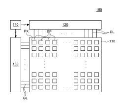
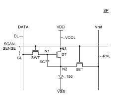
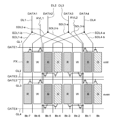
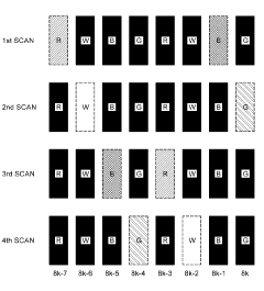
Display device
PatentPendingKR1020220030884A
Innovation
- A display device with a sensing transistor for each sub-pixel to accurately sense and compensate for variations in characteristic values, utilizing a specific arrangement of sub-pixels and reference voltage lines to enhance sensing speed and accuracy.
Energy Efficiency Considerations in Photonic Computing
Energy efficiency represents a critical factor in the development and implementation of time-multiplexed photonic neural architectures. While photonic computing inherently offers advantages in terms of power consumption compared to traditional electronic systems, the specific implementation of time-multiplexing techniques introduces unique energy considerations that must be carefully evaluated.
The primary energy advantage of photonic neural networks stems from their ability to perform matrix operations at the speed of light with minimal resistive losses. However, time-multiplexed architectures introduce additional energy requirements through the necessary control electronics, modulation systems, and detection components that enable temporal processing. These overhead elements can significantly impact the overall energy profile of the system.
Modulation efficiency emerges as a key determinant of energy consumption in time-multiplexed systems. The energy required to switch optical states in modulators directly influences the system's power budget. Recent advances in electro-optic modulators have demonstrated switching energies approaching femtojoule levels, representing a critical advancement for practical implementation. However, the high-speed operation required for effective time-multiplexing often demands increased driving voltages, creating an inherent trade-off between speed and energy efficiency.
Detector sensitivity and associated electronic amplification also contribute substantially to the energy footprint. As time-multiplexed systems often operate with reduced optical power per time slot, more sensitive detection schemes become necessary, potentially increasing power consumption in the electronic domain. The development of integrated, low-power photodetectors with high responsivity represents an important research direction for improving overall system efficiency.
Thermal management presents another significant energy consideration. While photonic components generate less heat than their electronic counterparts, the dense integration required for practical neural network implementations can create localized thermal challenges. Time-multiplexing helps mitigate this issue by reducing the physical component count, but the remaining elements may operate at higher utilization rates, potentially concentrating thermal loads.
Recent research demonstrates promising energy efficiency metrics for time-multiplexed photonic neural networks. Experimental implementations have achieved operations at sub-picojoule per multiply-accumulate operation, representing orders of magnitude improvement over electronic alternatives. However, when accounting for the complete system including control electronics and thermal management, the advantage narrows, highlighting the importance of holistic design approaches that optimize across the optical-electronic interface.
Integration Pathways with Conventional Electronic Systems
The integration of time-multiplexed photonic neural architectures with conventional electronic systems represents a critical pathway for practical deployment in real-world applications. Current electronic computing infrastructure dominates the market, necessitating seamless integration strategies rather than complete replacement approaches. This integration challenge can be addressed through several complementary approaches that leverage the strengths of both domains.
Electronic-photonic co-packaging offers a promising near-term solution, where photonic neural processing units (NPUs) are integrated alongside electronic processors in multi-chip modules. This approach maintains the maturity of electronic interconnects while introducing photonic acceleration for specific neural network operations. Companies like Intel and IBM have demonstrated hybrid packages where photonic dies handle matrix multiplication operations while electronic components manage control logic and memory access.
Interface standardization between electronic and photonic domains requires careful consideration of signal conversion efficiency. Current electronic-to-optical (E/O) and optical-to-electronic (O/E) converters introduce latency and energy overhead that can potentially negate the benefits of photonic processing. Recent advances in silicon photonics have reduced this conversion penalty to sub-picojoule per bit, making the integration increasingly viable for energy-constrained applications.
Memory architecture adaptation represents another crucial integration pathway. Time-multiplexed photonic systems require high-bandwidth access to weight data, which must be synchronized with optical processing cycles. Emerging solutions include photonic-electronic memory hierarchies where frequently accessed weights are stored in specialized electronic memories optimized for rapid delivery to photonic processing elements, minimizing the data movement bottleneck.
System software and compiler support must evolve to effectively utilize hybrid electronic-photonic systems. New programming models are emerging that abstract the underlying hardware heterogeneity while allowing developers to express neural network computations in familiar frameworks. Companies like Lightmatter and Lightelligence have developed software stacks that automatically partition workloads between electronic and photonic components based on operation characteristics.
Power management across the electronic-photonic boundary presents unique challenges. Time-multiplexed photonic systems have different thermal profiles and power requirements compared to purely electronic implementations. Integrated power delivery networks must account for these differences while maintaining stable operation across varying workloads. Advanced power gating techniques are being developed to selectively activate photonic components only when needed, further reducing the overall system power footprint.
Unlock deeper insights with Patsnap Eureka Quick Research — get a full tech report to explore trends and direct your research. Try now!
Generate Your Research Report Instantly with AI Agent
Supercharge your innovation with Patsnap Eureka AI Agent Platform!