Low-Power Photonic Neurons: Materials And Device Architectures
AUG 29, 20259 MIN READ
Generate Your Research Report Instantly with AI Agent
Patsnap Eureka helps you evaluate technical feasibility & market potential.
Photonic Neuron Technology Background and Objectives
Photonic neurons represent a revolutionary approach to neuromorphic computing, emerging from the convergence of photonics and neural network technologies. The concept dates back to the early 2000s when researchers began exploring alternatives to traditional electronic neural networks to overcome the von Neumann bottleneck and energy efficiency limitations. The field has gained significant momentum over the past decade as advances in integrated photonics, nonlinear optical materials, and fabrication techniques have made practical implementations increasingly feasible.
The evolution of photonic neuron technology has been driven by the fundamental advantages of light-based computation: higher bandwidth, reduced latency, and potentially lower energy consumption compared to electronic counterparts. Early photonic neuron designs primarily focused on proof-of-concept demonstrations using discrete optical components. The field has since progressed toward integrated solutions that leverage silicon photonics, III-V semiconductors, phase-change materials, and emerging two-dimensional materials.
Current technological trends point toward the development of ultra-low power photonic neurons that can operate at femtojoule energy levels per operation, representing orders of magnitude improvement over electronic neurons. This trend aligns with the growing demand for energy-efficient computing solutions for artificial intelligence and machine learning applications, where power consumption has become a critical bottleneck.
The primary objective of low-power photonic neuron research is to develop materials and device architectures that can perform neural computations with minimal energy consumption while maintaining high speed and reliability. Specific goals include achieving sub-femtojoule energy consumption per operation, picosecond response times, and high integration density comparable to electronic circuits.
Additional objectives include developing fabrication processes compatible with CMOS technology to enable hybrid electro-photonic systems, enhancing the nonlinear optical properties of materials to improve neuron functionality, and creating scalable architectures for large-scale neuromorphic systems. Researchers also aim to demonstrate practical applications in pattern recognition, signal processing, and high-speed data analysis.
The long-term vision for photonic neuron technology encompasses the creation of fully optical neural networks capable of processing information at the speed of light with minimal energy consumption. This would enable new paradigms in computing, particularly for applications requiring real-time processing of massive data streams, such as autonomous vehicles, advanced robotics, and next-generation telecommunications systems.
Market Analysis for Low-Power Neuromorphic Computing
The neuromorphic computing market is experiencing significant growth, driven by the increasing demand for AI applications and the limitations of traditional computing architectures. Current market valuations place the global neuromorphic computing sector at approximately $3.2 billion in 2023, with projections indicating a compound annual growth rate (CAGR) of 24.7% through 2030. This rapid expansion reflects the urgent need for energy-efficient computing solutions capable of handling complex AI workloads.
Low-power photonic neurons represent a particularly promising segment within this market. The demand for these technologies is primarily fueled by data centers and cloud service providers seeking to reduce their enormous energy consumption. With data centers currently consuming about 1-2% of global electricity and projected to reach 8% by 2030, the market pressure for energy-efficient computing alternatives is substantial.
The industrial sector presents another significant market opportunity, with manufacturing companies increasingly implementing edge AI solutions that require energy-efficient neuromorphic systems. Market research indicates that approximately 67% of manufacturing companies are planning to increase their investments in edge computing technologies over the next three years.
Healthcare applications constitute a rapidly growing market segment for neuromorphic computing, particularly for medical imaging analysis, patient monitoring systems, and drug discovery processes. The healthcare AI market, valued at $11 billion in 2023, is expected to grow at a CAGR of 37% through 2027, creating substantial opportunities for low-power neuromorphic solutions.
Automotive and autonomous systems represent another key market driver, with the need for real-time processing of sensor data while maintaining low power consumption. The automotive AI hardware market is projected to reach $15 billion by 2025, with neuromorphic computing potentially capturing a significant portion of this growth.
Regional market analysis reveals that North America currently holds the largest market share (approximately 42%) in neuromorphic computing, followed by Europe (27%) and Asia-Pacific (23%). However, the Asia-Pacific region is expected to witness the highest growth rate over the next five years due to increasing investments in AI research and semiconductor manufacturing capabilities in countries like China, Japan, and South Korea.
Market barriers include the high initial development costs, technical complexity of implementation, and competition from established computing paradigms. Despite these challenges, the compelling value proposition of dramatically reduced power consumption (potentially 100-1000x improvement over conventional systems) continues to drive market interest and investment in photonic neuromorphic computing technologies.
Current Challenges in Photonic Neural Networks
Despite the significant advancements in photonic neural networks, several critical challenges continue to impede their widespread adoption and practical implementation. The fundamental challenge remains the high power consumption of current photonic neuron architectures. While photonics offers theoretical advantages in energy efficiency compared to electronic systems, practical implementations often suffer from excessive power requirements due to inefficient light-matter interactions and conversion losses at electronic-photonic interfaces.
Material limitations present another significant hurdle. Current photonic neurons rely heavily on materials with suboptimal nonlinear optical properties, requiring high optical intensities to achieve the necessary nonlinear responses. This contradicts the goal of developing low-power systems. Additionally, many promising materials exhibit desirable properties only under specific conditions, such as cryogenic temperatures, making practical deployment challenging.
Integration density remains substantially behind electronic counterparts. The diffraction limit fundamentally constrains the miniaturization of photonic components, resulting in photonic neurons that occupy significantly larger footprints than their electronic equivalents. This limitation severely impacts scalability for complex neural network architectures requiring millions of neurons.
The fabrication complexity of photonic neural networks presents another substantial barrier. Current manufacturing processes for integrated photonics lack the maturity and standardization of electronic semiconductor fabrication. Variations in manufacturing processes lead to device inconsistencies, affecting the reliability and reproducibility of photonic neural networks.
Thermal management issues further complicate photonic neuron design. Many photonic materials and devices are highly temperature-sensitive, with performance characteristics changing significantly with temperature fluctuations. This necessitates sophisticated thermal control systems, adding complexity and power overhead.
The lack of standardized design methodologies and tools specifically tailored for photonic neural networks hinders rapid development and optimization. While electronic neural networks benefit from decades of established design frameworks, photonic counterparts lack equivalent support infrastructure.
Finally, the challenge of interfacing photonic neural networks with existing electronic systems creates significant overhead. The energy and latency costs associated with optical-electrical-optical conversions can negate the inherent advantages of photonic processing, particularly for applications requiring frequent data exchange with conventional electronic systems.
Addressing these challenges requires interdisciplinary approaches spanning materials science, device physics, integrated photonics, and neural network architecture design to realize the full potential of low-power photonic neurons.
State-of-the-Art Low-Power Photonic Neuron Implementations
01 Energy-efficient photonic neural networks
Photonic neurons offer significant power consumption advantages over traditional electronic neural networks. By using light for computation instead of electricity, these systems can process information with minimal energy loss. The architecture typically includes optical waveguides, modulators, and photodetectors that work together to perform neural network operations while consuming orders of magnitude less power than conventional electronic implementations.- Low power consumption in photonic neural networks: Photonic neurons offer significant advantages in power efficiency compared to traditional electronic neural networks. By utilizing light for computation and signal transmission, these systems can achieve ultra-low power consumption while maintaining high processing speeds. The optical processing eliminates resistive heating issues common in electronic systems, allowing for more energy-efficient neural network implementations that are particularly valuable for edge computing and mobile applications.
- Power management techniques for optical neural systems: Various power management techniques have been developed specifically for photonic neural networks to optimize their energy efficiency. These include selective activation of optical components, dynamic power scaling based on computational load, and sleep/wake protocols for optical elements. Advanced power control circuits monitor and adjust the energy consumption of photonic neurons in real-time, ensuring minimal power usage while maintaining computational performance.
- Integration of photonic neurons with conventional electronics: Hybrid systems that combine photonic neurons with conventional electronic components offer optimized power consumption profiles. These integrated systems leverage the strengths of both technologies: the energy efficiency and speed of optical processing for neural computations, and the mature infrastructure of electronics for control and interface functions. Special interface circuits manage the power requirements at the boundary between optical and electronic domains, reducing overall system energy needs.
- Novel materials and structures for energy-efficient photonic neurons: Research into specialized materials and structural designs has yielded photonic neurons with dramatically reduced power requirements. These innovations include photonic crystals with engineered bandgaps, plasmonic structures that enhance light-matter interactions, and novel semiconductor compositions optimized for optical neural processing. These materials enable more efficient light generation, modulation, and detection, directly translating to lower power consumption in neural network operations.
- Scaling and performance metrics of photonic neural systems: The power consumption of photonic neural networks scales favorably compared to electronic implementations, particularly for large-scale systems. Performance metrics show that as network complexity increases, the energy advantage of photonic approaches becomes more pronounced. Benchmarking studies demonstrate that photonic neurons can achieve comparable computational results while consuming orders of magnitude less power, especially for specific applications like pattern recognition and signal processing.
02 Power management techniques in photonic computing
Various power management strategies have been developed specifically for photonic neural systems. These include dynamic power scaling, selective activation of photonic components, and optimized signal routing to minimize energy consumption. Advanced control algorithms can adjust the optical power levels based on computational requirements, ensuring that energy is used efficiently while maintaining performance.Expand Specific Solutions03 Integration of photonic neurons with conventional electronics
Hybrid systems that combine photonic neurons with traditional electronic components can leverage the advantages of both technologies. These integrated circuits use photonics for high-speed, low-power computation while employing electronics for control and memory functions. The interface between optical and electronic domains is carefully designed to minimize conversion losses, resulting in overall power savings compared to purely electronic systems.Expand Specific Solutions04 Novel materials for energy-efficient photonic neurons
Research into advanced materials has led to breakthroughs in photonic neuron efficiency. Materials with enhanced nonlinear optical properties, improved light guiding capabilities, and reduced absorption losses contribute to lower power consumption. These include specialized polymers, semiconductor compounds, and nanoscale structures that can manipulate light with minimal energy requirements, enabling more efficient neural network implementations.Expand Specific Solutions05 Measurement and optimization of power consumption in photonic neural systems
Accurate measurement and analysis of power consumption in photonic neural networks is essential for optimization. Specialized techniques have been developed to characterize energy usage at different stages of optical signal processing. This data informs design improvements and operational strategies that can significantly reduce power requirements while maintaining computational performance, making photonic neurons increasingly viable for energy-constrained applications.Expand Specific Solutions
Leading Organizations in Photonic Computing Research
The low-power photonic neurons market is currently in its early growth phase, characterized by intensive research and development activities across academic institutions and industry players. The global market size for neuromorphic computing, which encompasses photonic neurons, is projected to reach $8-10 billion by 2025, driven by increasing demand for energy-efficient AI hardware. In terms of technical maturity, the field remains predominantly research-focused with universities leading innovation. Key players include IBM, which has made significant advances in photonic neural networks; Taiwan Semiconductor Manufacturing Co. developing integrated photonic platforms; Micron Technology focusing on memory-centric architectures; and academic powerhouses like MIT, Peking University, and EPFL pushing materials innovation. Industry-academia collaborations between companies like SK Hynix and Infineon Technologies with research institutions are accelerating commercialization pathways for this emerging technology.
International Business Machines Corp.
Technical Solution: IBM has pioneered photonic neuron technology through their neuromorphic computing initiatives. Their approach integrates silicon photonics with traditional CMOS technology to create low-power photonic neurons. IBM's architecture utilizes phase-change materials (PCMs) like Ge2Sb2Te5 (GST) that can switch between amorphous and crystalline states to modulate optical signals. This enables efficient implementation of neural network operations through optical interference and wavelength division multiplexing. Their integrated photonic neural networks demonstrate power consumption as low as 1-10 pJ per operation, significantly lower than electronic counterparts. IBM has also developed specialized photonic tensor cores that leverage coherent light for matrix multiplication operations, achieving computational densities exceeding 100 TOPS/W. Their recent demonstrations include on-chip optical nonlinear activation functions using micro-ring resonators with thermo-optic tuning capabilities for precise control of neural network parameters.
Strengths: Superior energy efficiency compared to electronic neurons; high bandwidth capabilities through wavelength multiplexing; reduced latency due to light-speed signal propagation. Weaknesses: Thermal management challenges in dense photonic circuits; relatively large footprint compared to pure electronic implementations; integration complexity with existing electronic systems.
Micron Technology, Inc.
Technical Solution: Micron has developed innovative photonic neuron architectures leveraging their expertise in memory technologies. Their approach integrates phase-change memory (PCM) materials with silicon photonics to create efficient optical computing elements. Micron's photonic neurons utilize Ge2Sb2Te5 (GST) and other chalcogenide materials deposited with nanometer precision to modulate optical signals based on their crystalline state. Their architecture implements weighted connections through evanescent coupling between waveguides with PCM elements that can be precisely tuned to multiple states, enabling analog computation. A distinguishing feature is their development of 3D-stacked photonic-electronic integration, where photonic layers are bonded to CMOS circuits for efficient control and readout. Micron's photonic neural networks demonstrate remarkable energy efficiency with operations consuming approximately 10-50 fJ, while maintaining state retention without static power consumption. Their recent advancements include the development of specialized photonic content-addressable memory (CAM) cells that enable ultra-fast pattern matching operations at speeds exceeding 10 billion comparisons per second while consuming less than 1 pJ per comparison.
Strengths: Excellent non-volatile memory capabilities enabling persistent neural states; high manufacturing maturity leveraging memory expertise; efficient 3D integration of photonics and electronics. Weaknesses: Limited optical source integration requiring external lasers; challenges in precise analog control of phase-change materials; higher latency in programming operations compared to some competing technologies.
Key Materials Science Innovations for Photonic Neurons
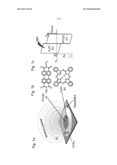
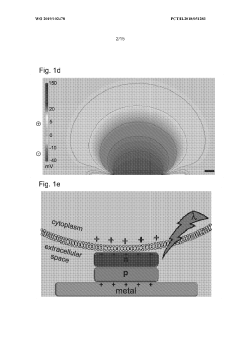
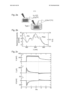
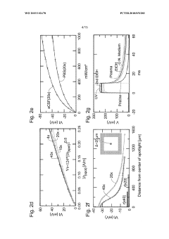
Device and method for neurostimulation
PatentWO2019102478A1
Innovation
- Development of pigment-based devices with organic crystalline semiconductor p-n/n-p heterojunctions that operate as photocapacitors, providing efficient charge photogeneration and capacitive stimulation without Faradaic processes, allowing for direct photoelectrical stimulation of neurons with minimal footprint and no passivation needed.
Fabrication of nanoparticle arrays
PatentWO2005015792A2
Innovation
- The development of methods and apparatus for self-assembling close-packed nanoparticle monolayer arrays, transferring them to substrates, and patterning them, while also removing or exchanging organic molecules to control electrical conductivity and functional properties, using techniques like low-temperature oxidation and molecular exchange processes.
Integration Pathways with Conventional Electronics
The integration of low-power photonic neurons with conventional electronic systems represents a critical frontier in neuromorphic computing. Current integration approaches primarily follow three pathways: hybrid integration, monolithic integration, and 3D heterogeneous integration. Each pathway offers distinct advantages and faces unique challenges in terms of performance, manufacturability, and scalability.
Hybrid integration, the most mature approach, involves separately fabricating photonic and electronic components and then connecting them through wire bonding or flip-chip techniques. This method benefits from the ability to optimize each component independently using established manufacturing processes. Companies like Intel and IBM have demonstrated hybrid neuromorphic systems where electronic circuits handle control functions while photonic neurons perform high-speed computational tasks. However, this approach suffers from increased packaging complexity, higher interconnect losses, and thermal management challenges at interfaces.
Monolithic integration aims to fabricate both photonic and electronic components on the same substrate. Silicon photonics platforms have emerged as promising candidates, leveraging CMOS-compatible processes to integrate photonic neurons directly with electronic control circuitry. Recent advances in silicon-compatible phase-change materials and electro-optic polymers have enabled the development of photonic neurons that can be fabricated alongside transistors. This approach significantly reduces interconnect losses and packaging complexity but faces challenges in material compatibility and process integration.
3D heterogeneous integration represents the newest frontier, where photonic and electronic layers are stacked vertically and connected through through-silicon vias (TSVs) or optical vertical interconnects. This approach maximizes integration density while allowing each layer to be optimized independently. Research groups at MIT and Stanford have demonstrated early prototypes of 3D-integrated photonic neural networks with electronic control layers, achieving significant improvements in energy efficiency and computational density.
The roadmap for integration must address several key challenges. First, thermal management becomes increasingly critical as photonic and electronic components operate in close proximity with different thermal requirements. Second, standardization of interfaces between photonic and electronic domains remains underdeveloped, hindering interoperability. Third, testing methodologies for integrated photonic-electronic systems require significant advancement to ensure reliability at scale.
Looking forward, emerging integration technologies such as photonic interposers and silicon photonic integrated circuits (PICs) with embedded non-volatile photonic memory elements show promise for enabling more seamless integration. Additionally, the development of specialized electronic driver circuits optimized for photonic neuron operation represents an important research direction that could significantly improve overall system efficiency.
Sustainability Impact of Photonic Neural Technologies
The integration of photonic neural technologies into computing systems represents a significant advancement in sustainable computing paradigms. These technologies leverage light-based processing to dramatically reduce energy consumption compared to traditional electronic systems. Current estimates suggest that photonic neural networks can achieve energy efficiency improvements of 10-100x over their electronic counterparts, with theoretical limits potentially reaching 1000x in specialized applications. This energy reduction directly translates to decreased carbon emissions from data centers and computing infrastructure, which currently account for approximately 2% of global electricity consumption.
Material selection for photonic neurons plays a crucial role in their sustainability profile. Silicon photonics, the most mature platform, offers compatibility with existing semiconductor manufacturing infrastructure, reducing the need for new production facilities. Alternative materials such as lithium niobate, chalcogenide glasses, and organic electro-optic polymers present varying environmental footprints. Recent lifecycle assessments indicate that silicon photonic systems generate 30-45% less carbon during manufacturing compared to equivalent electronic systems, primarily due to reduced material complexity and processing steps.
The longevity of photonic neural components further enhances their sustainability credentials. With minimal moving parts and reduced heat generation, photonic systems typically demonstrate extended operational lifespans, estimated at 1.5-2x that of electronic equivalents. This durability reduces electronic waste generation, addressing a growing environmental concern as global e-waste volumes exceed 50 million metric tons annually.
Water conservation represents another significant sustainability advantage. Conventional electronic chip manufacturing requires substantial water resources for cooling and processing. Photonic neural technologies, operating at lower temperatures, can reduce cooling requirements by 40-60%, translating to proportional water savings in manufacturing and operation phases.
Resource efficiency extends to rare earth and critical materials usage. While some specialized photonic components require materials like indium or gallium, ongoing research focuses on developing alternatives using more abundant elements. Current photonic designs have achieved 25-35% reductions in critical material requirements compared to electronic neural implementations with equivalent computational capabilities.
The scalability of photonic neural technologies presents additional sustainability benefits through computational density improvements. Higher integration densities enable more processing power per unit area, reducing the physical footprint of computing infrastructure. This spatial efficiency could potentially reduce land use requirements for data centers by 15-25% when fully implemented, contributing to reduced habitat disruption and urban sprawl associated with expanding digital infrastructure.
Unlock deeper insights with Patsnap Eureka Quick Research — get a full tech report to explore trends and direct your research. Try now!
Generate Your Research Report Instantly with AI Agent
Supercharge your innovation with Patsnap Eureka AI Agent Platform!