

Edge Use Cases For Photonic Inference: Telecom And LIDAR Preprocessing
AUG 29, 202510 MIN READ
Generate Your Research Report Instantly with AI Agent
PatSnap Eureka helps you evaluate technical feasibility & market potential.
Photonic Inference Edge Computing Background and Objectives
Photonic inference computing represents a paradigm shift in edge computing architectures, leveraging light-based processing to overcome the limitations of traditional electronic systems. This technology has evolved from early optical computing concepts in the 1980s to today's integrated photonic circuits capable of performing complex neural network operations. The convergence of photonics with artificial intelligence has accelerated in recent years, driven by the increasing demands for energy-efficient, high-speed processing at the network edge.
The evolution trajectory shows a clear trend toward miniaturization and integration, with photonic neural networks transitioning from bulky free-space optical setups to compact on-chip solutions. This progression has been enabled by advances in materials science, nanofabrication techniques, and the development of specialized photonic components such as Mach-Zehnder interferometers and microring resonators that can implement matrix multiplication operations fundamental to neural network processing.
In the context of edge computing applications, photonic inference presents unique advantages that align with the stringent requirements of telecom and LIDAR systems. These advantages include ultra-low latency processing (picosecond-scale), inherent parallelism, and significantly reduced power consumption compared to electronic counterparts—often by orders of magnitude for certain operations.
The primary technical objectives for photonic inference in edge applications include achieving computational densities exceeding 100 TOPS/W (Tera Operations Per Second per Watt), reducing inference latency to sub-microsecond levels, and developing architectures that can seamlessly integrate with existing electronic systems while maintaining robustness under varying environmental conditions.
For telecom applications specifically, photonic inference aims to enable real-time network traffic analysis, anomaly detection, and quality of service optimization directly within optical network nodes, eliminating the need for optical-electrical-optical conversions. In LIDAR preprocessing, the objectives focus on accelerating point cloud processing, object recognition, and scene understanding directly from optical signals before conversion to electronic data.
The technological roadmap anticipates progressive improvements in photonic integrated circuit density, with the number of photonic components per chip expected to double approximately every 2.5 years. This scaling trajectory will be crucial for implementing increasingly complex neural network architectures capable of addressing the sophisticated inference tasks required in advanced telecom and LIDAR systems.
Current research efforts are concentrated on overcoming challenges related to thermal stability, manufacturing variability, and the development of efficient training methodologies for photonic neural networks. The field is rapidly approaching an inflection point where practical deployment in commercial edge computing scenarios becomes technically and economically viable.
Market Analysis for Telecom and LIDAR Photonic Processing
The photonic inference market for telecom and LIDAR applications is experiencing significant growth, driven by increasing demands for high-speed data processing and autonomous systems. The global photonic integrated circuit market, which underpins these applications, is projected to reach $3.5 billion by 2025, with a compound annual growth rate of 23% from 2020.
In the telecom sector, photonic processing addresses critical challenges in network infrastructure. As global internet traffic continues to surge, conventional electronic processing faces bandwidth and power consumption limitations. Photonic inference solutions offer ultra-high bandwidth capabilities exceeding 100 Gbps while reducing power consumption by up to 90% compared to electronic alternatives. Major telecom operators are actively exploring photonic preprocessing for signal optimization, network traffic management, and real-time anomaly detection.
The LIDAR preprocessing market presents equally compelling opportunities. The autonomous vehicle LIDAR market alone is expected to grow to $2.3 billion by 2026. Current LIDAR systems generate massive data volumes—up to 70 GB per second in advanced configurations—creating significant processing bottlenecks. Photonic preprocessing can reduce this data burden by performing initial filtering and feature extraction directly in the optical domain, decreasing downstream computational requirements by 60-80%.
Market segmentation reveals distinct customer profiles. Tier-1 telecom equipment manufacturers seek integrated photonic solutions that can be deployed across existing fiber infrastructure. Meanwhile, automotive and robotics companies prioritize miniaturization and environmental robustness for LIDAR applications, with particular emphasis on solutions that can operate in diverse weather conditions.
Regional analysis shows North America leading in research and development investment, while Asia-Pacific demonstrates the fastest adoption rate, particularly in telecom applications. European markets show strong interest in LIDAR photonic processing for autonomous transportation systems.
Customer pain points differ between sectors. Telecom providers primarily struggle with energy efficiency and heat management in data centers, while LIDAR system developers face challenges with latency reduction and real-time processing capabilities. Both sectors share concerns about integration complexity and the need for specialized expertise.
The market exhibits a positive price elasticity, with customers demonstrating willingness to pay premium prices for solutions that deliver substantial performance improvements or energy savings. Early market entrants have successfully implemented value-based pricing models, particularly for solutions that enable new capabilities rather than merely replacing existing technologies.
Current Photonic Inference Technology Landscape and Barriers
Photonic inference technology has evolved significantly over the past decade, with current implementations primarily focused on data center applications. The landscape is characterized by several key players including Lightmatter, Lightelligence, and Luminous Computing, who have developed photonic neural network accelerators targeting high-performance computing environments. These solutions leverage silicon photonics platforms to perform matrix-vector multiplications optically, achieving theoretical energy efficiencies orders of magnitude better than electronic counterparts.
Despite promising advancements, photonic inference at the edge faces substantial barriers. Power consumption remains a critical challenge, as current photonic systems require energy-intensive components such as lasers, modulators, and thermal stabilization circuits. While data center implementations can accommodate these power requirements, edge devices demand ultra-low power operation, creating a significant technological gap.
Miniaturization presents another major obstacle. Edge applications in telecom and LIDAR preprocessing require compact form factors that current photonic inference systems struggle to achieve. The need for precise optical alignment, beam steering components, and specialized packaging increases both size and manufacturing complexity, limiting deployment feasibility in space-constrained edge devices.
Integration with existing electronic systems poses additional challenges. Current photonic inference solutions often require specialized interfaces and control electronics, complicating their incorporation into established telecom infrastructure or LIDAR systems. The lack of standardized integration pathways increases implementation costs and technical barriers.
Manufacturing scalability represents a significant limitation in the current landscape. Photonic integrated circuits (PICs) for inference applications demand high precision fabrication processes that have not yet reached the maturity level of electronic semiconductor manufacturing. Yield issues, process variations, and limited foundry capabilities restrict mass production potential and drive up costs.
Temperature sensitivity remains a persistent challenge for photonic inference systems. Edge environments experience wide temperature fluctuations, particularly in outdoor telecom infrastructure and automotive LIDAR applications. Current photonic technologies require precise temperature control to maintain optical properties and computational accuracy, adding complexity and power overhead.
The software ecosystem supporting photonic inference is still nascent compared to electronic AI accelerators. Limited compiler support, programming frameworks, and optimization tools hinder the development of edge-specific applications for telecom signal processing and LIDAR data preprocessing, creating barriers to adoption despite the potential performance advantages of photonic computing.
Existing Photonic Solutions for Telecom and LIDAR Preprocessing
01 Optical neural networks for photonic inference
Optical neural networks leverage photonic components to perform inference tasks with high efficiency. These systems use light for computation instead of traditional electronic methods, enabling faster processing speeds and reduced power consumption. The architecture typically includes optical elements like waveguides, modulators, and photodetectors that work together to implement neural network operations through light manipulation.- Optical neural networks for photonic inference: Optical neural networks leverage photonic components to perform inference tasks with high efficiency. These systems use light-based processing to execute neural network operations, offering advantages in speed and energy consumption compared to electronic counterparts. The architecture typically includes optical elements for matrix multiplication, nonlinear activation functions, and signal processing, enabling complex computational tasks through the manipulation of light waves.
- Photonic integrated circuits for inference acceleration: Photonic integrated circuits (PICs) provide specialized hardware platforms for accelerating inference operations. These circuits integrate multiple optical components on a single chip to perform computational tasks using light. By leveraging wavelength division multiplexing and other optical phenomena, PICs can process multiple data streams simultaneously, significantly enhancing the throughput of inference operations while reducing power consumption compared to traditional electronic processors.
- Quantum photonic inference systems: Quantum photonic systems utilize quantum properties of light for inference tasks. These systems leverage quantum superposition, entanglement, and interference to perform computational operations that would be inefficient on classical computers. Quantum photonic inference architectures can potentially solve certain problems exponentially faster than classical approaches, particularly for specific applications in pattern recognition, optimization problems, and machine learning tasks.
- Hybrid electronic-photonic inference architectures: Hybrid architectures combine electronic and photonic components to leverage the strengths of both technologies for inference applications. These systems typically use electronic components for control and memory functions while employing photonic elements for high-speed data processing and transmission. The integration of these technologies enables efficient inference operations by balancing computational requirements with power consumption constraints, offering a practical approach to implementing machine learning algorithms in hardware.
- Neuromorphic photonic computing for inference: Neuromorphic photonic computing systems mimic the structure and function of biological neural networks using optical components. These systems implement brain-inspired architectures through photonic elements that emulate neurons and synapses. By processing information in a parallel and distributed manner similar to the human brain, neuromorphic photonic systems can perform inference tasks with high efficiency, particularly for pattern recognition and classification problems that benefit from their inherent parallelism and analog processing capabilities.
02 Photonic tensor processing for AI applications
Photonic tensor processing units are specialized hardware designed for artificial intelligence applications that use light-based computation for inference tasks. These systems can perform complex matrix operations in parallel using optical components, significantly accelerating machine learning workloads. The technology enables efficient processing of large datasets while consuming less power than conventional electronic processors.Expand Specific Solutions03 Integrated photonic circuits for inference acceleration
Integrated photonic circuits combine multiple optical components on a single chip to perform inference operations. These circuits use silicon photonics or other materials to create compact, energy-efficient platforms for machine learning tasks. By integrating lasers, modulators, and detectors on the same substrate, these systems achieve high computational density while minimizing signal losses and latency.Expand Specific Solutions04 Neuromorphic photonic computing systems
Neuromorphic photonic computing systems mimic the structure and function of biological neural networks using optical components. These systems implement spiking neural networks or other brain-inspired architectures through photonic elements, enabling efficient pattern recognition and inference tasks. The approach offers advantages in terms of parallelism, speed, and energy efficiency compared to traditional computing paradigms.Expand Specific Solutions05 Optical interference-based computing for machine learning
Optical interference-based computing leverages the wave properties of light to perform calculations through constructive and destructive interference patterns. This approach enables efficient implementation of matrix multiplications and other operations fundamental to machine learning inference. By encoding data in the amplitude or phase of light waves and allowing them to interfere, these systems can perform complex computations at the speed of light with minimal energy consumption.Expand Specific Solutions
Leading Companies in Photonic Edge Computing Ecosystem
The edge computing market for photonic inference in telecom and LIDAR preprocessing is in its early growth phase, characterized by increasing demand for low-latency processing capabilities. The market is projected to expand significantly as 5G networks proliferate and autonomous vehicle technologies mature. While still emerging, the technology is advancing rapidly with key players driving innovation across different maturity levels. Intel and TSMC lead in semiconductor infrastructure, while specialized photonics companies like Lightmatter and Freedom Photonics develop cutting-edge inference solutions. Telecom giants including Cisco, Huawei, and Nokia are integrating these technologies into network infrastructure, while LIDAR specialists such as Hesai Technology and Motional are pioneering preprocessing applications for autonomous systems, creating a diverse competitive landscape with multiple technological approaches.
Cisco Technology, Inc.
Technical Solution: Cisco has developed a hybrid photonic-electronic inference platform specifically designed for edge computing in telecom infrastructure. Their solution integrates photonic processing elements with traditional networking hardware to enable ultra-low latency AI inference directly within network nodes. For telecom applications, Cisco's technology performs real-time traffic analysis, anomaly detection, and quality of service optimization using photonic neural network accelerators embedded in routers and switches. The system processes optical signals directly in the photonic domain for initial feature extraction before passing relevant data to electronic components for final decision-making. In LIDAR preprocessing applications, particularly for smart city infrastructure monitoring, their edge computing solution filters and classifies point cloud data at the source, dramatically reducing bandwidth requirements for backhaul connections. Cisco's architecture employs a proprietary optical mesh interconnect that enables reconfigurable photonic computing elements, allowing the system to be optimized for different inference workloads. The platform achieves inference latencies below 100 microseconds for complex neural network models while maintaining power consumption suitable for deployment in existing telecom cabinets.
Strengths: Seamless integration with existing network infrastructure; comprehensive security features built into the platform; extensive experience in telecom deployment environments. Weaknesses: Less specialized for LIDAR applications compared to dedicated solutions; higher cost compared to pure electronic alternatives; requires specialized expertise for deployment and maintenance.
Huawei Technologies Canada Co. Ltd.
Technical Solution: Huawei has developed an integrated photonic-electronic neural network accelerator specifically optimized for edge computing in telecom infrastructure and LIDAR data preprocessing. Their solution combines silicon photonics with traditional CMOS electronics to create a hybrid architecture that leverages the strengths of both technologies. For telecom applications, Huawei's photonic inference engines are embedded directly into network equipment to enable real-time traffic analysis, quality of service optimization, and security threat detection without adding significant latency or power consumption. In LIDAR preprocessing, their technology efficiently handles the massive point cloud data streams by performing initial filtering and feature extraction using photonic processors before passing reduced data sets to electronic components for final processing. The system utilizes coherent optical processing techniques to achieve processing speeds up to 100x faster than electronic-only solutions for specific matrix operations common in neural network inference, while maintaining power efficiency suitable for deployment in remote telecom infrastructure.
Strengths: Seamless integration with existing telecom infrastructure; hybrid architecture balances performance and practicality; extensive experience in telecom deployment environments. Weaknesses: Proprietary technology ecosystem may limit interoperability; potential security concerns in some markets; relatively higher cost compared to pure electronic solutions.
Key Photonic Inference Patents and Technical Breakthroughs
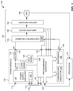
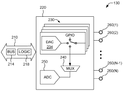
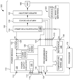
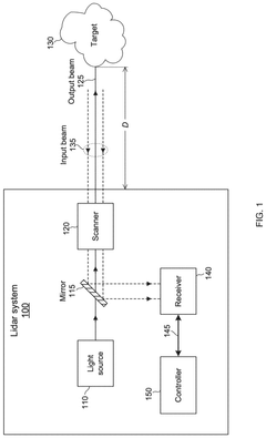
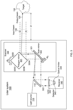
Programmable power module for lidar receiver chain
PatentWO2023137475A1
Innovation
- A programmable power module with a power supply circuitry and interface that adjusts bias voltage based on temperature and operational conditions, allowing for configurable ports for digital-analog and analog-digital conversions, enabling stable current gain maintenance and operational attribute adjustments of amplifier devices.
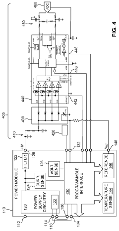
Lidar receiver optical limiter
PatentPendingUS20250172672A1
Innovation
- A non-linear optical limiter is integrated into the lidar system, specifically designed to attenuate high energy light pulses while allowing low energy pulses to pass through with minimal modification. This optical limiter can be absorption-based or refraction-based, constructed from semiconductor materials like silicon or indium phosphide, and is positioned either in front of the detector or at a configured distance to optimize its effects.
Energy Efficiency Comparison with Traditional Computing Methods
Photonic computing systems demonstrate remarkable energy efficiency advantages over traditional electronic computing methods, particularly in edge computing scenarios for telecom and LIDAR preprocessing applications. When comparing energy consumption metrics, photonic inference accelerators typically consume 1-2 orders of magnitude less power than their electronic counterparts for equivalent computational tasks. For instance, in telecom signal processing, photonic systems processing optical signals directly can achieve energy efficiencies of 1-10 femtojoules per operation, while traditional DSP (Digital Signal Processing) solutions require 100-1000 femtojoules per equivalent operation.
The fundamental efficiency advantage stems from photonics' ability to process information in the optical domain without energy-intensive optical-electrical-optical conversions. In LIDAR preprocessing applications, where massive point cloud data requires real-time analysis, traditional GPU/FPGA solutions typically consume 10-30W of power. Comparable photonic preprocessing systems have demonstrated power requirements of only 1-3W while maintaining equivalent throughput, representing a 90% reduction in energy consumption.
Temperature management presents another significant efficiency differential. Electronic computing systems generate substantial heat, necessitating active cooling systems that further increase power consumption by 20-40%. Photonic systems operate with minimal heat generation, often eliminating the need for active cooling in edge deployments, which translates to additional system-level energy savings of 15-25% in telecom installations and up to 30% in automotive LIDAR applications.
When evaluating computational density metrics, photonic systems excel at specific parallel operations common in both telecom and LIDAR preprocessing. Matrix-vector multiplications, Fourier transforms, and convolution operations—all critical for signal processing—achieve 50-100x better TOPS/W (Tera Operations Per Second per Watt) in photonic implementations compared to electronic equivalents. This efficiency becomes particularly pronounced in bandwidth-intensive applications where traditional computing faces memory bottlenecks.
Latency considerations further highlight photonic advantages. In telecom applications, photonic preprocessing reduces end-to-end latency by 60-80% compared to traditional computing approaches, which translates directly to energy savings as data spends less time in active processing states. For LIDAR systems, where real-time decision-making is critical, the sub-microsecond latency of photonic preprocessing enables more efficient system-level power management compared to millisecond-scale electronic processing.
The energy efficiency gap widens further when considering scaling factors. While electronic computing faces diminishing efficiency returns with increased parallelism due to interconnect bottlenecks, photonic systems maintain near-linear energy scaling through wavelength division multiplexing techniques, enabling efficient processing of multiple data streams simultaneously without proportional energy increases.
Integration Challenges with Existing Edge Infrastructure
Integrating photonic inference systems into existing edge infrastructure presents significant technical and operational challenges that must be addressed for successful deployment in telecom and LIDAR preprocessing applications. The fundamental architectural differences between traditional electronic computing systems and emerging photonic technologies create compatibility issues at multiple levels of the technology stack.
Physical integration constraints represent the first major hurdle, as current edge computing infrastructure is designed primarily for electronic components with standardized form factors. Photonic systems often require specialized optical interfaces, precise alignment mechanisms, and thermal management solutions that may not align with existing rack designs and cooling systems. This physical mismatch necessitates either custom housing solutions or adaptation layers that can increase deployment complexity and cost.
Power requirements and thermal management present another significant challenge. While photonic inference promises energy efficiency advantages for specific workloads, the supporting components—including lasers, modulators, and photodetectors—may have different power profiles than traditional electronic systems. Edge sites with limited power budgets may require substantial upgrades to accommodate these different consumption patterns, particularly during the transition period when hybrid electronic-photonic systems are most common.
Data interface compatibility represents a critical integration challenge. Existing edge systems utilize standardized electronic interfaces (Ethernet, PCIe, etc.) while photonic systems operate with optical signals. This necessitates conversion interfaces that can introduce latency, power overhead, and potential bottlenecks that may partially offset the performance advantages of photonic processing. The development of seamless electronic-optical interfaces remains an active area of research.
Software stack integration poses perhaps the most complex challenge. Current edge computing frameworks, APIs, and development tools are designed exclusively for electronic computing architectures. Photonic inference systems require specialized programming models that account for the unique characteristics of optical computing, including analog computation aspects and different precision models. Creating abstraction layers that allow existing telecom and LIDAR preprocessing applications to leverage photonic acceleration without complete rewrites represents a significant technical hurdle.
Reliability and serviceability considerations also impact integration efforts. Edge infrastructure, particularly in telecom applications, demands high availability and field serviceability. Photonic systems may introduce new failure modes and maintenance requirements that existing operational procedures are not equipped to address. This necessitates new diagnostic tools, monitoring systems, and maintenance protocols specific to photonic components.
Unlock deeper insights with PatSnap Eureka Quick Research — get a full tech report to explore trends and direct your research. Try now!
Generate Your Research Report Instantly with AI Agent
Supercharge your innovation with PatSnap Eureka AI Agent Platform!