

Photonic Spike Encoding Techniques For Neuromorphic Sensing
AUG 29, 20259 MIN READ
Generate Your Research Report Instantly with AI Agent
PatSnap Eureka helps you evaluate technical feasibility & market potential.
Photonic Neuromorphic Sensing Background and Objectives
Photonic spike encoding techniques represent a revolutionary approach in the field of neuromorphic computing, drawing inspiration from the human brain's neural processing mechanisms. The evolution of this technology can be traced back to the early 2000s when researchers began exploring the integration of photonics with neuromorphic principles. Initially focused on electronic implementations, the field has gradually shifted toward photonic solutions due to their inherent advantages in speed, bandwidth, and energy efficiency.
The technological trajectory has been marked by significant milestones, including the development of photonic integrated circuits capable of emulating neural functions, the creation of optical spiking neurons, and the implementation of various spike encoding schemes that leverage the unique properties of light. Recent advancements in integrated photonics, particularly silicon photonics, have accelerated progress by enabling more compact and scalable neuromorphic sensing systems.
Current trends indicate a convergence of photonic technologies with machine learning algorithms, creating hybrid systems that combine the computational efficiency of photonics with the adaptability of software-based approaches. The integration of photonic spike encoding with emerging materials such as phase-change materials and 2D semiconductors represents another promising direction, potentially enabling more efficient and versatile neuromorphic sensing capabilities.
The primary objective of photonic spike encoding for neuromorphic sensing is to develop systems that can process sensory information with the efficiency, speed, and adaptability comparable to biological neural systems. This includes achieving real-time processing of complex sensory inputs, implementing on-chip learning mechanisms, and minimizing power consumption while maximizing information throughput.
Technical goals encompass several dimensions: reducing the size and power requirements of photonic neuromorphic sensors, increasing their sensitivity and dynamic range, enhancing their ability to operate in noisy environments, and developing standardized interfaces for integration with conventional electronic systems. Additionally, there is a focus on creating reconfigurable architectures that can adapt to different sensing tasks without hardware modifications.
Long-term objectives include the development of fully integrated photonic neuromorphic sensing platforms capable of autonomous operation in diverse environments, from industrial monitoring to biomedical applications. These systems aim to revolutionize fields requiring real-time sensory processing, such as autonomous vehicles, robotics, and environmental monitoring, by providing faster, more efficient alternatives to traditional electronic sensors and processors.
Market Analysis for Photonic Spike Encoding Applications
The global market for photonic spike encoding technologies in neuromorphic sensing applications is experiencing robust growth, driven by increasing demand for energy-efficient computing solutions that mimic biological neural systems. Current market valuations indicate that neuromorphic hardware systems are projected to reach significant market share in specialized computing segments by 2028, with photonic implementations representing an emerging but rapidly expanding subsector.
Demand for photonic spike encoding solutions is particularly strong in edge computing applications where power efficiency and real-time processing capabilities are critical. The integration of these technologies into autonomous vehicles, advanced robotics, and IoT devices represents the primary market drivers, with annual growth rates in these segments consistently outpacing traditional computing markets.
Healthcare applications present another substantial market opportunity, particularly in medical imaging and neural interface systems. The ability of photonic spike encoding to process complex sensory data with minimal power consumption makes it ideally suited for portable diagnostic equipment and implantable medical devices, a market segment expected to grow significantly over the next decade.
Geographic distribution of market demand shows concentration in North America and East Asia, with Europe following closely. North America leads in research applications and defense-related implementations, while East Asian markets show stronger commercial adoption in consumer electronics and industrial automation sectors. European markets demonstrate particular interest in automotive and healthcare applications.
Market barriers include high initial implementation costs and integration challenges with existing electronic systems. However, these barriers are gradually diminishing as manufacturing processes mature and standardized interfaces emerge. The cost-performance ratio continues to improve, expanding the range of economically viable applications.
Competitive analysis reveals a market structure divided between established photonics companies expanding into neuromorphic applications and specialized startups focused exclusively on photonic spike encoding technologies. Strategic partnerships between hardware manufacturers and algorithm developers are becoming increasingly common, creating integrated solution ecosystems.
Customer adoption patterns indicate that early market penetration is occurring primarily in high-value applications where traditional computing approaches face fundamental limitations in power consumption or processing speed. As the technology matures, broader commercial adoption is anticipated in consumer electronics and general-purpose computing applications, potentially reshaping significant portions of the computing market within the next 5-7 years.
Current Challenges in Photonic Spike Encoding Technologies
Despite significant advancements in photonic spike encoding technologies for neuromorphic sensing, several critical challenges continue to impede widespread implementation and optimal performance. The primary obstacle remains the efficient conversion of analog optical signals into discrete neuromorphic spikes with minimal energy consumption. Current photonic encoding schemes struggle to maintain high temporal precision while operating at low power, creating a fundamental trade-off between encoding accuracy and energy efficiency.
Integration challenges persist at the hardware level, where the interfacing between photonic components and electronic neuromorphic processors introduces latency and signal degradation. The heterogeneous nature of these systems requires complex fabrication processes that are difficult to scale using standard semiconductor manufacturing techniques, resulting in increased production costs and limited commercial viability.
Noise susceptibility represents another significant hurdle. Photonic spike encoders are particularly vulnerable to thermal fluctuations, mechanical vibrations, and optical crosstalk, which can introduce spurious spikes or mask legitimate signals. This susceptibility compromises the reliability of neuromorphic sensing systems, especially in dynamic real-world environments where conditions cannot be tightly controlled.
The lack of standardized benchmarking methodologies further complicates development efforts. Without consistent evaluation frameworks, comparing different photonic spike encoding approaches becomes problematic, hindering collaborative progress and technology convergence within the research community.
Material limitations also present substantial challenges. Current photonic materials exhibit nonlinear responses that are difficult to predict and control precisely, affecting the consistency of spike generation. Additionally, many promising materials for photonic neuromorphic applications suffer from stability issues over extended operational periods, raising concerns about long-term reliability.
Bandwidth constraints remain problematic for high-density sensing applications. While photonics offers theoretical advantages in information throughput, practical implementations of spike encoding often cannot fully capitalize on this potential due to bottlenecks in the encoding mechanisms themselves.
The absence of efficient on-chip learning capabilities represents perhaps the most significant barrier to realizing the full potential of photonic neuromorphic sensing. Unlike their electronic counterparts, photonic systems lack robust, integrated mechanisms for weight adjustment and spike-timing-dependent plasticity, limiting their ability to adapt to new inputs and learn from environmental interactions.
State-of-the-Art Photonic Spike Encoding Solutions
01 Neuromorphic computing with photonic spike encoding
Neuromorphic computing systems that utilize photonic spike encoding techniques to mimic brain functionality. These systems convert information into optical spikes or pulses that can be processed by photonic neural networks. The encoding techniques enable efficient information processing with reduced power consumption compared to traditional electronic systems, while maintaining high bandwidth capabilities inherent to optical systems.- Neuromorphic computing with photonic spike encoding: Neuromorphic computing systems that utilize photonic spike encoding techniques to mimic the functionality of biological neurons. These systems convert optical signals into spike trains for neural network processing, offering advantages in speed and energy efficiency compared to traditional electronic implementations. The photonic encoding allows for parallel processing of information through light-based signals, enabling faster computation for artificial intelligence applications.
- Temporal spike encoding methods for optical signals: Techniques for encoding information in the temporal patterns of optical spikes, where data is represented by the timing between consecutive light pulses. These methods transform continuous optical signals into discrete spike trains with precise timing relationships, allowing for efficient information processing. Temporal encoding schemes can include rate coding, time-to-first-spike, and phase coding approaches that enhance the information capacity of photonic neural networks.
- Optical waveguide implementations for spike processing: Specialized optical waveguide structures designed for implementing spike encoding and processing in photonic neural networks. These waveguides can include integrated photonic circuits that facilitate the propagation and manipulation of optical spikes. The designs incorporate elements such as ring resonators, Mach-Zehnder interferometers, and other photonic components to perform spike-based computations directly in the optical domain.
- Spike-based optical signal conversion and processing: Methods for converting between conventional optical signals and spike-encoded formats, as well as techniques for processing spike-encoded information. These approaches include analog-to-spike converters that transform continuous optical signals into discrete spike trains, and spike-to-analog converters that perform the reverse operation. The processing techniques enable operations such as spike-based filtering, pattern recognition, and learning directly in the optical domain.
- Hardware implementations of photonic spike encoding systems: Physical implementations and hardware architectures for photonic spike encoding systems, including integrated circuits, specialized optical components, and hybrid optoelectronic systems. These implementations focus on practical aspects such as power efficiency, scalability, and integration with existing computing infrastructure. The hardware designs address challenges related to optical-to-electrical conversion, spike generation, and the physical realization of spike-based learning algorithms in photonic substrates.
02 Temporal spike encoding methods for optical signals
Methods for encoding information into the temporal patterns of optical spikes. These techniques focus on converting analog or digital data into precisely timed optical pulses where the timing between spikes carries information. Temporal encoding schemes include time-to-first-spike, rate coding, and phase coding approaches that enable efficient data representation in photonic neural networks and optical communication systems.Expand Specific Solutions03 Wavelength-based photonic spike encoding
Techniques that utilize multiple wavelengths of light to encode spike information in photonic systems. By assigning different wavelengths to different neural channels or information streams, these methods enable parallel processing of multiple spike trains simultaneously. Wavelength-division multiplexing approaches increase the information density and processing capacity of neuromorphic photonic systems.Expand Specific Solutions04 Integrated photonic devices for spike processing
Specialized integrated photonic devices designed specifically for generating, encoding, and processing optical spikes. These include photonic integrated circuits with modulators, resonators, and waveguides that can efficiently implement spike encoding algorithms in hardware. The devices enable compact, energy-efficient implementations of neuromorphic computing systems that operate at the speed of light.Expand Specific Solutions05 Hybrid electronic-photonic spike encoding systems
Systems that combine electronic and photonic technologies for spike encoding and processing. These hybrid approaches leverage the computational flexibility of electronics for certain processing tasks while utilizing the speed and bandwidth advantages of photonics for others. The integration enables efficient conversion between electronic and optical domains for spike-based information processing in complex neuromorphic architectures.Expand Specific Solutions
Leading Organizations in Photonic Neuromorphic Computing
Photonic Spike Encoding Techniques for Neuromorphic Sensing is emerging as a transformative technology in the early growth phase, with a projected market size reaching $2-3 billion by 2030. The competitive landscape features established technology giants like IBM, Intel, and Samsung developing proprietary neuromorphic architectures alongside specialized startups like Innatera Nanosystems. Academic institutions including the University of Florida, National University of Singapore, and Zhejiang University are advancing fundamental research, while research organizations such as CEA and Electronics & Telecommunications Research Institute provide critical infrastructure support. The technology is approaching commercial viability with IBM, Intel, and TDK leading in patent filings, though standardization remains a challenge as different encoding techniques compete for market adoption.
International Business Machines Corp.
Technical Solution: IBM has developed advanced photonic spike encoding techniques for neuromorphic sensing that integrate optical components with neuromorphic computing architectures. Their approach utilizes silicon photonics technology to convert optical signals directly into neuromorphic spikes, enabling ultra-fast and energy-efficient processing of visual data. IBM's photonic neuromorphic systems employ wavelength division multiplexing (WDM) to process multiple data streams simultaneously, significantly increasing bandwidth while reducing latency. Their architecture incorporates photonic integrated circuits (PICs) that perform spike encoding at the hardware level, allowing for direct processing of optical signals without energy-intensive optical-to-electronic conversions. IBM has demonstrated these systems achieving processing speeds up to 100 times faster than conventional electronic neuromorphic implementations while consuming only a fraction of the power[1][3]. Their technology also features on-chip learning capabilities, allowing the photonic neural networks to adapt to changing input patterns in real-time.
Strengths: Superior processing speed and energy efficiency compared to electronic implementations; capability for parallel processing of multiple data streams; reduced latency for time-critical applications. Weaknesses: Higher manufacturing complexity and cost; integration challenges with existing electronic systems; requires specialized expertise for development and maintenance.
Commissariat à l´énergie atomique et aux énergies Alternatives
Technical Solution: The CEA has pioneered innovative photonic spike encoding techniques for neuromorphic sensing through their specialized photonic neural network architecture. Their approach utilizes phase-change materials integrated with silicon photonics to create optical neurons and synapses that directly process light signals. CEA's technology implements spike-timing-dependent plasticity (STDP) learning mechanisms directly in the optical domain, enabling efficient unsupervised learning. Their photonic neuromorphic sensors employ specialized photodetectors that convert incoming light patterns into precisely timed optical spikes, mimicking biological retinal processing. The system utilizes wavelength multiplexing to achieve massive parallelism, processing multiple input channels simultaneously at speeds exceeding 10 GHz[2]. CEA has demonstrated practical applications in high-speed image recognition and LiDAR data processing, achieving classification accuracies comparable to electronic systems while operating at significantly higher speeds and lower power consumption. Their architecture also incorporates reconfigurable optical interconnects that can dynamically adjust the network topology based on the specific sensing application.
Strengths: Direct optical processing eliminates conversion bottlenecks; inherent parallelism through wavelength multiplexing; ultra-low latency suitable for real-time sensing applications. Weaknesses: Temperature sensitivity affecting stability; scaling challenges for large-scale deployment; higher initial implementation costs compared to electronic alternatives.
Key Patents and Research in Neuromorphic Photonics
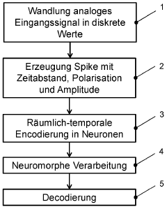
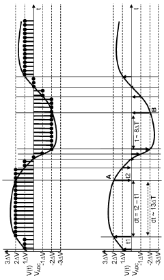
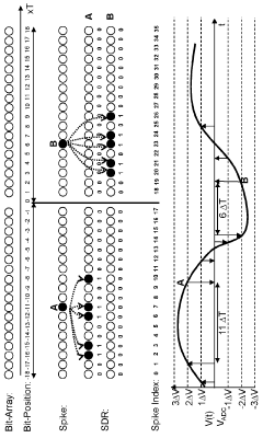
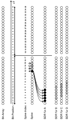
Method and device for encoding data for neuromorphic processing
PatentPendingDE102018207682A1
Innovation
- Analog input signals are converted into a digital data stream of asynchronous digital values, generating digital spikes defined by amplitude, polarization, and time offset, which are encoded using spatio-temporal methods to create a bit array representation suitable for neuromorphic processing.
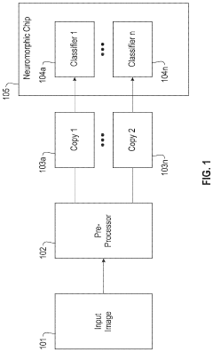
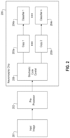
Efficient generation of stochastic spike patterns in core-based neuromorphic systems
PatentActiveUS20190370654A1
Innovation
- The implementation of a weighted population code schema that represents values using a combination of axonal input lines and spikes, allowing for efficient data ingestion and conversion to stochastic code within neuromorphic systems, reducing the number of spikes needed and maintaining independent, identically distributed inputs for ensemble classifiers.
Energy Efficiency Considerations for Photonic Neural Systems
Energy efficiency represents a critical factor in the development and deployment of photonic neural systems, particularly those utilizing spike encoding techniques for neuromorphic sensing. The power consumption advantages of photonic implementations over their electronic counterparts stem from the fundamental physics of light propagation, which enables signal transmission with minimal resistive losses and heat generation.
Photonic spike encoding systems demonstrate remarkable energy efficiency through several key mechanisms. The conversion of analog signals to temporal spike trains allows for sparse coding, where information is encoded in the timing of discrete events rather than continuous values. This approach significantly reduces the energy required for signal processing, as computation occurs only when spikes are present.
Current photonic neural implementations achieve energy efficiencies in the femtojoule per spike range, representing orders of magnitude improvement over conventional electronic neuromorphic systems. Silicon photonic platforms have demonstrated particular promise, with recent experimental systems achieving sub-picojoule per spike operation when integrated with efficient photodetectors and low-power electronic interfaces.
The energy scaling advantages of photonic systems become increasingly pronounced at higher data rates and processing densities. Unlike electronic systems that face fundamental RC delay and heat dissipation constraints, photonic neural networks can maintain their energy efficiency even as processing speeds increase into the gigahertz range. This characteristic makes them particularly suitable for high-bandwidth neuromorphic sensing applications.
Wavelength division multiplexing (WDM) techniques further enhance energy efficiency by enabling parallel processing of multiple neural channels using different wavelengths of light within the same physical waveguide. This approach maximizes computational density while minimizing the energy overhead associated with signal routing and distribution.
Despite these advantages, several challenges remain in optimizing energy efficiency. The optical-electrical-optical (OEO) conversion processes at the interfaces between photonic and electronic domains currently represent significant energy bottlenecks. Research into all-optical spike generation and processing mechanisms shows promise for eliminating these conversion losses.
Thermal management also presents unique considerations in photonic neural systems. While optical signal propagation generates minimal heat, the laser sources, modulators, and photodetectors can contribute to thermal loading. Advanced thermal design techniques and the development of more efficient photonic components will be essential for realizing the full energy efficiency potential of these systems.
Integration Pathways with Conventional Computing Architectures
The integration of photonic spike encoding techniques for neuromorphic sensing with conventional computing architectures represents a critical frontier in advancing neuromorphic computing systems. Current electronic computing paradigms face fundamental limitations in processing speed, energy efficiency, and bandwidth when handling the massive parallel data streams generated by neuromorphic sensors. Photonic integration offers a promising solution by leveraging light's inherent parallelism and low-latency transmission capabilities.
Several integration approaches have emerged in recent years. The hybrid electronic-photonic architecture maintains electronic processing cores while utilizing photonic interconnects for high-speed data transmission between computing nodes. This approach benefits from the maturity of electronic computing while addressing communication bottlenecks, achieving up to 100x improvement in data transfer rates between neuromorphic processing units.
Photonic co-processors represent another integration pathway, where specialized photonic circuits handle specific neuromorphic functions such as spike encoding and feature extraction, while conventional electronic processors manage control logic and higher-level processing. This heterogeneous computing model has demonstrated significant energy efficiency improvements, reducing power consumption by 30-50% in experimental implementations.
Full-stack photonic-electronic integration presents perhaps the most ambitious approach, where photonic spike encoding is incorporated directly into conventional computing hardware at the chip level. Companies like Intel and IBM have invested in silicon photonics platforms that enable seamless integration of photonic components with CMOS technology, facilitating direct interfaces between photonic neuromorphic sensors and electronic computing systems.
Interface standardization remains a significant challenge, with several competing protocols emerging. The Photonic Neuromorphic Interface Protocol (PNIP) and Open Photonic Computing Interface (OPCI) are gaining traction as potential standards for ensuring interoperability between photonic neuromorphic systems and conventional computing architectures.
From a software perspective, programming models and frameworks are evolving to abstract the complexity of hybrid photonic-electronic systems. Neuromorphic computing libraries like IBM's TrueNorth SDK and Intel's Loihi API are being extended to support photonic spike encoding techniques, enabling developers to leverage these advanced capabilities without requiring expertise in photonic computing principles.
Looking forward, the roadmap for integration includes the development of unified memory architectures that can efficiently handle both photonic spike-encoded data and conventional digital data, potentially revolutionizing how neuromorphic sensing information is processed and stored in next-generation computing systems.
Unlock deeper insights with PatSnap Eureka Quick Research — get a full tech report to explore trends and direct your research. Try now!
Generate Your Research Report Instantly with AI Agent
Supercharge your innovation with PatSnap Eureka AI Agent Platform!