Thermal Management For High-Density Photonic Compute Modules
AUG 29, 20259 MIN READ
Generate Your Research Report Instantly with AI Agent
Patsnap Eureka helps you evaluate technical feasibility & market potential.
Photonic Computing Thermal Challenges and Objectives
Photonic computing represents a paradigm shift in computational architecture, leveraging light instead of electrons to process information. This technology promises significant advantages in processing speed, bandwidth, and energy efficiency compared to traditional electronic computing systems. However, as photonic computing modules increase in density and complexity, thermal management emerges as a critical challenge that must be addressed to realize the full potential of this technology.
The evolution of photonic computing has been marked by progressive miniaturization and integration of optical components, leading to higher component densities and consequently increased thermal loads. Historical developments in silicon photonics have enabled the integration of multiple optical functions onto a single chip, but this integration has exacerbated thermal challenges. The heat generated by lasers, modulators, and other active components can significantly impact the performance and reliability of photonic systems.
Temperature fluctuations affect the refractive index of optical materials, leading to wavelength shifts and performance degradation in photonic devices. For instance, a temperature change of just 1°C can cause wavelength shifts of approximately 0.1nm in silicon waveguides, potentially disrupting the precise wavelength control required for many photonic computing applications. This sensitivity necessitates sophisticated thermal management strategies to maintain stable operating conditions.
Current technical objectives in photonic computing thermal management focus on several key areas. First, developing efficient heat dissipation mechanisms that can handle the concentrated thermal loads of high-density photonic modules without compromising optical performance. Second, designing thermally-aware photonic architectures that minimize heat generation while maximizing computational capabilities. Third, implementing active thermal control systems capable of maintaining precise temperature stability across photonic components.
The industry aims to achieve thermal management solutions that can maintain temperature variations below ±0.5°C across photonic computing modules, ensuring wavelength stability and consistent performance. Additionally, there is a push toward reducing the energy overhead of cooling systems, targeting cooling power consumption below 20% of the total system power budget, compared to current figures that often exceed 40%.
Looking forward, the technical roadmap for photonic computing thermal management includes the development of integrated microfluidic cooling channels, thermoelectric cooling elements embedded directly within photonic integrated circuits, and advanced thermal interface materials with enhanced thermal conductivity. These innovations will be crucial in enabling the next generation of high-density photonic compute modules that can deliver unprecedented computational power while maintaining thermal stability.
Market Analysis for High-Density Photonic Compute Solutions
The global market for high-density photonic compute solutions is experiencing robust growth, driven by increasing demands for high-performance computing in data centers, telecommunications, artificial intelligence, and quantum computing applications. Current market valuations indicate that the photonic computing sector is projected to grow at a compound annual growth rate of 30% through 2030, with thermal management solutions representing approximately 15% of this expanding market.
The demand for photonic compute modules is primarily fueled by their advantages in processing speed, energy efficiency, and bandwidth capabilities compared to traditional electronic systems. Organizations across various sectors are increasingly adopting these solutions to handle complex computational tasks while reducing energy consumption. Financial institutions leverage photonic computing for high-frequency trading algorithms, while research institutions implement these systems for complex simulations and modeling.
Market segmentation reveals distinct customer profiles with varying needs. Hyperscale cloud providers prioritize scalability and integration with existing infrastructure, while telecommunications companies focus on reliability and compatibility with network architectures. Research institutions and universities value customization options and cutting-edge performance metrics, even at premium price points.
Regional analysis shows North America currently leading market adoption, accounting for approximately 40% of global market share, followed by Asia-Pacific at 35% and Europe at 20%. China, Japan, and South Korea are making significant investments in domestic photonic computing capabilities, potentially shifting the market landscape within the next five years.
Thermal management specifically represents a critical market differentiator, with customers increasingly prioritizing solutions that address heat dissipation challenges. Market research indicates that 78% of potential adopters cite thermal management concerns as a primary consideration in purchasing decisions, highlighting the commercial importance of innovations in this area.
The competitive landscape features established semiconductor manufacturers expanding into photonics, specialized photonic startups securing significant venture capital funding, and research institutions commercializing breakthrough technologies. Strategic partnerships between thermal solution providers and photonic chip manufacturers are becoming increasingly common, creating new market opportunities and integrated product offerings.
Price sensitivity varies significantly by market segment, with enterprise customers demonstrating willingness to pay premium prices for solutions that deliver demonstrable performance improvements and operational cost reductions. The total cost of ownership, including energy consumption and cooling requirements, has emerged as a key decision factor, creating market opportunities for thermally efficient designs that command higher initial prices but deliver long-term operational savings.
Current Thermal Management Limitations in Photonics
Current thermal management approaches in photonic computing face significant limitations as integration densities continue to increase. Traditional cooling methods such as forced air convection have reached their practical limits, with heat fluxes in high-density photonic modules now exceeding 100-150 W/cm². This thermal ceiling creates a fundamental bottleneck for further miniaturization and performance scaling of photonic compute architectures.
The temperature sensitivity of photonic components presents a particularly challenging constraint. Laser sources, modulators, and detectors typically require operating temperatures below 85°C to maintain wavelength stability and prevent performance degradation. Even minor temperature fluctuations of 1-2°C can cause wavelength shifts that significantly impact system performance, especially in wavelength division multiplexing (WDM) applications where channel spacing is extremely tight.
Thermal crosstalk between adjacent photonic components represents another critical limitation. As component density increases, heat generated by one element affects the performance of neighboring devices, creating complex thermal management challenges that conventional cooling approaches struggle to address. This thermal interdependence limits the practical packing density achievable in current photonic integrated circuits.
The interface between electronic and photonic components compounds these challenges. Hybrid integration of CMOS electronics with photonic elements creates thermal hotspots at transition points, with heat dissipation requirements that differ significantly between the two domains. Current thermal management solutions often optimize for one domain at the expense of the other, resulting in suboptimal overall system performance.
Power consumption for cooling systems themselves has become a significant limitation. In data center environments, cooling overhead can consume 30-40% of total system power, severely impacting the energy efficiency advantages that photonic computing promises to deliver. This cooling penalty undermines one of the primary motivations for adopting photonic computing architectures.
Material limitations further constrain thermal management options. While materials like silicon dioxide provide excellent optical properties, their poor thermal conductivity (approximately 1.4 W/m·K) creates thermal bottlenecks. Alternative materials with better thermal properties often compromise optical performance, forcing difficult engineering tradeoffs that limit overall system capabilities.
Finally, current thermal simulation and modeling tools lack the integrated electro-optical-thermal capabilities needed to accurately predict behavior in complex photonic systems. This modeling gap forces designers to implement excessive thermal safety margins, resulting in suboptimal designs that underutilize the theoretical performance potential of photonic computing architectures.
State-of-the-Art Cooling Techniques for Photonic Modules
01 Liquid cooling systems for photonic compute modules
Liquid cooling systems are employed for efficient thermal management of photonic compute modules. These systems utilize coolants to absorb and transfer heat away from heat-generating components. The liquid cooling approach offers superior thermal conductivity compared to air cooling, allowing for more effective temperature control in high-density photonic computing environments. Advanced implementations include closed-loop systems with heat exchangers and specialized coolant formulations optimized for optical computing components.- Liquid cooling systems for photonic compute modules: Liquid cooling systems are employed for thermal management of photonic compute modules. These systems utilize coolants to efficiently dissipate heat generated during operation. The liquid cooling approach offers superior thermal conductivity compared to air cooling, allowing for more effective temperature control in high-density photonic computing environments. Advanced implementations include closed-loop systems with heat exchangers and specialized coolant formulations optimized for optical computing components.
- Heat sink designs for optical computing components: Specialized heat sink designs are developed specifically for optical computing components to manage thermal loads. These heat sinks feature optimized geometries and materials to maximize heat dissipation from photonic integrated circuits and related components. Advanced designs incorporate micro-channel structures, phase-change materials, and thermally conductive interfaces to efficiently transfer heat away from sensitive optical elements while maintaining precise operating temperatures required for photonic computing.
- Power management techniques for thermal control: Power management techniques are implemented to control thermal conditions in photonic compute modules. These approaches include dynamic voltage and frequency scaling, selective component activation, and workload distribution to prevent hotspots. Advanced power management systems monitor thermal conditions in real-time and adjust computing resources accordingly to maintain optimal operating temperatures while preserving performance. These techniques help extend component lifespan and improve overall system reliability in photonic computing environments.
- Thermal interface materials for photonic components: Specialized thermal interface materials are developed to enhance heat transfer between photonic components and cooling systems. These materials feature high thermal conductivity while maintaining optical compatibility with sensitive photonic elements. Advanced formulations include phase-change materials, metal-infused polymers, and nanostructured composites designed to minimize thermal resistance at component interfaces. These materials help maintain optimal operating temperatures for photonic integrated circuits and related optical computing elements.
- Integrated thermal monitoring and management systems: Integrated systems for thermal monitoring and management are implemented in photonic compute modules. These systems incorporate temperature sensors, control algorithms, and cooling mechanisms working together to maintain optimal thermal conditions. Advanced implementations feature machine learning capabilities to predict thermal behavior and proactively adjust cooling parameters. The integrated approach enables real-time thermal management across complex photonic computing architectures, ensuring reliable operation while optimizing energy efficiency.
02 Heat dissipation structures for optical components
Specialized heat dissipation structures are designed for optical components in photonic compute modules. These include heat sinks, thermal spreaders, and thermally conductive interfaces that efficiently transfer heat away from sensitive optical elements. The structures are engineered to maintain optimal operating temperatures for photonic integrated circuits, waveguides, and other optical components while minimizing thermal gradients that could affect optical performance. Materials with high thermal conductivity and specialized geometries are employed to maximize heat transfer efficiency.Expand Specific Solutions03 Thermal management control systems for photonic computing
Advanced control systems are implemented to dynamically manage thermal conditions in photonic compute modules. These systems utilize temperature sensors, feedback loops, and predictive algorithms to monitor and regulate thermal parameters. The control architecture can adjust cooling resources based on computational load, ambient conditions, and thermal thresholds of optical components. Some implementations incorporate machine learning techniques to optimize thermal management strategies over time, balancing cooling efficiency with power consumption while maintaining optical signal integrity.Expand Specific Solutions04 Integration of thermal management with photonic circuit design
Thermal management considerations are integrated directly into the design of photonic integrated circuits and compute modules. This approach involves strategic placement of heat-generating components, thermal isolation of temperature-sensitive optical elements, and incorporation of thermal pathways within the photonic circuit layout. Design methodologies include thermal simulation during the development phase to identify and mitigate potential hotspots. The integration enables more compact photonic compute modules while maintaining thermal stability for consistent optical performance.Expand Specific Solutions05 Energy-efficient cooling techniques for photonic systems
Energy-efficient cooling techniques are developed specifically for photonic computing systems to reduce overall power consumption while maintaining optimal thermal conditions. These techniques include phase-change materials, passive cooling designs, and thermally adaptive structures that respond to temperature variations. Some approaches leverage ambient cooling when possible and implement intelligent power management to reduce heat generation at the source. The focus is on achieving the necessary thermal management with minimal energy expenditure, enhancing the overall efficiency of photonic compute modules.Expand Specific Solutions
Leading Companies in Photonic Computing Thermal Management
The thermal management market for high-density photonic compute modules is in its growth phase, with increasing demand driven by data center expansion and AI applications. The market is projected to reach significant scale as photonic computing advances toward commercialization. Leading semiconductor companies like Intel, NVIDIA, AMD, and Qualcomm are investing heavily in this space, while specialized cooling technology providers such as JETCOOL Technologies are developing innovative microjet cooling solutions. Established telecommunications players including ZTE, InnoLight, and Sumitomo Electric are contributing optical integration expertise. The technology is approaching commercial maturity with several companies demonstrating working prototypes, though challenges remain in scaling thermal solutions for next-generation photonic compute densities.
JETCOOL Technologies, Inc.
Technical Solution: JETCOOL has developed a revolutionary microconvective cooling technology specifically designed for high-density photonic compute modules. Their solution employs direct-to-chip liquid cooling with microjet arrays that target hotspots with precision cooling. The technology utilizes an array of high-velocity, laminar fluid jets that impinge directly onto the heat-generating components, creating numerous microscale convective cells that efficiently remove heat from photonic integrated circuits (PICs). This approach achieves thermal resistance values as low as 0.05°C/W, enabling cooling capacities exceeding 1000 W/cm² while maintaining junction temperatures below critical thresholds. The system incorporates a closed-loop cooling circuit with specialized non-conductive, optically transparent coolants that are compatible with photonic components and ensure signal integrity in optical pathways[1][2].
Strengths: Superior thermal performance with extremely low thermal resistance; enables significantly higher power densities than conventional cooling methods; precision cooling of hotspots without affecting optical pathways; compact form factor suitable for dense integration. Weaknesses: Requires specialized coolant infrastructure; higher initial implementation costs compared to passive solutions; potential reliability concerns with fluid systems in optical environments.
Intel Corp.
Technical Solution: Intel has pioneered a silicon photonics thermal management solution that addresses the unique challenges of high-density photonic compute modules. Their approach integrates thermal management directly into the silicon photonics manufacturing process, creating monolithically integrated thermal pathways. Intel's solution employs embedded thermoelectric coolers (TECs) strategically positioned near critical photonic components such as lasers and modulators that require precise temperature control. These micro-TECs provide localized active cooling with temperature stability within ±0.1°C. The system is complemented by a network of diamond-filled thermal vias with thermal conductivity exceeding 1500 W/m·K that efficiently channel heat away from photonic components to the package substrate. Intel's thermal architecture incorporates a hierarchical cooling approach where passive elements handle background thermal loads while active elements address dynamic hotspots. Their solution also features integrated thermal sensors and a closed-loop control system that maintains optimal operating temperatures across varying workloads, ensuring wavelength stability in dense wavelength division multiplexing (DWDM) applications[5][6].
Strengths: Highly integrated approach with thermal management built into silicon photonics platform; exceptional temperature stability for wavelength-sensitive components; mature manufacturing process enabling high-volume production; comprehensive thermal modeling capabilities. Weaknesses: Higher manufacturing complexity and cost; power consumption overhead from active cooling elements; limited flexibility for thermal redesigns after fabrication; potential reliability issues with embedded TECs over extended operation.
Critical Patents in Photonic Thermal Dissipation
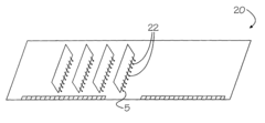
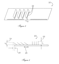
High density, high frequency memory chip modules having thermal management structures
PatentInactiveUS20030068920A1
Innovation
- The development of an ultra-high density, three-dimensional electronic circuit package with demountable connectors and integrated thermal management structures, including ground planes and heat-spreading fins, allows for reduced inductance, controlled impedance, and efficient heat dissipation, enabling high-speed and high-frequency operations with easy rework and testing capabilities.
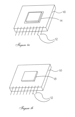
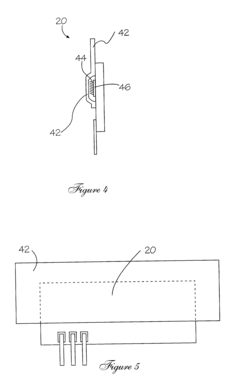
Thermal interposer for thermal management of semiconductor devices
PatentInactiveUS20050280162A1
Innovation
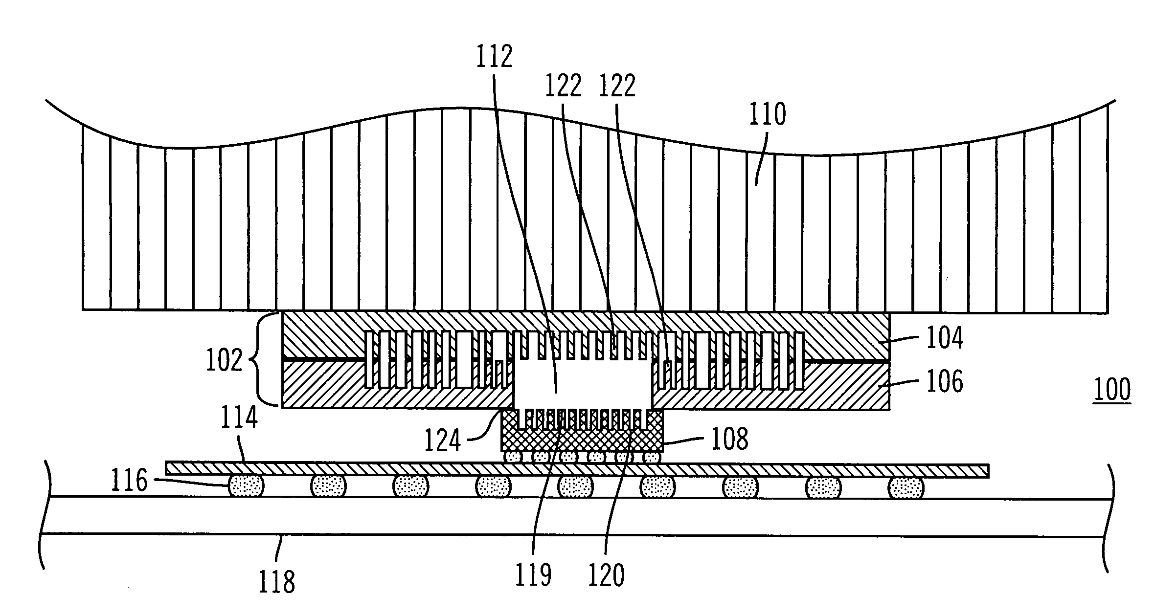
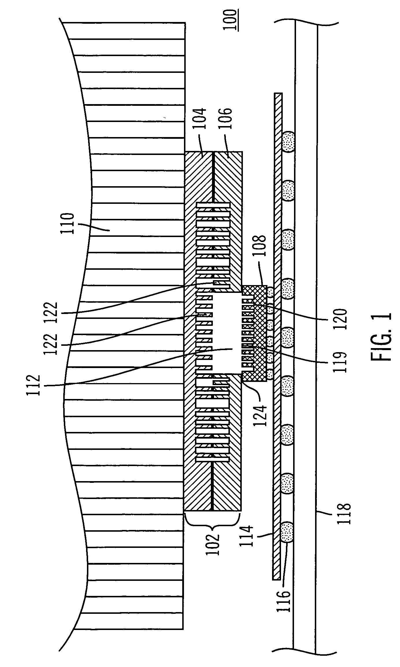
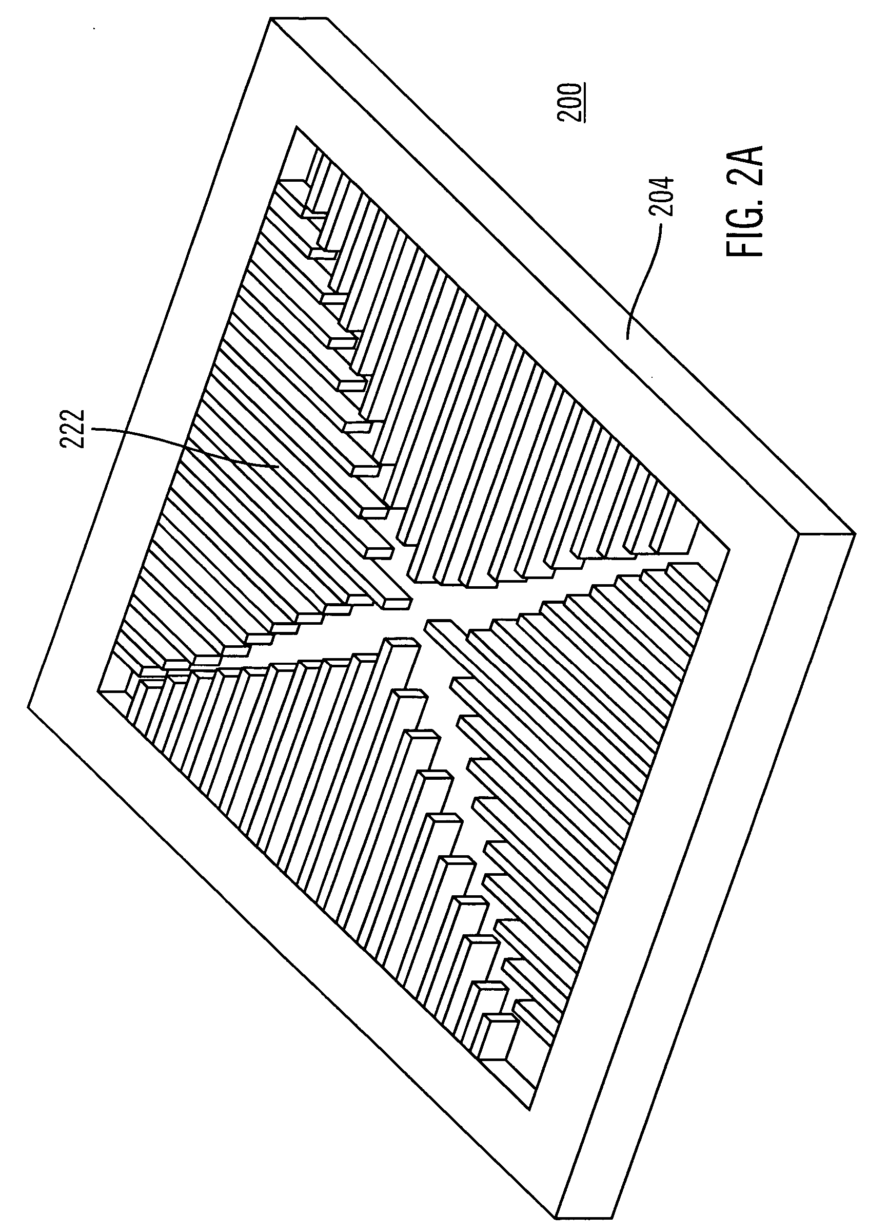
- The development of thermal interposers with vapor chambers formed by hermetically bonding plates of materials with matching thermal expansion coefficients to the semiconductor device, incorporating wick structures like grooves and graphite foam for efficient heat transfer and reduced thermal resistance.
Material Innovations for Thermal Efficiency
Material innovations represent a critical frontier in addressing thermal challenges for high-density photonic compute modules. Recent advancements in thermal interface materials (TIMs) have yielded compounds with thermal conductivity exceeding 25 W/m·K, significantly outperforming traditional silicone-based materials. These next-generation TIMs incorporate graphene, carbon nanotubes, and metallic nanoparticles to create highly efficient thermal pathways between heat-generating components and cooling systems.
Diamond-based materials have emerged as particularly promising candidates for thermal management applications. Chemical vapor deposition (CVD) diamond substrates offer thermal conductivity values approaching 2000 W/m·K, approximately five times that of copper. While cost remains a barrier to widespread adoption, thin diamond films are increasingly viable for targeted deployment in critical thermal pathways.
Phase change materials (PCMs) represent another innovative approach, absorbing excess heat during computational peaks through solid-to-liquid transitions. Advanced PCMs specifically engineered for photonic applications demonstrate melting points between 45-65°C, aligning with optimal operating temperatures for photonic integrated circuits. These materials provide effective thermal buffering during transient workloads, preventing damaging temperature spikes.
Ceramic matrix composites (CMCs) combining silicon carbide with aluminum nitride have demonstrated exceptional thermal performance while maintaining electrical insulation properties. These composites achieve thermal conductivity values of 170-220 W/m·K while exhibiting coefficient of thermal expansion values closely matched to silicon photonics substrates, minimizing thermomechanical stress during thermal cycling.
Aerogel-based insulation materials represent a complementary approach, providing strategic thermal isolation between components operating at different temperature regimes. Silica aerogels with thermal conductivity below 0.02 W/m·K enable precise thermal zoning within densely packed photonic modules, preventing thermal crosstalk between sensitive components.
Metal matrix composites (MMCs) incorporating copper or aluminum matrices with high-conductivity reinforcements like diamond particles or carbon fibers offer tailored thermal management solutions. These materials combine the processability of metals with enhanced thermal performance, achieving conductivity values 30-50% higher than pure metals while maintaining mechanical robustness required for manufacturing processes.
Emerging two-dimensional materials including hexagonal boron nitride (h-BN) and molybdenum disulfide (MoS2) demonstrate anisotropic thermal properties that can be leveraged for directional heat transfer in layered photonic architectures. These materials enable thermal engineers to create preferential heat flow paths, directing waste heat away from temperature-sensitive components toward designated cooling interfaces.
Energy Consumption and Sustainability Considerations
The energy consumption of high-density photonic compute modules represents a significant operational concern that directly impacts both cost efficiency and environmental sustainability. These advanced computing systems, while offering superior performance in terms of data processing capabilities, typically consume substantial amounts of energy, with a significant portion being converted to heat. Current photonic computing architectures demonstrate energy consumption rates ranging from 10-100 pJ/bit, which, though more efficient than traditional electronic systems, still present challenges when scaled to high-density configurations.
Thermal management solutions themselves contribute to the overall energy footprint of these systems. Active cooling mechanisms such as liquid cooling systems and thermoelectric coolers can consume between 20-40% of the total system power budget. This additional energy overhead must be factored into comprehensive efficiency calculations when evaluating the viability of photonic computing implementations in data centers and high-performance computing environments.
From a sustainability perspective, the environmental impact of photonic compute modules extends beyond operational energy consumption to include manufacturing processes and materials. The production of specialized optical components often involves rare earth elements and energy-intensive fabrication techniques. Life cycle assessments indicate that the embodied energy in photonic components can be 2-3 times higher than conventional electronic counterparts, necessitating longer operational lifespans to achieve net environmental benefits.
Carbon footprint considerations are increasingly driving design decisions in this field. Recent industry analyses suggest that data centers implementing high-density photonic systems could potentially reduce their carbon emissions by 15-30% compared to traditional electronic systems, provided that efficient thermal management strategies are employed. This potential reduction stems primarily from decreased cooling requirements and improved computational efficiency per watt.
Emerging sustainable approaches include the integration of waste heat recovery systems that capture and repurpose thermal energy from photonic modules. These systems can redirect heat for facility warming or convert it to electrical energy through thermoelectric generators, achieving energy recovery rates of 10-25%. Additionally, the development of biodegradable or recyclable photonic materials represents a promising frontier for reducing end-of-life environmental impact.
Regulatory frameworks worldwide are increasingly imposing stricter energy efficiency standards on computing infrastructure. The EU's Ecodesign Directive and similar regulations in North America and Asia are establishing maximum power consumption thresholds that will impact the design and deployment of next-generation photonic computing systems. Compliance with these evolving standards necessitates innovative approaches to thermal management that balance performance requirements with energy efficiency goals.
Unlock deeper insights with Patsnap Eureka Quick Research — get a full tech report to explore trends and direct your research. Try now!
Generate Your Research Report Instantly with AI Agent
Supercharge your innovation with Patsnap Eureka AI Agent Platform!
