ITO Free Electrode: Innovations in Contact Resistance
SEP 28, 202510 MIN READ
Generate Your Research Report Instantly with AI Agent
Patsnap Eureka helps you evaluate technical feasibility & market potential.
ITO-Free Electrode Technology Background and Objectives
Indium Tin Oxide (ITO) has dominated the transparent conductive electrode market for decades due to its excellent combination of optical transparency and electrical conductivity. However, the increasing demand for flexible electronics, rising indium costs, and technical limitations of ITO have driven significant research into alternative materials and technologies. The evolution of transparent electrodes began in the 1950s with the development of ITO, followed by decades of optimization. Recent years have witnessed an acceleration in the development of ITO-free alternatives, responding to both economic and technical imperatives.
The primary objective of ITO-free electrode technology is to overcome the fundamental limitations of traditional ITO electrodes while maintaining or improving performance metrics. These limitations include brittleness that prevents application in flexible devices, high processing temperatures incompatible with many substrates, and the scarcity of indium as a resource. Additionally, ITO exhibits significant contact resistance issues at interfaces with organic materials, limiting efficiency in many optoelectronic applications.
Technical evolution trends indicate a shift toward nanomaterial-based solutions, including metal nanowires, carbon nanotubes, graphene, and conductive polymers. Each alternative offers unique advantages in specific application contexts, with research increasingly focused on hybrid approaches that combine multiple materials to achieve optimal performance characteristics. The field is moving toward solution-processable materials that enable low-cost, large-area manufacturing techniques such as roll-to-roll processing.
The technology goals for next-generation ITO-free electrodes include achieving sheet resistance below 10 ohms/square with optical transparency exceeding 90% in the visible spectrum. Additionally, these materials must demonstrate mechanical flexibility with negligible performance degradation after thousands of bending cycles, compatibility with solution processing at low temperatures (<150°C), and significantly reduced contact resistance at interfaces with organic semiconductors and other functional materials.
Contact resistance represents a particularly critical challenge, as it often dominates device performance limitations in thin-film technologies. Innovations targeting the reduction of contact resistance through interface engineering, work function modification, and novel electrode architectures are expected to yield substantial improvements in device efficiency and reliability. The ultimate goal is to develop electrodes that not only replace ITO but enable entirely new device architectures and applications previously constrained by ITO's limitations.
As global electronics markets continue expanding into wearable, flexible, and large-area applications, the development of cost-effective, high-performance ITO-free electrodes has become strategically important for maintaining technological competitiveness across multiple industries, from consumer electronics to renewable energy.
Market Demand Analysis for Low-Resistance Transparent Electrodes
The transparent electrode market is experiencing significant growth driven by the expanding display and touch panel industries. The global market for transparent conductive films was valued at approximately $5.1 billion in 2022 and is projected to reach $7.8 billion by 2028, growing at a CAGR of 7.3%. This growth is primarily fueled by increasing demand for smartphones, tablets, wearable devices, and large-format displays, all of which require high-performance transparent electrodes.
Indium Tin Oxide (ITO) has traditionally dominated this market, accounting for over 85% of transparent electrode applications. However, several market factors are driving the demand for ITO-free alternatives with lower contact resistance. The rising price and supply constraints of indium, a rare earth metal, have created significant market volatility. Between 2020 and 2022, indium prices fluctuated by more than 40%, creating cost uncertainties for manufacturers.
Consumer electronics manufacturers are increasingly demanding flexible and foldable displays, which ITO cannot adequately support due to its brittle nature. Market research indicates that the flexible display segment is growing at 35% annually, significantly outpacing the overall display market. This shift represents a substantial opportunity for ITO-free electrodes that can maintain low contact resistance while offering mechanical flexibility.
Energy efficiency has become a critical market driver, with manufacturers seeking transparent electrodes that minimize power consumption. Lower contact resistance directly translates to improved energy efficiency, particularly important for battery-powered devices. Market surveys indicate that 78% of smartphone manufacturers consider energy efficiency a top priority in component selection.
The automotive industry represents an emerging high-value market for transparent electrodes, with smart windshields and integrated displays requiring solutions that offer both durability and low resistance. This sector is expected to grow at 25% annually through 2028, creating new application opportunities for advanced electrode technologies.
Regional analysis shows Asia-Pacific dominating manufacturing capacity, accounting for 67% of global production, while North America and Europe lead in research and development of next-generation materials. Chinese manufacturers have significantly increased investment in alternative electrode technologies, with R&D spending in this sector growing by 22% annually since 2020.
The market is increasingly segmenting based on performance requirements, with premium applications willing to pay substantial premiums for electrodes offering superior conductivity, transparency, and flexibility. This trend creates opportunities for innovative ITO-free solutions that can deliver enhanced performance metrics, particularly in contact resistance optimization.
Current Status and Challenges in Contact Resistance Reduction
The global pursuit of ITO-free electrodes has intensified due to indium's scarcity and rising costs, with current contact resistance challenges representing a significant barrier to widespread adoption. Traditional ITO (Indium Tin Oxide) electrodes typically achieve contact resistance values of 10-20 Ω·cm², while emerging ITO-free alternatives struggle to match this performance consistently. This disparity creates a technological bottleneck that limits the commercial viability of otherwise promising alternative materials.
Recent research indicates that interface engineering remains the primary challenge in reducing contact resistance for ITO-free electrodes. The heterojunction formed between alternative transparent conductive materials and active layers often creates energy barriers that impede efficient charge transfer. Materials such as PEDOT:PSS, while offering good transparency and flexibility, still exhibit contact resistance values 30-50% higher than ITO in many applications, particularly affecting device performance under high current densities.
Manufacturing scalability presents another significant challenge. While laboratory-scale demonstrations have shown promising results with carbon nanotubes, graphene, and metal nanowire networks achieving contact resistance values approaching ITO benchmarks, these processes often rely on techniques that are difficult to scale industrially. Vacuum deposition methods for metal-based alternatives like aluminum-doped zinc oxide (AZO) can achieve more consistent results but at higher production costs that offset the material cost advantages.
Environmental stability remains problematic for many ITO alternatives. Silver nanowire networks, despite their excellent conductivity, suffer from oxidation and electromigration under operating conditions, leading to increasing contact resistance over time. Similarly, conductive polymers often demonstrate degradation when exposed to moisture and oxygen, resulting in performance deterioration that particularly affects contact interfaces.
The trade-off between transparency and conductivity continues to challenge researchers. Materials that achieve lower contact resistance often sacrifice optical transparency or require thicker layers that reduce device efficiency. This fundamental materials science challenge has prompted exploration of hybrid structures and composite materials that can optimize both properties simultaneously.
Regional differences in research focus are notable, with East Asian institutions predominantly pursuing metal oxide alternatives, European research centers focusing on carbon-based materials, and North American efforts concentrated on nanomaterial solutions. This geographical distribution of expertise has created knowledge silos that sometimes impede collaborative progress on contact resistance challenges.
Recent breakthroughs in 2022-2023 have demonstrated promising approaches using interface modification layers and doping strategies that have reduced contact resistance in some ITO-free electrodes by up to 40%, suggesting pathways toward competitive performance. However, these solutions often introduce additional processing steps that impact manufacturing complexity and cost structures.
Current Technical Solutions for ITO-Free Electrodes
01 Alternative transparent conductive materials to replace ITO
Various materials are being developed as alternatives to Indium Tin Oxide (ITO) for transparent electrodes with improved contact resistance properties. These alternatives include metal nanowires, conductive polymers, carbon-based materials like graphene, and metal mesh structures. These materials aim to provide comparable or superior conductivity while eliminating the brittleness and high cost associated with ITO.- Alternative transparent conductive materials to replace ITO: Various materials are being developed to replace Indium Tin Oxide (ITO) in electrode applications while maintaining low contact resistance. These alternatives include metal nanowires, conductive polymers, carbon-based materials (graphene, carbon nanotubes), and metal mesh structures. These materials offer advantages such as flexibility, cost-effectiveness, and comparable or improved conductivity compared to traditional ITO electrodes.
- Surface treatment methods to reduce contact resistance: Various surface treatment techniques are employed to reduce contact resistance in ITO-free electrodes. These include plasma treatment, chemical modification, annealing processes, and surface functionalization. These treatments modify the interface properties between the electrode and adjacent layers, removing contaminants and improving charge transfer across interfaces, thereby reducing contact resistance in electronic devices.
- Multilayer electrode structures for improved performance: Multilayer electrode structures are designed to overcome the limitations of single-material electrodes. These structures typically combine different conductive materials in layers to optimize both transparency and conductivity while minimizing contact resistance. Common configurations include metal/metal-oxide bilayers, buffer layer insertions, and gradient composition structures that facilitate better charge transfer at interfaces.
- Novel deposition techniques for ITO-free electrodes: Advanced deposition methods are crucial for creating high-quality ITO-free electrodes with low contact resistance. These techniques include solution processing (spin coating, spray coating), vacuum deposition methods (sputtering, evaporation), printing technologies (inkjet, screen printing), and roll-to-roll processing. Each method offers specific advantages in terms of material compatibility, scalability, and the ability to create uniform films with optimal electrical properties.
- Device-specific electrode optimization strategies: Different electronic devices require specific electrode optimization approaches to minimize contact resistance while maintaining other required properties. For touch panels and displays, the focus is on balancing transparency with conductivity. In solar cells, the emphasis is on work function matching and light management. For flexible electronics, the key considerations include mechanical durability under bending stress while maintaining electrical performance. These device-specific strategies involve tailored material selection and interface engineering.
02 Surface treatment methods to reduce contact resistance
Various surface treatment techniques are employed to reduce the contact resistance of ITO-free electrodes. These include plasma treatment, chemical etching, annealing processes, and surface functionalization with specific compounds. These treatments modify the surface properties of the electrode materials to improve electrical contact with adjacent layers and reduce interface resistance.Expand Specific Solutions03 Multilayer electrode structures for improved conductivity
Multilayer electrode structures are designed to improve conductivity and reduce contact resistance in ITO-free applications. These structures typically combine different conductive materials in layers to optimize both transparency and conductivity. Common approaches include metal/metal-oxide bilayers, conductive polymer composites with metal grids, and sandwich structures with buffer layers to improve interfacial properties.Expand Specific Solutions04 Doping strategies to enhance electrode conductivity
Doping strategies are implemented to enhance the conductivity of ITO-free electrode materials. Various dopants are incorporated into base materials to increase carrier concentration and mobility, thereby reducing contact resistance. Common approaches include metal doping of oxide semiconductors, nitrogen or fluorine doping of carbon-based materials, and ionic additives in conductive polymers to optimize charge transfer properties.Expand Specific Solutions05 Novel manufacturing techniques for low-resistance electrodes
Innovative manufacturing techniques are being developed to create ITO-free electrodes with low contact resistance. These include solution-based processing methods, roll-to-roll fabrication, laser patterning, inkjet printing of conductive materials, and self-assembly approaches. These techniques focus on creating uniform, defect-free electrode structures with optimized interfaces to minimize resistance while enabling cost-effective large-scale production.Expand Specific Solutions
Key Industry Players in Alternative Electrode Technologies
The ITO Free Electrode market is currently in a growth phase, with increasing demand driven by innovations in contact resistance technology. The market size is expanding rapidly as industries seek more efficient and cost-effective alternatives to traditional ITO electrodes. From a technical maturity perspective, companies like Texas Instruments, Samsung Electro-Mechanics, and Toshiba are leading commercial applications, while research institutions such as Zhejiang University and Shenyang Polytechnic University are advancing fundamental innovations. Japanese firms including Murata Manufacturing, TDK, and Shin-Etsu Handotai have established strong positions in materials development, while emerging players like Nanoteco and Changzhou Sixth Element are introducing disruptive technologies focusing on novel materials and manufacturing processes to overcome traditional contact resistance limitations.
Toshiba Corp.
Technical Solution: Toshiba Corporation has developed an innovative ITO-free electrode technology based on carbon nanotube (CNT) networks. Their approach utilizes single-walled carbon nanotubes with controlled chirality and length distributions to create transparent conductive films with sheet resistance of approximately 100-200 ohms/square while maintaining optical transparency above 85%. To address contact resistance challenges, Toshiba has implemented specialized surface functionalization techniques that modify the CNT surfaces with selected chemical groups to optimize charge transfer at electrode interfaces. Their manufacturing process employs solution-based deposition methods combined with laser patterning to create precise electrode geometries. Toshiba has further enhanced this technology by developing hybrid structures that incorporate metallic nanoparticles at CNT junctions, creating localized regions of improved conductivity that significantly reduce overall contact resistance. This approach has been successfully implemented in their display products, particularly for applications requiring mechanical flexibility where traditional ITO electrodes would fail. The company has also developed specialized annealing processes that optimize the CNT network morphology to minimize junction resistance while maintaining optical transparency.
Strengths: Superior mechanical durability compared to ITO, with resistance to repeated bending and flexing; environmentally friendly manufacturing process using non-toxic materials; excellent chemical stability. Weaknesses: Higher sheet resistance compared to metal-based alternatives; more complex manufacturing process requiring precise control of CNT properties; potential for performance variability between production batches.
SAMSUNG ELECTRO MECHANICS CO LTD
Technical Solution: Samsung Electro Mechanics has developed advanced ITO-free electrode technology based on hybrid metal nanowire networks. Their solution utilizes silver nanowires (AgNWs) with diameters of approximately 20-30nm and lengths of 20-30μm, embedded in specialized polymer matrices to create transparent conductive films with sheet resistance as low as 15 ohms/square while maintaining optical transparency above 90%. To address contact resistance challenges, Samsung has implemented proprietary junction engineering techniques that optimize the nanowire-to-nanowire contact points through controlled sintering processes. Their manufacturing approach includes specialized surface treatments that enhance adhesion between the nanowire network and adjacent layers in display or touch sensor structures. Samsung has further refined this technology by incorporating graphene-enhanced contact points at critical interfaces, creating hybrid structures that leverage the benefits of both nanowire conductivity and graphene's exceptional electrical properties. This technology has been implemented in Samsung's flexible OLED displays, enabling reduced power consumption and improved touch responsiveness compared to traditional ITO-based solutions.
Strengths: Exceptional flexibility and stretchability suitable for next-generation flexible electronics; simplified manufacturing process compared to ITO sputtering; excellent performance under mechanical stress with minimal resistance changes. Weaknesses: Long-term stability challenges in harsh environmental conditions; potential for silver migration under high humidity; requires specialized encapsulation to prevent degradation.
Core Innovations in Contact Resistance Optimization
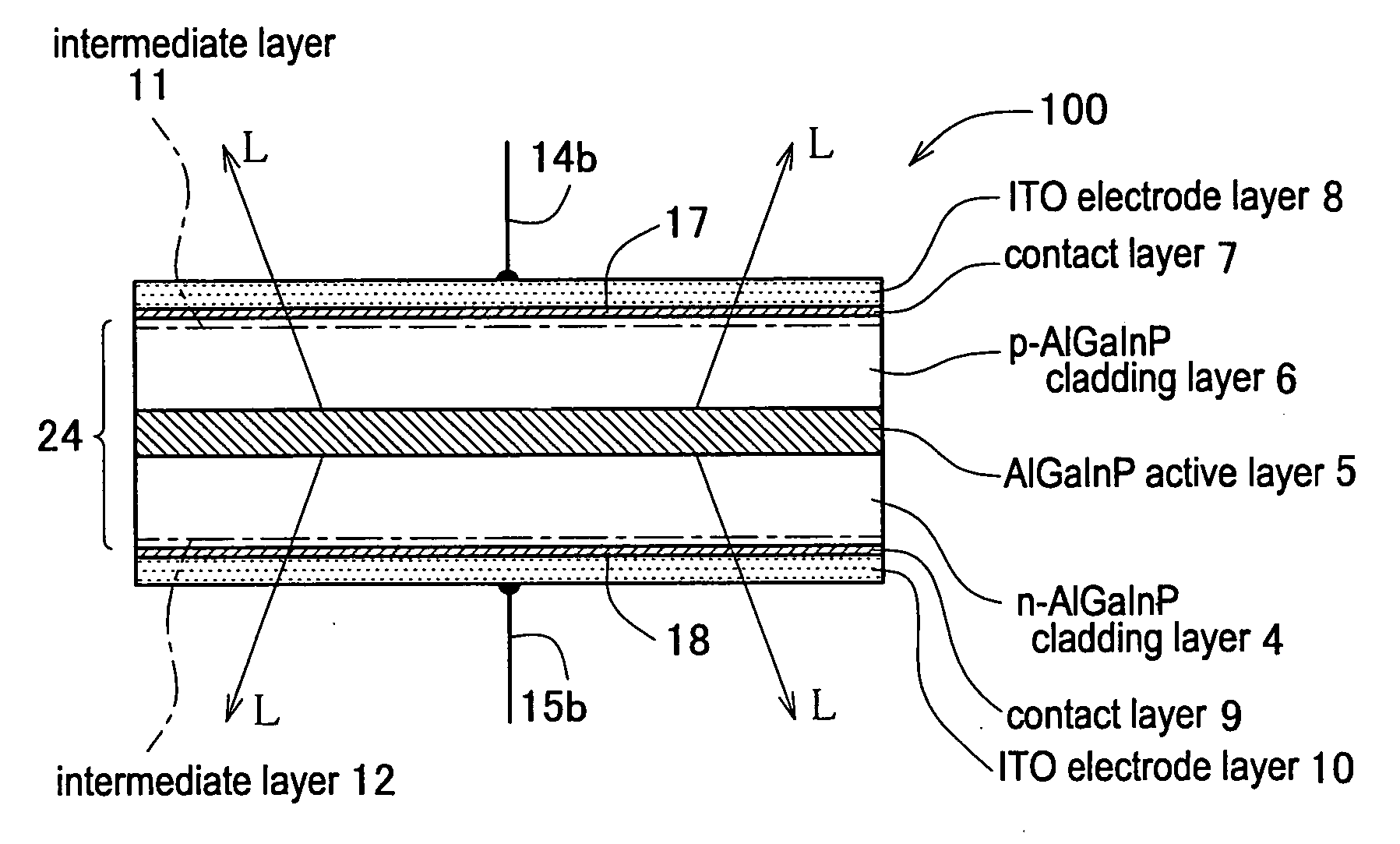
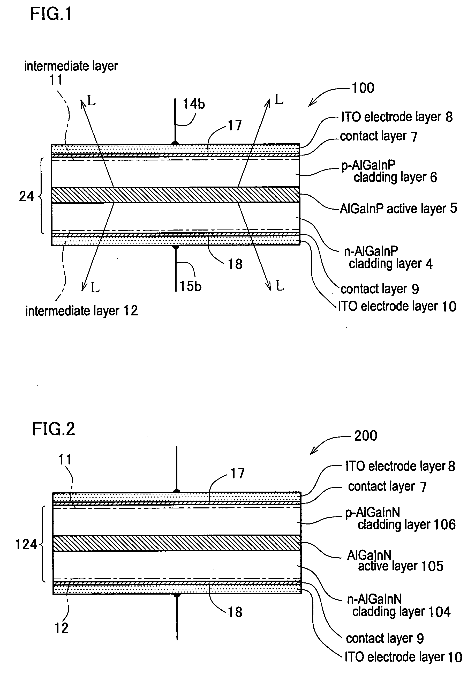
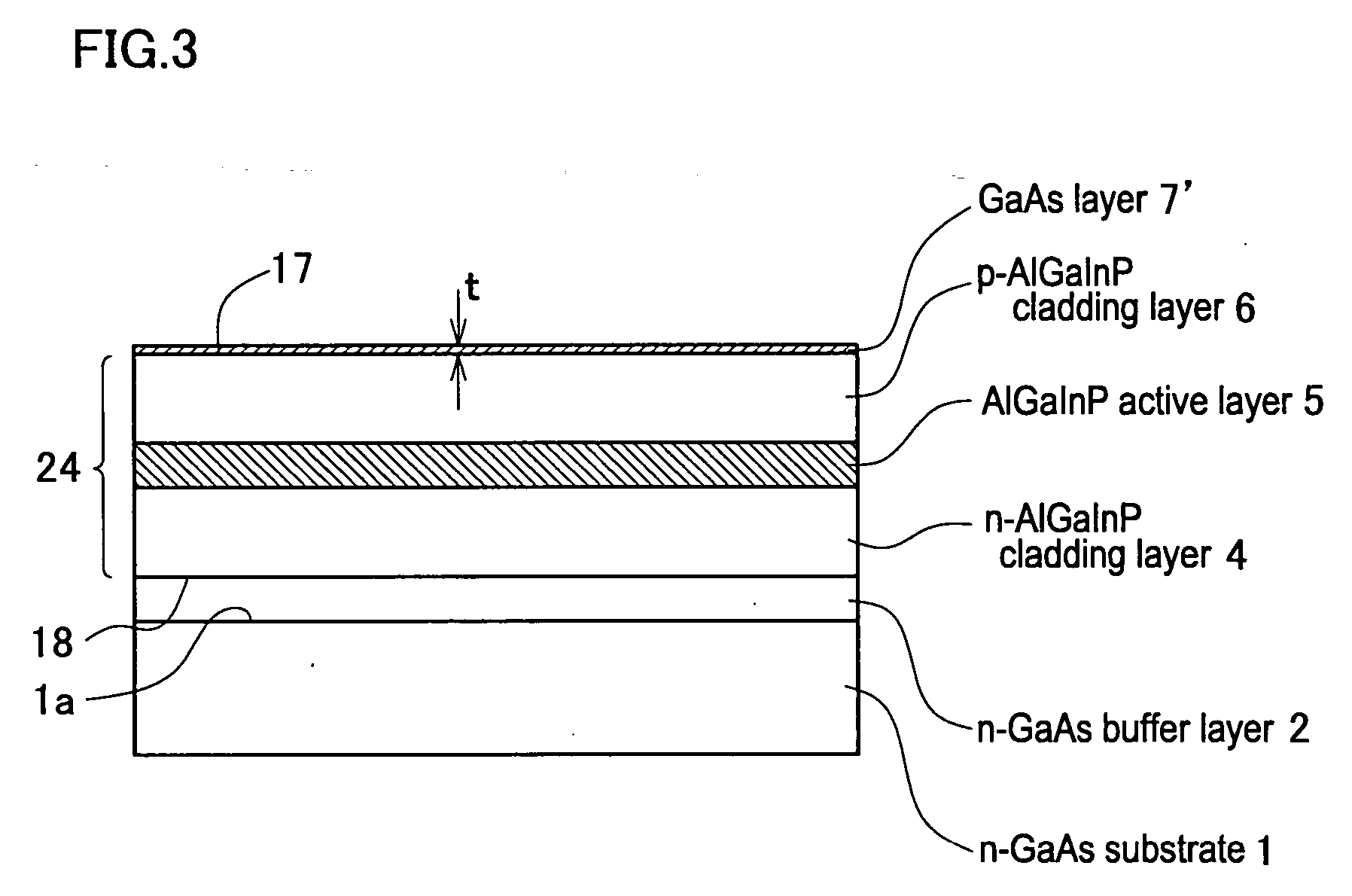
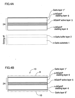
Method of fabricating light-emitting device and light-emitting device
PatentInactiveUS20050285127A1
Innovation
- A method involving the formation of a GaAs layer on the light-emitting layer section, followed by the deposition of an ITO transparent electrode layer and annealing to allow In diffusion, creating an In-containing GaAs contact layer with a graded In concentration, which reduces contact resistance and lattice mismatching, and enables efficient light emission and current spreading.
Supply Chain Considerations for ITO Alternatives
The global supply chain for ITO (Indium Tin Oxide) alternatives represents a critical consideration in the development and adoption of ITO-free electrode technologies. As indium remains a scarce and geopolitically sensitive material, manufacturers are increasingly seeking diversified material sources to mitigate supply risks and price volatility.
Alternative materials such as silver nanowires, carbon nanotubes, graphene, and metal mesh technologies present varying degrees of supply chain complexity. Silver nanowire production, while scaling rapidly, remains concentrated among a few key manufacturers in Asia and North America, potentially creating bottlenecks during high demand periods. The raw material sourcing for these alternatives generally offers greater geographical diversity compared to indium, which is predominantly mined in China.
Manufacturing processes for ITO alternatives often require specialized equipment and expertise, creating potential barriers to rapid adoption. However, many alternatives utilize more abundant materials with established supply networks, potentially offering long-term cost advantages. PEDOT:PSS, for instance, relies on organic compounds that can be synthesized through well-established chemical processes, reducing dependency on mining operations.
Regional manufacturing capabilities for ITO alternatives vary significantly. While East Asia maintains dominance in traditional display manufacturing infrastructure, emerging technologies present opportunities for manufacturing diversification. European and North American facilities have demonstrated increasing capabilities in specialized conductive materials production, particularly for next-generation flexible and printed electronics.
Regulatory considerations also impact supply chain decisions. Environmental regulations regarding chemical processing and waste management differ across regions, potentially affecting production costs and material availability. Additionally, sustainability certifications are increasingly influencing procurement decisions, with materials demonstrating lower environmental impact gaining preference among environmentally conscious manufacturers.
The transition to ITO-free electrodes necessitates careful consideration of supplier qualification processes. New materials often require extensive validation periods before full-scale implementation, creating temporary supply constraints during industry transition phases. Forward-thinking manufacturers are establishing dual-sourcing strategies and strategic partnerships with material developers to ensure continuity during technology transitions.
Cost structures for alternative materials differ substantially from traditional ITO. While initial material costs may be higher for some alternatives, simplified processing requirements and reduced energy consumption during manufacturing can offset these expenses, particularly at scale. The total cost of ownership analysis increasingly favors materials with stable pricing and reliable supply chains, even when unit costs exceed traditional solutions.
Sustainability Impact of ITO-Free Technologies
The transition to ITO-free electrode technologies represents a significant advancement in sustainable manufacturing practices within the electronics industry. Traditional indium tin oxide (ITO) production processes involve energy-intensive sputtering techniques and rely on indium, a scarce element with limited global reserves primarily concentrated in China. By eliminating ITO dependency, manufacturers can substantially reduce their environmental footprint across multiple dimensions.
Carbon emissions associated with ITO-free technologies show promising reductions, with recent life cycle assessments indicating up to 35% lower greenhouse gas emissions compared to conventional ITO manufacturing. This improvement stems primarily from lower processing temperatures and reduced energy requirements during electrode fabrication. Additionally, the elimination of rare earth mining operations necessary for indium extraction prevents associated environmental degradation, including soil erosion, water contamination, and habitat destruction.
Water conservation represents another critical sustainability advantage of ITO-free alternatives. Silver nanowire and PEDOT:PSS-based electrodes typically require 40-60% less water during production compared to traditional ITO manufacturing processes. This reduction is particularly significant in regions facing water scarcity challenges, where electronics manufacturing facilities often compete with agricultural and residential water needs.
The end-of-life management of electronic devices also benefits substantially from ITO-free technologies. Many alternative materials demonstrate enhanced recyclability profiles, with carbon-based electrodes showing particular promise for circular economy integration. Unlike ITO components, which often require specialized recycling processes to recover trace amounts of indium, graphene and carbon nanotube electrodes can be more readily incorporated into existing electronic waste recycling streams.
Supply chain resilience represents an often-overlooked sustainability dimension that ITO-free technologies directly address. By reducing dependency on geographically concentrated materials like indium, manufacturers can minimize transportation-related emissions while simultaneously reducing vulnerability to supply disruptions. This localization potential enables more regionally distributed manufacturing models that align with sustainable development goals.
Looking forward, the continued development of ITO-free electrode technologies promises to deliver additional sustainability benefits through materials innovation. Emerging bio-based conductive polymers derived from agricultural waste streams represent a particularly promising frontier, potentially transforming what is currently considered waste into valuable electronic components while simultaneously sequestering carbon throughout the product lifecycle.
Unlock deeper insights with Patsnap Eureka Quick Research — get a full tech report to explore trends and direct your research. Try now!
Generate Your Research Report Instantly with AI Agent
Supercharge your innovation with Patsnap Eureka AI Agent Platform!