Muriatic Acid's Role in the Production of Silicon Wafers
JUL 18, 20258 MIN READ
Generate Your Research Report Instantly with AI Agent
Patsnap Eureka helps you evaluate technical feasibility & market potential.
Silicon Wafer Etching Background and Objectives
Silicon wafer etching is a critical process in the semiconductor industry, with a rich history dating back to the mid-20th century. The evolution of this technology has been closely tied to the advancement of integrated circuits and the ever-increasing demand for smaller, more powerful electronic devices. Muriatic acid, also known as hydrochloric acid, has played a significant role in this process, particularly in the production of silicon wafers.
The primary objective of silicon wafer etching is to remove unwanted material from the surface of the wafer, creating precise patterns and structures necessary for the fabrication of semiconductor devices. This process is essential for achieving the desired electrical properties and performance characteristics of the final product. Over the years, the etching techniques have evolved from simple chemical etching to more sophisticated methods, including plasma etching and reactive ion etching.
Muriatic acid's involvement in silicon wafer production can be traced back to the early days of the semiconductor industry. Its ability to dissolve silicon dioxide and other impurities made it a valuable tool in the wafer cleaning and etching processes. As the industry progressed, the use of muriatic acid in combination with other chemicals, such as hydrogen peroxide and ammonium hydroxide, led to the development of more effective cleaning and etching solutions.
The technological trajectory of silicon wafer etching has been driven by the need for increased precision, uniformity, and efficiency in the manufacturing process. This has led to the development of advanced etching techniques that offer greater control over the etch rate, selectivity, and anisotropy. These advancements have enabled the production of increasingly complex and miniaturized semiconductor devices, supporting the continued growth of the electronics industry.
Current research and development efforts in silicon wafer etching are focused on addressing several key challenges. These include improving etch uniformity across larger wafer sizes, reducing defect rates, and developing more environmentally friendly etching processes. Additionally, there is a growing emphasis on developing etching techniques that are compatible with new materials and device architectures, such as those used in advanced logic and memory technologies.
As we look to the future, the objectives for silicon wafer etching technology continue to evolve. There is a strong push towards developing more precise and controllable etching processes that can support the fabrication of next-generation semiconductor devices. This includes the ability to create increasingly fine features, improve etch selectivity, and reduce damage to underlying layers. Furthermore, there is a growing interest in developing etching techniques that are more sustainable and have a lower environmental impact, aligning with broader industry goals for greener manufacturing processes.
Market Analysis for High-Purity Silicon Wafers
The high-purity silicon wafer market has experienced significant growth in recent years, driven by the increasing demand for advanced semiconductor devices across various industries. The global market for high-purity silicon wafers is expected to continue its upward trajectory, with a compound annual growth rate (CAGR) projected to remain strong through the next decade.
The primary drivers of this market growth include the rapid expansion of the electronics industry, particularly in emerging economies, and the growing adoption of advanced technologies such as 5G, artificial intelligence, and the Internet of Things (IoT). These technologies require increasingly sophisticated semiconductor components, which in turn rely on high-quality silicon wafers as their foundation.
The automotive sector has emerged as a key market for high-purity silicon wafers, with the rise of electric vehicles and autonomous driving systems creating new demand for advanced semiconductor devices. Additionally, the renewable energy sector, particularly solar panel manufacturing, continues to be a significant consumer of high-purity silicon wafers.
Geographically, Asia-Pacific dominates the high-purity silicon wafer market, with countries like China, Japan, South Korea, and Taiwan leading in both production and consumption. North America and Europe also represent substantial markets, driven by their advanced technology sectors and ongoing research and development activities.
The market is characterized by intense competition among a few major players, including Shin-Etsu Chemical, SUMCO Corporation, Siltronic AG, and GlobalWafers. These companies are continuously investing in research and development to improve wafer quality and production efficiency, as well as expanding their production capacities to meet growing demand.
One of the key trends in the high-purity silicon wafer market is the increasing demand for larger wafer diameters, with 300mm wafers becoming the industry standard and 450mm wafers on the horizon. This shift towards larger wafers is driven by the need for improved efficiency and cost-effectiveness in semiconductor manufacturing.
The role of muriatic acid (hydrochloric acid) in the production of silicon wafers is crucial, as it is used in various stages of the manufacturing process, including cleaning and etching. The demand for high-purity muriatic acid is therefore closely tied to the growth of the silicon wafer market, with manufacturers seeking ever-higher levels of purity to meet the exacting standards of advanced semiconductor production.
Current Challenges in Muriatic Acid Etching
Muriatic acid etching, a critical process in silicon wafer production, faces several significant challenges that impact the efficiency and quality of semiconductor manufacturing. One of the primary issues is the precise control of the etching rate and uniformity across the wafer surface. As wafer sizes increase and feature sizes decrease, maintaining consistent etching across large areas becomes increasingly difficult.
The formation of hydrogen bubbles during the etching process presents another major challenge. These bubbles can adhere to the wafer surface, causing localized areas of under-etching and resulting in non-uniform surface topography. This issue is particularly problematic for advanced node technologies where even minor surface irregularities can lead to device failures.
Environmental and safety concerns associated with the use of muriatic acid (hydrochloric acid) in large-scale manufacturing processes pose significant challenges. The corrosive nature of the acid requires stringent safety protocols and specialized handling equipment, increasing operational costs and complexity. Additionally, the disposal of spent acid solutions and the management of acidic fumes necessitate advanced waste treatment systems and air scrubbers to comply with environmental regulations.
The purity of muriatic acid used in semiconductor manufacturing is another critical factor. Trace contaminants in the acid can lead to surface defects or unwanted doping of the silicon substrate. Ensuring consistently high-purity acid supplies at industrial scales remains a persistent challenge for manufacturers.
Temperature control during the etching process is crucial for achieving reproducible results. Fluctuations in temperature can significantly affect the etching rate and selectivity. Maintaining precise temperature control across large wafer surfaces, especially in batch processing systems, presents ongoing engineering challenges.
The anisotropic nature of muriatic acid etching on silicon can lead to crystallographic-dependent etch rates. This property, while useful in some applications, can cause difficulties in achieving perfectly planar surfaces or creating specific three-dimensional structures required for advanced device architectures.
Lastly, the integration of muriatic acid etching with other process steps in the semiconductor manufacturing flow presents challenges in terms of process compatibility and contamination control. Residual acid or reaction products can interfere with subsequent processing steps, necessitating thorough cleaning procedures that add complexity and time to the overall manufacturing process.
Muriatic Acid Etching Process and Parameters
01 Industrial applications of muriatic acid
Muriatic acid, also known as hydrochloric acid, has various industrial applications. It is used in metal cleaning and pickling processes, particularly in the steel industry. The acid is also employed in the production of chemicals, water treatment, and as a pH regulator in various industrial processes.- Industrial applications of muriatic acid: Muriatic acid, also known as hydrochloric acid, has various industrial applications. It is used in metal cleaning and pickling processes, particularly in the steel industry. The acid is also employed in the production of chemicals, water treatment, and as a pH regulator in various industrial processes.
- Cleaning and etching applications: Muriatic acid is widely used in cleaning and etching applications. It is effective in removing rust, scale, and other deposits from metal surfaces. In the construction industry, it is used for cleaning masonry and concrete surfaces. The acid is also utilized in pool maintenance to adjust pH levels and remove stains.
- Production and handling of muriatic acid: The production of muriatic acid involves various processes, including the reaction of hydrogen and chlorine gases. Specialized equipment and safety measures are required for its production, storage, and handling due to its corrosive nature. Innovations in production methods focus on improving efficiency and reducing environmental impact.
- Environmental and safety considerations: Due to its corrosive nature, the use of muriatic acid requires careful handling and safety precautions. Environmental concerns related to its production and disposal have led to the development of more eco-friendly alternatives and improved waste management techniques. Proper neutralization and disposal methods are essential to minimize environmental impact.
- Innovations in muriatic acid formulations: Recent innovations in muriatic acid formulations focus on improving its effectiveness and safety for specific applications. These include the development of inhibited muriatic acid to reduce metal corrosion, gel formulations for better surface adhesion, and specialized blends for specific industrial processes. Research also aims to find more environmentally friendly alternatives with similar properties.
02 Cleaning and etching applications
Muriatic acid is widely used in cleaning and etching applications. It is effective in removing rust, scale, and other deposits from metal surfaces. In the construction industry, it is used for cleaning masonry and concrete surfaces. The acid is also utilized in pool maintenance to adjust pH levels and clean pool surfaces.Expand Specific Solutions03 Production and handling of muriatic acid
The production and handling of muriatic acid involve specific processes and safety measures. This includes methods for manufacturing high-purity hydrochloric acid, storage and transportation techniques, and safety protocols for handling this corrosive substance. Specialized equipment and materials are used to ensure safe production and handling.Expand Specific Solutions04 Environmental and waste management
Muriatic acid plays a role in environmental and waste management processes. It is used in the treatment of industrial wastewater, neutralization of alkaline waste, and in some air pollution control systems. Proper disposal and recycling methods for muriatic acid are essential to minimize environmental impact.Expand Specific Solutions05 Innovations in muriatic acid formulations
Recent innovations have led to the development of improved muriatic acid formulations. These include inhibited muriatic acid products that reduce metal corrosion, eco-friendly alternatives with reduced fumes and odors, and specialized blends for specific industrial applications. These innovations aim to enhance safety and efficiency in various uses of muriatic acid.Expand Specific Solutions
Key Players in Silicon Wafer Manufacturing
The market for muriatic acid in silicon wafer production is in a mature stage, with established players dominating the landscape. The global silicon wafer market size is projected to reach $14.98 billion by 2025, driven by increasing demand in semiconductor and electronics industries. Major companies like Shin-Etsu Handotai, SUMCO Corp, and Siltronic AG have advanced technological capabilities and significant market share. These firms, along with GlobalWafers and BASF, are continuously investing in R&D to improve wafer quality and production efficiency. The technology is well-established, but ongoing innovations focus on enhancing purity levels and reducing environmental impact, indicating a competitive and evolving market despite its maturity.
Shin-Etsu Handotai Co., Ltd.
Technical Solution: Shin-Etsu Handotai employs a sophisticated muriatic acid-based etching process in silicon wafer production. Their method involves precise control of acid concentration and temperature to achieve optimal surface smoothness. The company utilizes a multi-step etching technique, where muriatic acid is applied in varying concentrations to remove surface impurities and create a uniform crystal structure[1]. They have developed a proprietary recycling system that recovers and purifies used muriatic acid, reducing environmental impact and production costs[3]. Additionally, Shin-Etsu has implemented advanced automation in their acid handling systems, enhancing safety and consistency in the etching process[5].
Strengths: High-precision etching control, efficient acid recycling, and advanced automation. Weaknesses: Potentially higher initial equipment costs and the need for specialized handling of hazardous materials.
SUMCO Corp.
Technical Solution: SUMCO Corp. has developed an innovative muriatic acid-based cleaning and etching system for silicon wafer production. Their approach involves a two-stage process: an initial high-concentration acid bath for bulk material removal, followed by a low-concentration fine etching step for surface finishing[2]. SUMCO has also integrated real-time monitoring of acid concentration and impurity levels, allowing for dynamic adjustments during the etching process[4]. The company has patented a unique acid distribution system that ensures uniform application across large-diameter wafers, crucial for producing 300mm and 450mm wafers[6]. Furthermore, SUMCO has implemented a closed-loop acid management system that minimizes waste and reduces the environmental footprint of their manufacturing process[8].
Strengths: Advanced process control, capability for large-diameter wafers, and environmentally conscious acid management. Weaknesses: Complex system requiring highly skilled operators and potential for increased production time due to multi-stage processes.
Innovations in Muriatic Acid Etching Technology
Silicon wafer manufacturing method
PatentActiveTW201521105A
Innovation
- Introducing a hydrochloric acid cleaning step after the hydrofluoric acid cleaning to reduce fluoride ion residues on the silicon wafer surface.
- Implementing a two-step cleaning process (HF followed by HCl) to improve the overall cleanliness of the silicon wafer.
- Utilizing the properties of hydrochloric acid to effectively remove fluoride ions left by the hydrofluoric acid treatment.
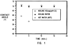
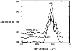
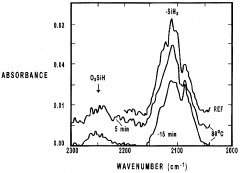
Methods for high temperature water rinsing and drying of silicon wafers after being cleaned in hydrofluoric acid
PatentInactiveUS5681397A
Innovation
- Treating silicon wafers with boiling water spiked with hydrochloric acid to create an aqueous hydrochloric acid solution with a pH of about 2.5, which minimizes reoxidation and surface roughening by controlling the OH- concentration and removing dissolved oxygen through gaseous bubbling.
Environmental Impact of Muriatic Acid Usage
The use of muriatic acid (hydrochloric acid) in silicon wafer production raises significant environmental concerns. The manufacturing process generates large volumes of acidic waste, which can have severe impacts on ecosystems if not properly managed. When released into water bodies, these acidic effluents can dramatically alter pH levels, leading to the destruction of aquatic habitats and the death of marine life.
Air pollution is another critical issue associated with muriatic acid usage. The production and handling of this chemical can release harmful vapors and aerosols into the atmosphere. These emissions contribute to air quality degradation, potentially causing respiratory problems in nearby communities and contributing to the formation of acid rain.
The disposal of spent muriatic acid and contaminated wastewater presents a substantial challenge. Improper disposal methods can lead to soil contamination, groundwater pollution, and long-term environmental damage. The acid's corrosive nature can also accelerate the deterioration of waste management infrastructure, potentially leading to leaks and further environmental contamination.
Energy consumption in the production and purification of muriatic acid for semiconductor-grade applications is another environmental concern. The high energy requirements contribute to increased carbon emissions, exacerbating climate change issues. Additionally, the transportation of large quantities of this hazardous material poses risks of accidental spills and releases during transit.
To mitigate these environmental impacts, the semiconductor industry has been implementing various strategies. These include developing closed-loop recycling systems for acid recovery and reuse, investing in advanced wastewater treatment technologies, and exploring alternative etching processes that reduce or eliminate the need for muriatic acid.
Regulatory bodies worldwide have imposed strict guidelines on the handling, storage, and disposal of muriatic acid in industrial processes. Companies are required to implement robust environmental management systems, conduct regular environmental impact assessments, and adhere to stringent emission standards. These measures aim to minimize the ecological footprint of silicon wafer production and protect surrounding ecosystems.
Research into green chemistry alternatives is gaining momentum, with scientists exploring bio-based etchants and environmentally friendly cleaning agents. These innovations could potentially reduce the reliance on harsh chemicals like muriatic acid, leading to more sustainable manufacturing processes in the semiconductor industry.
Safety Protocols in Acid-Based Wafer Production
Safety protocols in acid-based wafer production are critical to protect workers, equipment, and the environment from the hazards associated with handling corrosive substances like muriatic acid. These protocols encompass a range of measures designed to minimize risks and ensure safe operations throughout the silicon wafer production process.
Personal protective equipment (PPE) forms the first line of defense for workers. This includes chemical-resistant suits, gloves, boots, and face shields or goggles. Respiratory protection may also be necessary, depending on the concentration of acid vapors present. Regular training on proper PPE use and maintenance is essential to ensure its effectiveness.
Proper ventilation systems are crucial in acid-based wafer production facilities. These systems should be designed to effectively remove acid vapors and maintain air quality within safe limits. Regular monitoring of air quality and ventilation system performance is necessary to detect any potential issues promptly.
Acid storage and handling procedures must be strictly followed. This includes using appropriate containers made of acid-resistant materials, implementing proper labeling and segregation practices, and establishing designated storage areas with secondary containment measures. Transfer of acids should be performed using closed systems or specialized equipment to minimize the risk of spills or splashes.
Emergency response plans and equipment are vital components of safety protocols. This includes easily accessible eyewash stations, safety showers, and spill containment kits. Workers must be trained in emergency procedures and the use of this equipment. Regular drills should be conducted to ensure readiness in case of an incident.
Waste management and disposal procedures for acid-containing materials must comply with environmental regulations. This may involve neutralization processes, specialized waste treatment facilities, or contracted disposal services. Proper documentation and tracking of waste streams are essential for regulatory compliance and environmental protection.
Regular safety audits and inspections should be conducted to identify potential hazards, assess the effectiveness of existing safety measures, and implement improvements as needed. This proactive approach helps maintain a culture of safety and continuous improvement in acid-based wafer production facilities.
Unlock deeper insights with Patsnap Eureka Quick Research — get a full tech report to explore trends and direct your research. Try now!
Generate Your Research Report Instantly with AI Agent
Supercharge your innovation with Patsnap Eureka AI Agent Platform!