Optimizing RRAM for Machine Learning: Speed and Capacity
SEP 10, 20259 MIN READ
Generate Your Research Report Instantly with AI Agent
Patsnap Eureka helps you evaluate technical feasibility & market potential.
RRAM Technology Evolution and Optimization Goals
Resistive Random Access Memory (RRAM) technology has evolved significantly since its conceptualization in the early 2000s. Initially developed as a non-volatile memory alternative to traditional flash memory, RRAM has progressed through several technological generations, each addressing specific limitations of previous iterations. The first generation focused primarily on proof-of-concept demonstrations with simple metal-oxide structures, while subsequent generations have increasingly refined material compositions, switching mechanisms, and fabrication processes.
The evolution trajectory of RRAM technology has been characterized by continuous improvements in endurance, retention time, and power consumption. Early RRAM devices suffered from reliability issues, including limited write/erase cycles and data retention problems. However, advancements in material science and device engineering have led to substantial improvements, with modern RRAM devices capable of achieving endurance cycles exceeding 10^12 and retention times of over 10 years at elevated temperatures.
A critical milestone in RRAM development was the transition from binary to multi-level cell capabilities, enabling higher storage densities. This advancement has been particularly significant for machine learning applications, where high-density storage is essential for implementing neural network weights efficiently. The ability to store multiple bits per cell has positioned RRAM as a promising technology for in-memory computing architectures.
Current optimization goals for RRAM in machine learning contexts focus on two primary dimensions: speed and capacity. Speed optimization aims to reduce read/write latencies to nanosecond ranges, enabling real-time inference and training operations. This involves refining the switching dynamics of the resistive elements and developing more efficient peripheral circuitry for addressing and sensing operations.
Capacity optimization efforts target increasing storage density while maintaining reliability. This includes developing more sophisticated multi-level cell technologies, improving uniformity across large arrays, and implementing 3D integration techniques to increase effective storage capacity per unit area. The goal is to achieve storage densities comparable to or exceeding those of NAND flash while maintaining the speed advantages inherent to RRAM technology.
Another crucial optimization direction involves reducing the energy consumption per operation, which is particularly important for edge computing applications where power constraints are significant. Research efforts are focused on lowering the operating voltages and currents required for reliable switching while maintaining sufficient margins between resistance states.
The convergence of these optimization goals aims to position RRAM as the ideal memory technology for next-generation machine learning hardware, enabling efficient implementation of both training and inference operations. The ultimate vision is to create memory systems that can perform computational tasks directly within the memory array, eliminating the traditional von Neumann bottleneck that separates computation from storage.
Market Demand Analysis for ML-Optimized Memory
The machine learning (ML) market is experiencing unprecedented growth, driving demand for specialized memory solutions that can handle the intensive computational requirements of AI algorithms. The global AI chip market, which includes memory components optimized for ML, reached $15 billion in 2023 and is projected to grow at a CAGR of 40% through 2028, highlighting the expanding need for ML-optimized memory technologies like RRAM.
Edge computing represents a particularly promising segment for RRAM adoption in ML applications. With over 30 billion IoT devices expected to be deployed by 2025, there is growing demand for memory solutions that can enable on-device ML inference with minimal power consumption. Market research indicates that 65% of enterprise AI deployments will incorporate edge processing by 2025, creating substantial opportunities for RRAM technologies optimized for machine learning workloads.
Data centers represent another significant market for ML-optimized memory solutions. The hyperscale data center market is growing at 27% annually, with AI workloads consuming an increasing share of computational resources. Memory bandwidth and capacity limitations have emerged as critical bottlenecks in ML training and inference, with 78% of data center operators identifying memory constraints as a primary challenge for AI deployment.
The automotive sector presents a rapidly expanding market for ML-optimized memory, particularly for autonomous driving systems. Level 3+ autonomous vehicles require approximately 8TB of data processing per day, creating demand for high-speed, high-capacity memory solutions that can operate reliably in automotive environments. Industry forecasts suggest the automotive AI hardware market will reach $12 billion by 2027, with memory components representing a significant portion.
Healthcare applications of machine learning are driving demand for specialized memory solutions that can handle complex neural networks while maintaining patient data privacy. The healthcare AI market is expected to reach $45 billion by 2026, with applications ranging from medical imaging analysis to drug discovery requiring memory architectures that can efficiently process large datasets.
Mobile and consumer electronics manufacturers are increasingly integrating on-device ML capabilities, creating demand for memory solutions that balance performance with power efficiency. The market for ML-capable mobile processors grew by 45% in 2023, with memory bandwidth identified as a key constraint for more advanced on-device AI applications. RRAM's potential for high-density, low-power operation makes it particularly attractive for this segment.
RRAM Technical Challenges for ML Applications
RRAM (Resistive Random Access Memory) technology faces several critical challenges when applied to machine learning applications, particularly in terms of optimizing speed and capacity. The non-linear and stochastic switching behavior of RRAM cells presents a fundamental obstacle, causing inconsistent performance during read and write operations that can significantly impact the accuracy of neural network computations.
Variability issues manifest in several forms, including cycle-to-cycle variations where the same cell exhibits different resistance values across programming cycles, and device-to-device variations where nominally identical cells show different electrical characteristics. These inconsistencies create substantial challenges for implementing precise weight storage in neural network applications, where even small deviations can propagate and magnify errors throughout the network.
The endurance limitations of current RRAM technologies present another significant hurdle. Most commercial RRAM cells can withstand approximately 10^6 to 10^9 write cycles before experiencing performance degradation, which falls short of the requirements for intensive machine learning training workloads that may demand billions of weight updates. This limitation restricts RRAM's applicability in online learning scenarios where weights require frequent modifications.
Energy efficiency, while generally superior to traditional memory technologies, remains suboptimal for large-scale machine learning deployments. The write operations in particular consume significant power, creating thermal management challenges in densely packed arrays. This becomes especially problematic when implementing large neural networks that require extensive memory resources.
The speed-capacity tradeoff represents perhaps the most fundamental challenge. While RRAM offers higher density than SRAM, it operates at slower speeds, creating a bottleneck for high-throughput machine learning applications. Conversely, optimizing for speed often requires architectural compromises that reduce overall storage capacity, limiting the size and complexity of implementable neural networks.
Integration challenges with conventional CMOS technology further complicate RRAM adoption. The fabrication processes, operating voltages, and signal conditioning requirements for RRAM often differ significantly from standard CMOS processes, necessitating complex interface circuitry that increases chip area and power consumption while potentially introducing additional performance bottlenecks.
Addressing these technical challenges requires multidisciplinary approaches spanning materials science, device physics, circuit design, and machine learning algorithm development. Recent research has focused on novel materials and cell structures to improve uniformity and endurance, as well as specialized programming schemes that can compensate for device non-idealities.
Current RRAM Solutions for Machine Learning
01 RRAM Speed Characteristics and Optimization
RRAM devices offer high-speed operation capabilities with fast switching times between resistance states. The speed performance can be optimized through various techniques including material selection, device structure design, and pulse engineering. These optimizations enable RRAM to achieve read/write speeds comparable to or better than conventional memory technologies, making it suitable for high-performance computing applications. The switching speed is primarily determined by the ion migration process within the resistive switching layer.- RRAM Speed Characteristics and Optimization: RRAM devices offer high-speed operation capabilities with fast switching times between resistance states. The speed performance can be optimized through various approaches including material selection, device structure design, and pulse engineering. These optimizations enable RRAM to achieve read/write speeds comparable to or better than conventional memory technologies, making it suitable for high-performance computing applications. The switching speed is primarily determined by the ion migration process, which can be controlled by adjusting the applied voltage and pulse duration.
- RRAM Storage Capacity Enhancement: Various techniques have been developed to increase the storage capacity of RRAM devices. These include multi-level cell (MLC) approaches that allow storing multiple bits per cell by utilizing different resistance states, 3D stacking architectures that increase density without expanding the footprint, and crossbar array structures that maximize cell density. Advanced fabrication techniques and material innovations enable higher integration density, contributing to increased storage capacity while maintaining reliability and performance characteristics.
- Material Innovations for RRAM Performance: Novel materials and material combinations significantly impact both the speed and capacity of RRAM devices. Metal oxides, such as HfOx, TaOx, and TiOx, demonstrate superior switching characteristics. Two-dimensional materials and nanocomposites offer enhanced performance through improved ion mobility and controlled defect engineering. Material interface engineering plays a crucial role in optimizing the formation and rupture of conductive filaments, directly affecting switching speed and reliability. These material innovations contribute to faster switching speeds and higher storage densities.
- RRAM Architecture and Integration Solutions: Advanced RRAM architectures have been developed to maximize both speed and capacity. These include crossbar arrays that minimize cell area and parasitic effects, 3D vertical stacking that increases density without expanding footprint, and hybrid memory systems that combine RRAM with conventional memory technologies. Integration solutions address challenges related to sneak path currents, selector devices, and peripheral circuitry optimization. These architectural innovations enable RRAM to achieve higher capacity while maintaining or improving operational speed.
- Reliability and Endurance Improvements: Enhancing reliability and endurance is critical for practical RRAM applications requiring both high speed and capacity. Various approaches have been developed including optimized programming schemes that reduce stress on the memory cells, error correction techniques that improve data retention, and feedback mechanisms that maintain consistent performance over time. Pulse engineering methods control the filament formation process, resulting in more stable resistance states. These improvements ensure that RRAM devices maintain their speed and capacity advantages over extended operational lifetimes.
02 RRAM Storage Capacity Enhancement
Various approaches have been developed to increase the storage capacity of RRAM devices. These include multi-level cell (MLC) architectures that store multiple bits per cell by utilizing different resistance states, 3D stacking technologies that increase density through vertical integration, and crossbar array structures that maximize the number of memory cells per unit area. These techniques collectively enable RRAM to achieve high storage densities suitable for next-generation memory applications.Expand Specific Solutions03 Material Innovations for RRAM Performance
Advanced materials play a crucial role in determining RRAM speed and capacity. Various oxide materials, metal oxides, and novel two-dimensional materials have been investigated to enhance switching characteristics. The selection of electrode materials and switching layer composition significantly impacts the resistance switching behavior, retention time, and endurance. Engineered material interfaces and doping strategies can further optimize the performance parameters of RRAM devices.Expand Specific Solutions04 RRAM Architecture and Integration
Novel RRAM architectures have been developed to maximize both speed and capacity. These include crossbar arrays, selector-based architectures to minimize sneak path currents, and hybrid memory systems that combine RRAM with other memory technologies. Integration techniques with CMOS technology enable high-density memory arrays while addressing challenges related to parasitic effects and signal integrity. Advanced 3D integration approaches further enhance the overall memory density.Expand Specific Solutions05 RRAM Control and Operation Methods
Specialized control methods and operation schemes have been developed to optimize RRAM speed and capacity. These include advanced programming algorithms that enhance switching speed while maintaining reliability, read schemes that accelerate data retrieval, and error correction techniques that improve data integrity. Pulse engineering approaches optimize the voltage amplitude, duration, and shape to achieve faster switching times while reducing power consumption. These methods collectively enhance the overall performance of RRAM devices.Expand Specific Solutions
Key Industry Players in RRAM Technology
The RRAM (Resistive Random Access Memory) market for machine learning applications is in a growth phase, with increasing demand for faster, higher-capacity memory solutions. The global market is expanding rapidly as AI workloads require more efficient memory architectures. Leading semiconductor companies like Huawei, Intel, Samsung, and Micron are investing heavily in RRAM technology optimization, while specialized players such as Everspin Technologies and CrossBar are developing innovative solutions specifically targeting ML applications. Research institutions including IMEC, Fudan University, and USC collaborate with industry partners to overcome technical challenges in speed, endurance, and capacity. The technology is approaching commercial maturity, with companies like TSMC and Qualcomm integrating RRAM into their product roadmaps to address the growing computational demands of machine learning applications.
Micron Technology, Inc.
Technical Solution: Micron has developed advanced 3D RRAM technology optimized for machine learning workloads. Their approach utilizes a cross-point architecture that enables high-density storage with multiple layers stacked vertically. Micron's RRAM technology features sub-5ns read latency and approximately 20ns write latency, providing significant performance advantages for ML inference operations. The company has implemented innovative materials engineering, using proprietary metal oxide compositions that enhance switching reliability and reduce variability between cells. Micron's RRAM solution incorporates on-chip processing capabilities that enable in-memory computing for matrix multiplication operations, a critical function in neural network processing. This reduces data movement between memory and processing units, significantly improving energy efficiency. Their technology demonstrates 10^6 endurance cycles while maintaining a 10-year data retention capability at operating temperatures.
Strengths: Vertical stacking capability enables high storage density; extremely low read latency benefits ML inference; in-memory computing capabilities reduce system power consumption. Weaknesses: Write endurance still lower than competing memory technologies; resistance drift over time requires compensation algorithms.
Samsung Electronics Co., Ltd.
Technical Solution: Samsung has developed a comprehensive RRAM solution for machine learning applications focusing on both speed and capacity optimization. Their technology employs a unique filament formation mechanism that enables faster switching speeds while maintaining data integrity. Samsung's RRAM architecture incorporates a hierarchical memory design with multiple tiers of RRAM cells optimized for different aspects of ML workloads - high-speed cells for frequently accessed weights and high-density cells for model storage. The company has achieved read latencies below 10ns and write speeds of approximately 30ns in their high-performance RRAM tier. Samsung has also implemented advanced multi-level cell (MLC) technology in their RRAM, storing 2-3 bits per cell to maximize storage density. Their manufacturing process integrates RRAM layers directly above conventional CMOS logic, creating a true processing-in-memory solution that dramatically reduces the energy costs associated with data movement in ML applications.
Strengths: Hierarchical memory architecture optimized for different ML requirements; industry-leading MLC technology increases bit density; true processing-in-memory capabilities. Weaknesses: MLC implementation increases complexity of programming algorithms; reliability challenges at advanced technology nodes below 20nm.
Critical Patents and Research in RRAM Optimization
Resistive random access memory device
PatentActiveUS20230140134A1
Innovation
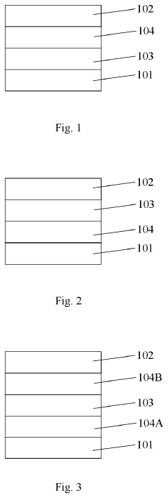
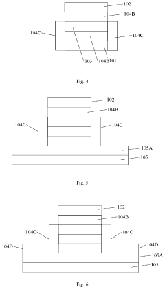
- The introduction of a tapered or needle-like shaped top electrode region with an oxygen-rich dielectric layer, which enhances filament formation predictability and maintains a high concentration of oxygen ions to compensate for losses during frequent switching operations.


Resistive random access memory and manufacturing method thereof
PatentActiveUS20210028358A1
Innovation
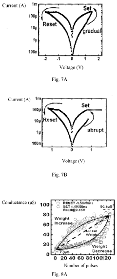
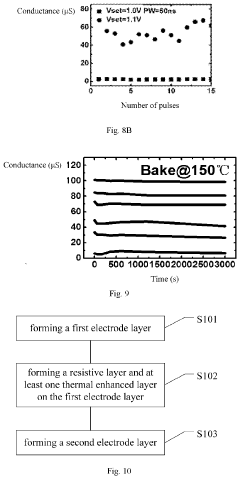
- Incorporating a thermal enhanced layer with lower thermal conductivity than the electrodes, positioned adjacent to the resistive layer, to slow down heat loss and promote the formation of dispersed conductive filaments, allowing continuous and bidirectional linear changes in conductance.
Energy Efficiency Considerations for RRAM-based ML
Energy efficiency has emerged as a critical factor in the widespread adoption of RRAM (Resistive Random Access Memory) for machine learning applications. As ML workloads continue to grow in complexity and scale, the energy consumption of computing systems has become a significant bottleneck, particularly for edge devices and data centers. RRAM offers inherent advantages in this domain due to its non-volatile nature, which eliminates static power consumption when not actively performing operations.
The energy profile of RRAM-based ML systems can be analyzed across three key dimensions: read operations, write operations, and standby power. Read operations in RRAM typically consume 10-100x less energy compared to conventional DRAM, with energy requirements as low as 0.1-1 pJ per bit access. Write operations, while more energy-intensive than reads, still demonstrate 5-50x improvement over flash memory alternatives, typically requiring 1-10 pJ per bit.
Architectural innovations have further enhanced RRAM's energy efficiency. In-memory computing paradigms, where computations are performed directly within RRAM arrays, substantially reduce the energy costs associated with data movement between memory and processing units. This approach eliminates the von Neumann bottleneck, which can account for up to 70% of energy consumption in conventional computing architectures.
Material engineering advances have also contributed significantly to improving RRAM's energy profile. Novel switching materials such as HfOx and TaOx have demonstrated switching energies below 0.1 pJ, while maintaining reliable operation. Multi-level cell configurations, which store multiple bits per cell, further improve energy efficiency by increasing storage density without proportional increases in power consumption.
Temperature sensitivity remains a challenge for RRAM energy efficiency. Operating temperatures significantly impact both performance and power consumption, with higher temperatures generally leading to increased leakage currents. Recent research has focused on developing temperature-compensated designs that maintain consistent energy profiles across a wide operating range of -40°C to 125°C.
Scaling considerations present another important dimension of RRAM energy efficiency. As device dimensions shrink below 10nm, quantum effects begin to dominate, potentially increasing variability and reducing energy efficiency. However, 3D integration approaches offer promising pathways to maintain or improve energy efficiency while increasing storage density through vertical stacking of memory elements.
Looking forward, hybrid approaches combining RRAM with other emerging technologies such as spintronics or photonics may unlock new frontiers in energy-efficient ML computing. These heterogeneous systems could leverage the complementary strengths of different technologies to optimize both performance and energy consumption for specific ML workloads.
Scalability and Integration Challenges
As RRAM technology advances toward machine learning applications, significant scalability and integration challenges must be addressed. The miniaturization of RRAM cells faces fundamental physical limitations, particularly when cell dimensions approach sub-10nm scales. At these dimensions, variability in switching behavior increases dramatically, compromising reliability and predictability essential for ML workloads. This variability stems from stochastic filament formation processes that become more pronounced at smaller scales, creating inconsistent resistance states across arrays.
Integration with CMOS technology presents another substantial hurdle. While RRAM offers potential for back-end-of-line integration, thermal budget constraints during fabrication can lead to material degradation and performance inconsistencies. The interface between RRAM cells and traditional CMOS circuitry introduces parasitic capacitances and resistances that degrade overall system performance, particularly affecting the speed requirements of ML applications.
3D integration approaches offer promising solutions to density limitations but introduce complex fabrication challenges. Vertical stacking of RRAM arrays requires precise alignment techniques and specialized etching processes that maintain consistent electrical characteristics throughout the structure. Heat dissipation becomes increasingly problematic in 3D configurations, potentially limiting operational speeds during intensive computational tasks common in machine learning inference.
Scaling RRAM for large-scale ML deployments also faces interconnect bottlenecks. As array sizes increase, the resistance of word and bit lines becomes a limiting factor for access speed. Advanced interconnect materials and novel architectural approaches, such as hierarchical bit-line structures, are being explored to mitigate these effects, but add complexity to the manufacturing process.
The non-uniformity of programming and read operations across large arrays presents additional challenges. Voltage drops along word and bit lines create position-dependent variations in programming conditions, resulting in non-uniform resistance distributions that complicate ML algorithm implementation. Compensation circuits can partially address these issues but consume additional chip area and power.
Yield management represents a critical economic challenge for RRAM scaling. Defect densities must be minimized to ensure economically viable production of large arrays. Current manufacturing processes still struggle with consistency across wafers, making high-volume production of ML-optimized RRAM challenging. Advanced defect detection and redundancy schemes are being developed to improve yield rates, though these add overhead to both design and fabrication processes.
Unlock deeper insights with Patsnap Eureka Quick Research — get a full tech report to explore trends and direct your research. Try now!
Generate Your Research Report Instantly with AI Agent
Supercharge your innovation with Patsnap Eureka AI Agent Platform!