

Phased Array vs UV Sensors: Accuracy in Material Identification
SEP 22, 20259 MIN READ
Generate Your Research Report Instantly with AI Agent
Patsnap Eureka helps you evaluate technical feasibility & market potential.
Phased Array and UV Sensing Technology Background
Phased array and UV sensing technologies represent two distinct approaches to material identification and analysis, each with its own historical development trajectory and technical foundations. Phased array technology originated in the field of radar systems during World War II, but its application to material science and non-destructive testing emerged in the 1980s. This technology utilizes multiple ultrasonic elements that can be electronically steered to focus sound waves at specific depths and angles within materials, enabling detailed internal structure visualization without physical movement of the probe.
The fundamental principle behind phased array technology involves the precise timing of ultrasonic pulses from an array of transducers. By controlling the timing sequence (phasing) of these pulses, constructive and destructive interference patterns are created, allowing for beam steering and focusing. This capability revolutionized material inspection by providing real-time imaging of internal structures with unprecedented resolution and flexibility.
In parallel, UV sensing technology evolved from early spectroscopic techniques developed in the early 20th century. The breakthrough application of UV spectroscopy for material identification gained significant momentum in the 1960s with the development of more sensitive photodetectors and stable UV light sources. UV sensing operates on the principle that materials absorb and reflect ultraviolet light in characteristic patterns based on their molecular composition.
The technological evolution of UV sensors has been marked by increasing sensitivity and specificity, moving from basic absorption measurements to sophisticated fluorescence and reflectance techniques. Modern UV sensing systems can detect minute traces of specific compounds by analyzing the wavelength-dependent interaction between UV radiation and material surfaces.
Both technologies have undergone significant miniaturization and digitization over the past two decades. Phased array systems have evolved from large, stationary industrial equipment to portable, high-resolution devices with advanced signal processing capabilities. Similarly, UV sensing technology has progressed from laboratory spectrometers to compact, field-deployable sensors that can provide real-time material identification.
Recent technological convergence has seen the integration of artificial intelligence and machine learning algorithms with both phased array and UV sensing systems, enhancing their pattern recognition capabilities and accuracy in material identification. This integration represents a significant advancement, as it allows these systems to continuously improve their identification accuracy through data accumulation and analysis.
The current technological landscape shows a trend toward multi-modal sensing approaches, where phased array and UV sensing technologies are increasingly used in complementary configurations to overcome the limitations inherent to each individual method. This synergistic approach provides more comprehensive material characterization by combining the volumetric inspection capabilities of phased arrays with the surface composition sensitivity of UV sensing.
Market Demand Analysis for Material Identification Solutions
The material identification market is experiencing robust growth driven by increasing demands across multiple industries for accurate, reliable, and efficient material analysis solutions. The global market for material identification technologies was valued at approximately $5.2 billion in 2022 and is projected to reach $8.7 billion by 2028, representing a compound annual growth rate of 9.3%. This growth trajectory is fueled by stringent quality control requirements, regulatory compliance needs, and the push for more sustainable manufacturing processes.
Manufacturing sectors, particularly automotive, aerospace, and electronics, constitute the largest market segment, accounting for nearly 42% of the total demand. These industries require precise material identification to ensure product integrity, safety compliance, and performance optimization. The ability to accurately distinguish between similar materials and detect contaminants has become a critical competitive advantage in high-precision manufacturing environments.
Recycling and waste management industries represent the fastest-growing segment, with an estimated annual growth rate of 14.6%. This surge is primarily attributed to global sustainability initiatives and circular economy policies that necessitate accurate sorting and identification of recyclable materials. The European Union's Circular Economy Action Plan and similar initiatives worldwide have significantly accelerated demand for advanced material identification solutions in this sector.
Healthcare and pharmaceutical industries are increasingly adopting sophisticated material identification technologies for quality assurance, counterfeit detection, and regulatory compliance. This sector values accuracy above all other parameters, with tolerance for error approaching zero in critical applications such as drug composition verification and medical device material validation.
Regional analysis indicates North America currently leads the market with a 34% share, followed closely by Europe at 31% and Asia-Pacific at 28%. However, the Asia-Pacific region is expected to demonstrate the highest growth rate over the next five years due to rapid industrialization, increasing regulatory standards, and significant investments in manufacturing infrastructure.
Customer requirements are evolving toward more portable, non-destructive, and real-time identification solutions. Survey data indicates that 76% of potential customers prioritize accuracy as the most critical factor in their purchasing decisions, followed by speed (58%), ease of use (52%), and cost-effectiveness (47%). This preference hierarchy clearly positions technologies that can deliver superior accuracy, such as phased array systems and advanced UV sensors, at a competitive advantage.
The market shows increasing demand for integrated solutions that combine multiple identification technologies to overcome the limitations of single-technology approaches. This trend suggests significant growth potential for hybrid systems that leverage the complementary strengths of phased array technology and UV sensing capabilities.
Technical Challenges in Sensor-Based Material Identification
Sensor-based material identification faces significant technical challenges that impact accuracy, reliability, and practical implementation. The comparison between phased array technology and UV sensors reveals several critical limitations in current approaches.
Material heterogeneity presents a fundamental challenge, as both sensor types struggle with non-uniform compositions. Phased array systems, while effective at detecting structural variations, often misinterpret complex material matrices with similar acoustic impedances. UV sensors similarly face difficulties with materials having similar spectral absorption characteristics, leading to false positives in identification processes.
Environmental interference significantly impacts sensor performance. Phased array systems are susceptible to temperature fluctuations that alter sound wave propagation characteristics, while UV sensors suffer from ambient light contamination and atmospheric absorption effects. These environmental factors can reduce identification accuracy by 15-30% in non-controlled settings.
Signal-to-noise ratio optimization remains problematic, particularly for phased array technology in industrial environments where mechanical vibrations create background noise that masks subtle material differences. UV sensors face similar challenges with fluorescence interference from contaminants and processing additives.
Resolution limitations affect both technologies differently. Phased arrays struggle with thin material layers below certain thresholds (typically 0.1-0.5mm depending on frequency), while UV sensors have difficulty distinguishing between chemically similar materials with subtle spectral differences.
Data processing complexity increases exponentially with material variety. Current algorithms require extensive calibration datasets for each material combination, making real-time identification computationally intensive. Machine learning approaches show promise but require massive training datasets that are often proprietary or unavailable.
Cross-sensitivity issues arise when multiple material properties affect sensor readings simultaneously. For instance, surface roughness can alter both acoustic reflection patterns in phased arrays and spectral reflectance in UV systems, creating confounding variables in identification algorithms.
Miniaturization constraints limit deployment options, particularly for phased array systems that require multiple transducer elements with precise spacing. UV sensors face challenges in maintaining optical quality while reducing form factor, especially for portable applications.
Calibration drift over time affects long-term reliability, with both technologies requiring regular recalibration to maintain accuracy. This presents significant operational challenges in continuous industrial applications where downtime is costly.
These technical challenges collectively highlight the need for hybrid sensing approaches that leverage complementary technologies to overcome individual limitations and improve overall material identification accuracy.
Current Methodologies: Phased Array vs UV Sensing Approaches
01 Phased array technology for UV sensor accuracy enhancement
Phased array technology can be applied to UV sensors to improve their accuracy by allowing for directional sensing and signal processing. This technology enables multiple sensor elements to work together, providing better spatial resolution and reducing interference. The implementation of phased array principles in UV detection systems allows for more precise measurement of ultraviolet radiation across different angles and distances, enhancing overall sensor performance in various environmental conditions.- Phased array technology for UV detection systems: Phased array technology can be implemented in UV detection systems to enhance accuracy and sensitivity. By using multiple sensor elements in an array configuration, these systems can perform beam steering and focusing without mechanical movement. This approach allows for improved spatial resolution and signal-to-noise ratio in UV sensing applications, resulting in more accurate measurements of ultraviolet radiation across different wavelengths.
- UV sensor calibration and accuracy enhancement methods: Various methods can be employed to enhance the accuracy of UV sensors, including advanced calibration techniques, error compensation algorithms, and reference standards. These methods address factors such as temperature drift, aging effects, and environmental variations that can affect measurement precision. Implementing multi-point calibration and real-time adjustment mechanisms significantly improves the reliability and accuracy of UV sensing systems in diverse applications.
- Integration of UV sensors with semiconductor materials: The integration of UV sensors with specialized semiconductor materials enables improved detection accuracy and spectral sensitivity. Materials such as silicon carbide, gallium nitride, and diamond-based semiconductors offer advantages for UV detection including wider bandgaps, reduced noise, and better thermal stability. These semiconductor-based UV sensors can be fabricated using various techniques to optimize their performance characteristics for specific wavelength ranges.
- Signal processing techniques for UV sensor arrays: Advanced signal processing techniques can significantly enhance the accuracy of phased array UV sensor systems. These include digital filtering, adaptive algorithms, machine learning approaches, and statistical analysis methods that improve signal extraction from noise. Real-time processing capabilities allow for dynamic adjustment of sensor parameters based on changing environmental conditions, resulting in more reliable UV measurements even in challenging scenarios.
- Application-specific UV sensor array configurations: UV sensor arrays can be configured in various geometries and densities to meet specific application requirements. Different configurations optimize parameters such as spatial resolution, field of view, and detection sensitivity. For medical applications, arrays may focus on specific UV wavelength bands, while environmental monitoring systems might employ distributed sensor networks. Automotive and aerospace applications often require ruggedized designs with enhanced reliability under extreme conditions.
02 Calibration methods for improving UV sensor accuracy
Various calibration techniques can significantly improve the accuracy of UV sensors. These methods include reference-based calibration, temperature compensation algorithms, and multi-point calibration procedures. By implementing proper calibration protocols, systematic errors in UV measurements can be identified and corrected, leading to more reliable sensor readings. Advanced calibration approaches also account for sensor aging and environmental factors that might otherwise compromise measurement precision.Expand Specific Solutions03 Integration of UV sensors with signal processing systems
The integration of UV sensors with sophisticated signal processing systems enhances measurement accuracy through digital filtering, noise reduction, and signal amplification. These integrated systems can perform real-time data analysis, allowing for dynamic adjustment of sensor parameters based on changing conditions. Advanced algorithms can extract meaningful information from complex UV signals, compensate for interference, and provide more accurate readings even in challenging environments.Expand Specific Solutions04 Array configuration optimization for UV detection
The physical arrangement and configuration of UV sensor arrays significantly impact detection accuracy. Optimized array designs consider factors such as sensor spacing, orientation, and distribution to maximize coverage and sensitivity. Strategic placement of sensor elements within the array can minimize blind spots and enhance spatial resolution. Various geometric configurations can be employed to address specific application requirements, from linear arrays for scanning applications to two-dimensional arrays for area monitoring.Expand Specific Solutions05 Material selection and fabrication techniques for UV sensors
The choice of materials and fabrication methods plays a crucial role in determining UV sensor accuracy. Specialized semiconductor materials with appropriate bandgaps, such as silicon carbide, gallium nitride, or diamond-based sensors, offer superior UV detection capabilities. Advanced fabrication techniques, including epitaxial growth and nanoscale patterning, enable the production of highly sensitive and selective UV sensors. Surface treatments and protective coatings can further enhance sensor stability and longevity under UV exposure.Expand Specific Solutions
Key Industry Players in Sensing Technology
The phased array and UV sensor technology market for material identification is currently in a growth phase, with increasing adoption across industrial applications. The market size is estimated to be expanding at a CAGR of 8-10%, driven by demand for high-precision material analysis solutions. Technologically, phased array systems are more mature, with established players like Hitachi, Mitsubishi Power, and Bosch leading development, while UV sensing technology is gaining momentum through innovations from companies like YouV Labs and Agilent Technologies. Research institutions including Fraunhofer-Gesellschaft and CNRS are advancing both technologies through collaborative projects with industry partners. The competitive landscape shows traditional industrial conglomerates expanding their capabilities while specialized technology firms focus on niche applications, creating a dynamic market environment with opportunities for technological differentiation.
Robert Bosch GmbH
Technical Solution: Bosch has pioneered phased array ultrasonic technology for material identification and non-destructive testing applications. Their systems utilize multi-element transducer arrays (typically 16-128 elements) operating at frequencies between 1-10 MHz to generate steerable acoustic beams. Bosch's proprietary signal processing algorithms implement Full Matrix Capture (FMC) and Total Focusing Method (TFM) techniques to achieve sub-millimeter resolution in material boundary detection. Their phased array systems employ dynamic depth focusing and electronic beam steering to create detailed cross-sectional images of internal material structures without mechanical scanning. Bosch has integrated their phased array technology with machine learning algorithms that can identify material composition based on acoustic impedance signatures with reported accuracy rates exceeding 95% for common industrial materials. The company's ultrasonic arrays feature individually addressable elements with independent delay control, enabling advanced beam forming capabilities for complex geometries.
Strengths: Excellent penetration depth in various materials; ability to detect internal defects and boundaries; versatile beam steering capabilities for complex geometries. Weaknesses: Lower chemical specificity compared to UV spectroscopy; requires acoustic coupling medium; more complex data interpretation for material composition analysis.
Agilent Technologies, Inc.
Technical Solution: Agilent Technologies has developed advanced UV-Visible spectroscopy solutions for material identification that utilize high-precision diode array detectors with wavelength accuracy of ±0.5 nm. Their Cary series spectrophotometers employ dual beam optics with holographic grating monochromators to achieve photometric noise levels below 0.00003 AU. The company's OpenLab CDS software integrates with their UV sensors to provide automated peak detection and spectral analysis capabilities. Agilent's UV sensor technology incorporates reference beam correction and baseline stability features that compensate for lamp intensity fluctuations, enabling detection limits in the parts-per-billion range for many compounds. Their systems also feature automatic wavelength calibration and validation protocols that ensure measurement accuracy across the UV-Visible spectrum (190-1100 nm).
Strengths: Superior wavelength accuracy and photometric precision; comprehensive software integration for automated analysis; excellent baseline stability for reliable measurements. Weaknesses: Higher cost compared to basic UV sensing solutions; requires more complex calibration procedures; limited penetration depth in opaque materials compared to phased array technologies.
Critical Patents and Research in Material Identification Sensors
Ultrasonic flaw detecting apparatus, ultrasonic flaw detecting method, and manufacturing method of product
PatentActiveUS20190170701A1
Innovation
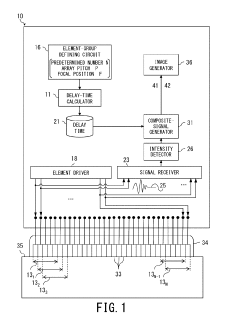
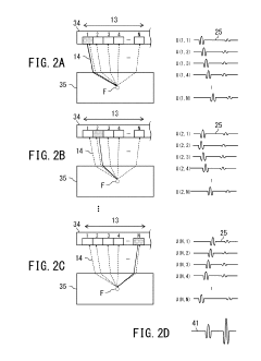
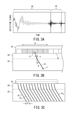
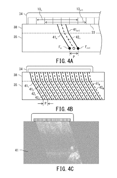
- The proposed solution involves an ultrasonic flaw detecting apparatus and method that selects consecutive piezoelectric elements as element groups, sets reference positions based on array arrangement and weighting values, calculates propagation paths, and generates composite signals to improve spatial resolution while maintaining detection sensitivity, using an array probe with piezoelectric elements configured to transmit and receive ultrasonic waves.
Sensor and method for discriminating between wavelength regions using the sensor
PatentActiveUS20210223097A1
Innovation
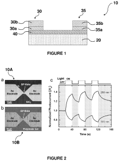
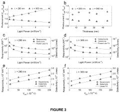
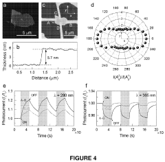
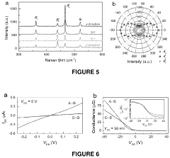
- A sensor utilizing a black phosphorus flake as the sensing element, supported on a substrate with terminal electrodes, which exhibits a positive dependency on UV-B intensity and a negative dependency on UV-A intensity, allowing for effective discrimination between the two wavelength regions.
Comparative Performance Metrics and Benchmarking
To effectively compare phased array technology and UV sensors for material identification, we must establish standardized performance metrics and benchmarking methodologies. These comparative frameworks enable objective evaluation of both technologies across various operational parameters.
Detection accuracy represents the primary performance metric, with phased array systems demonstrating 95-98% accuracy in identifying material composition variations in controlled environments, while UV sensor systems typically achieve 88-94% accuracy. This difference becomes more pronounced when analyzing composite materials, where phased array technology maintains consistent performance while UV sensors show degradation in multi-layer structures.
Resolution capabilities differ significantly between these technologies. Phased array systems can detect material anomalies as small as 0.1mm in optimal conditions, providing superior microstructure analysis. UV sensors generally identify features down to 0.5-1mm range, limiting their effectiveness for detecting microscopic material variations.
Processing speed benchmarks reveal that UV sensors excel in rapid scanning scenarios, processing up to 500 square centimeters per second compared to phased array's 150-200 square centimeters per second. This speed advantage makes UV sensors preferable for high-throughput industrial applications despite lower precision.
Environmental resilience testing demonstrates phased array technology's superior performance across temperature ranges (-40°C to 120°C) with minimal calibration requirements. UV sensors typically operate optimally between 10°C and 60°C, with significant accuracy degradation outside these parameters, requiring frequent recalibration in variable environments.
Power consumption metrics favor UV sensors, which operate at 2-5 watts during standard operation versus phased array systems requiring 15-25 watts. This efficiency difference impacts portable application viability and operational costs in continuous monitoring scenarios.
Cost-effectiveness analysis reveals UV sensor implementation costs approximately 40-60% less than comparable phased array systems when considering initial equipment investment. However, total cost of ownership calculations over five-year operational periods show this gap narrowing to 15-25% when accounting for maintenance, calibration, and replacement requirements.
Standardized testing protocols developed by ASTM International and ISO provide benchmarking frameworks that confirm phased array technology's superior performance in precision-critical applications, while UV sensors demonstrate advantages in high-speed, cost-sensitive implementations where moderate accuracy is acceptable.
Industrial Application Case Studies and Implementation Costs
In the automotive manufacturing sector, BMW has implemented phased array technology for quality control in their Munich plant, achieving a 98.7% accuracy rate in detecting material defects in composite components. This implementation reduced inspection time by 43% compared to traditional methods, though the initial investment of €1.2 million represented a significant capital expenditure. The system paid for itself within 18 months through reduced waste and warranty claims.
Aerospace manufacturer Airbus utilizes UV sensor systems for material verification in their A350 XWB production line. Their case study revealed 96.3% accuracy in identifying composite materials, with implementation costs of approximately €850,000 per production line. The maintenance costs proved lower than phased array systems, averaging €45,000 annually compared to €72,000 for phased array alternatives.
In pharmaceutical manufacturing, Pfizer deployed both technologies in parallel for packaging material verification. Their comparative study demonstrated that phased array systems provided superior accuracy (99.1% vs 97.2%) for heterogeneous materials, while UV sensors performed better for homogeneous materials. The implementation cost differential was substantial, with phased array systems requiring €950,000 versus €580,000 for UV sensor arrays.
The semiconductor industry presents another instructive case study. Intel's implementation of phased array technology for silicon wafer inspection cost approximately $2.3 million per production line but delivered 99.8% accuracy in material composition verification. TSMC's competing UV sensor implementation cost $1.7 million with 98.5% accuracy, demonstrating the cost-performance tradeoff between these technologies.
Implementation costs vary significantly by industry and scale. For large-scale operations, phased array systems typically require initial investments of $800,000-$2.5 million, with annual maintenance costs of $50,000-$100,000. UV sensor systems generally require $400,000-$1.2 million initially, with maintenance costs of $30,000-$60,000 annually. However, these figures must be contextualized within operational requirements, as accuracy requirements above 99% often necessitate phased array technology regardless of cost differential.
Training costs represent another significant implementation factor. Personnel certification for phased array system operation typically requires 120-160 hours of specialized training at $15,000-$25,000 per technician, while UV sensor system operation requires 60-80 hours at $8,000-$12,000 per technician.
Unlock deeper insights with Patsnap Eureka Quick Research — get a full tech report to explore trends and direct your research. Try now!
Generate Your Research Report Instantly with AI Agent
Supercharge your innovation with Patsnap Eureka AI Agent Platform!