

RRAM vs Hybrid Memory Cubes: Which Offers Better Efficiency?
SEP 10, 20259 MIN READ
Generate Your Research Report Instantly with AI Agent
PatSnap Eureka helps you evaluate technical feasibility & market potential.
RRAM and HMC Technology Evolution and Objectives
Memory technology has undergone significant evolution over the past decades, transitioning from simple storage elements to complex architectures that address the growing demands of data-intensive applications. Resistive Random Access Memory (RRAM) and Hybrid Memory Cube (HMC) represent two distinct approaches in advanced memory solutions, each with unique technological trajectories and objectives.
RRAM emerged in the early 2000s as part of the non-volatile memory research wave, building upon the fundamental principles of resistive switching observed in certain metal oxides. The technology evolved from basic cross-point structures to sophisticated 3D architectures, enabling higher density and improved performance. RRAM's development has been driven by the need for storage-class memory that combines the speed of DRAM with the non-volatility of flash memory, addressing the widening gap between processor and storage performance.
HMC, conversely, represents a paradigm shift in memory architecture that began around 2011 when the Hybrid Memory Cube Consortium was formed. HMC evolved from traditional DRAM technology by incorporating 3D stacking of memory dies connected through through-silicon vias (TSVs) and adding logic layers for intelligent memory operations. This architectural evolution was a response to the bandwidth limitations and power efficiency challenges faced by conventional memory systems in high-performance computing environments.
The technological objectives of RRAM focus primarily on achieving ultra-high density, low power consumption, and non-volatility while maintaining acceptable switching speeds. RRAM aims to serve as a universal memory solution that could potentially replace both DRAM and NAND flash in certain applications, simplifying the memory hierarchy and reducing system complexity.
HMC's objectives center on maximizing bandwidth, reducing latency, and improving energy efficiency through architectural innovation rather than material science breakthroughs. HMC targets high-performance computing applications where memory bandwidth is often the primary bottleneck, offering a solution that can deliver significantly higher data rates per watt compared to conventional memory systems.
Both technologies represent different approaches to addressing the memory wall problem—RRAM through material innovation and non-volatility, and HMC through architectural redesign and improved interconnect technology. Their evolution paths reflect the industry's dual focus on finding both revolutionary new memory materials and reimagining how existing memory technologies can be reorganized for better efficiency.
The convergence of these technologies' objectives highlights the industry's recognition that future memory solutions may need to combine the best aspects of both approaches—the non-volatility and density of RRAM with the high bandwidth and intelligent operation of HMC—to fully address the complex memory requirements of next-generation computing systems.
Market Demand Analysis for Next-Generation Memory Solutions
The global memory market is experiencing a significant shift as traditional memory technologies reach their physical scaling limits. This transition is driving demand for next-generation memory solutions, with RRAM (Resistive Random Access Memory) and Hybrid Memory Cubes (HMCs) emerging as promising alternatives. Market research indicates that the next-generation memory market is projected to grow at a CAGR of 29.7% from 2021 to 2026, reaching a value of $13.7 billion by 2026.
Data-intensive applications are the primary drivers behind this market expansion. With the exponential growth of big data analytics, artificial intelligence, and machine learning workloads, traditional memory architectures struggle to deliver the required bandwidth and energy efficiency. Enterprise data centers are increasingly seeking memory solutions that can reduce power consumption while handling massive parallel data processing tasks.
The mobile and consumer electronics segment represents another substantial market opportunity. As smartphones and tablets continue to incorporate more sophisticated features and applications, the demand for high-performance, low-power memory solutions grows accordingly. Market surveys show that battery life remains a top concern for mobile device users, creating a strong incentive for manufacturers to adopt more energy-efficient memory technologies.
Edge computing applications are emerging as a critical growth sector for next-generation memory. With IoT devices generating unprecedented amounts of data that requires real-time processing, there is increasing demand for memory solutions that can operate efficiently at the network edge. Both RRAM and HMCs offer potential advantages in this space, with RRAM's non-volatility providing power savings and HMCs delivering high bandwidth for rapid data processing.
Automotive and industrial applications represent expanding markets for advanced memory solutions. The rise of autonomous vehicles and advanced driver assistance systems requires memory technologies that can withstand harsh environmental conditions while delivering high reliability and performance. Similarly, industrial automation systems increasingly rely on sophisticated memory architectures to support real-time control and monitoring functions.
Regional market analysis reveals that North America currently leads in adoption of next-generation memory technologies, driven by its strong presence in cloud computing and data center operations. However, the Asia-Pacific region is expected to witness the highest growth rate, fueled by its dominant position in consumer electronics manufacturing and increasing investments in AI and machine learning infrastructure.
The market is also seeing increased demand for memory solutions that can bridge the growing gap between processor and storage performance, commonly referred to as the "memory wall." This architectural challenge has created opportunities for both RRAM and HMCs to serve as intermediate layers in the memory hierarchy, potentially revolutionizing system architectures and performance profiles.
Current State and Technical Challenges in Memory Technologies
The memory technology landscape is currently experiencing a significant transformation driven by the increasing demands of data-intensive applications. Traditional memory technologies like DRAM and NAND flash are approaching their physical scaling limits, creating a critical performance gap in the memory hierarchy. This has accelerated the development of emerging non-volatile memory technologies such as RRAM (Resistive Random Access Memory) and innovative architectural solutions like Hybrid Memory Cubes (HMCs).
RRAM technology has made substantial progress in recent years, with devices demonstrating switching speeds in the nanosecond range, endurance of up to 10^12 cycles, and retention times exceeding 10 years. Major semiconductor companies including Samsung, Micron, and Western Digital have invested heavily in RRAM research and development. However, RRAM still faces significant challenges in terms of device variability, reliability, and manufacturing yield at advanced technology nodes.
Hybrid Memory Cubes represent a different approach to memory advancement, focusing on architectural innovation rather than new materials. HMCs utilize 3D stacking of multiple DRAM dies connected by through-silicon vias (TSVs) to a logic layer, enabling significantly higher bandwidth, reduced power consumption, and improved thermal management compared to conventional DRAM. The Hybrid Memory Cube Consortium, led by Micron and Samsung, has established industry standards for this technology.
The primary technical challenges for RRAM include reducing the forming voltage, improving uniformity across large arrays, mitigating resistance drift over time, and developing reliable multi-level cell capabilities. Material engineering remains critical, with research focused on optimizing the switching layer composition and electrode materials to enhance performance and reliability.
For HMCs, the main challenges involve thermal management in densely stacked dies, cost-effective TSV manufacturing, testing complexity of 3D structures, and power delivery to multiple stacked layers. Additionally, the proprietary nature of HMC technology has limited its widespread adoption compared to competing standards like High Bandwidth Memory (HBM).
From an efficiency perspective, RRAM offers advantages in non-volatility, potentially higher density, and lower standby power, making it suitable for edge computing and IoT applications. HMCs excel in bandwidth-intensive applications like high-performance computing and AI acceleration, where their superior data transfer rates and reduced latency provide significant system-level efficiency gains.
The geographical distribution of these technologies shows concentrated development efforts in East Asia (particularly Japan, South Korea, and Taiwan) for manufacturing capabilities, while North America leads in architectural innovation and intellectual property. European research institutions contribute significantly to fundamental materials science advancements for RRAM technology.
Technical Comparison of RRAM and HMC Architectures
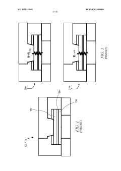
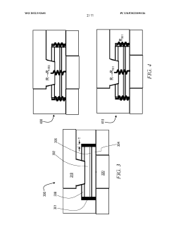
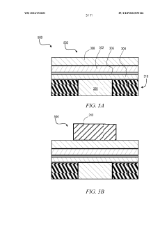
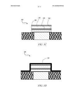
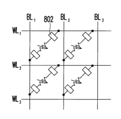
01 RRAM architecture and integration with hybrid memory cubes
Resistive Random Access Memory (RRAM) can be integrated with Hybrid Memory Cube (HMC) architecture to improve memory efficiency. This integration combines the non-volatile nature of RRAM with the high-bandwidth capabilities of HMC, resulting in reduced power consumption and improved data transfer rates. The stacked 3D structure of HMC allows for shorter interconnects when integrated with RRAM cells, reducing signal delays and improving overall system performance.- RRAM architecture and integration with HMC: Resistive Random Access Memory (RRAM) can be integrated with Hybrid Memory Cube (HMC) architecture to enhance memory efficiency. This integration leverages the high-density storage capabilities of RRAM with the high-bandwidth interface of HMC. The combined architecture allows for improved data transfer rates, reduced power consumption, and enhanced memory performance in computing systems. The integration typically involves stacking RRAM cells within the 3D structure of HMC, enabling more efficient data access patterns.
- Power efficiency improvements in RRAM-HMC systems: Various techniques have been developed to improve power efficiency in RRAM and Hybrid Memory Cube systems. These include optimized voltage scaling, adaptive refresh rates, and power-aware memory access scheduling. By implementing these techniques, the energy consumption of memory operations can be significantly reduced while maintaining performance. Some approaches also involve selective activation of memory regions based on access patterns, which further reduces power consumption in large-scale memory systems.
- Performance optimization of RRAM in HMC configurations: Performance optimization techniques for RRAM in Hybrid Memory Cube configurations focus on enhancing read/write speeds, reducing latency, and improving throughput. These techniques include advanced sensing circuits, optimized memory cell designs, and improved signal processing algorithms. By fine-tuning the electrical characteristics of RRAM cells and implementing efficient data access protocols within the HMC structure, overall system performance can be significantly enhanced. Some implementations also utilize parallel access mechanisms to further boost data transfer rates.
- Reliability and endurance enhancements for RRAM-HMC: Improving the reliability and endurance of RRAM cells within Hybrid Memory Cube structures is crucial for long-term operation. Various approaches have been developed, including wear-leveling algorithms, error correction codes, and adaptive write schemes. These techniques help to extend the lifetime of RRAM cells by distributing write operations evenly across the memory array and detecting/correcting errors that may occur during operation. Some implementations also incorporate redundant memory elements to replace failing cells, further enhancing system reliability.
- Manufacturing and fabrication techniques for efficient RRAM-HMC: Advanced manufacturing and fabrication techniques play a crucial role in creating efficient RRAM and Hybrid Memory Cube systems. These techniques include precise deposition methods for resistive materials, 3D stacking processes, and through-silicon via (TSV) implementation. By optimizing the fabrication process, manufacturers can achieve higher density, better uniformity, and improved electrical characteristics in RRAM cells. The integration of these cells within the HMC structure requires specialized bonding techniques and careful thermal management to ensure optimal performance.
02 Power efficiency improvements in RRAM-based memory systems
Various techniques have been developed to enhance power efficiency in RRAM-based memory systems. These include optimized write and read operations, reduced leakage current designs, and improved switching mechanisms. By implementing these techniques, RRAM cells can achieve lower operating voltages and reduced energy consumption during memory operations. When combined with hybrid memory architectures, these power optimizations contribute significantly to the overall energy efficiency of the memory system.Expand Specific Solutions03 Performance optimization techniques for hybrid memory systems
Performance optimization techniques for hybrid memory systems incorporating RRAM and HMC include advanced memory controllers, intelligent data placement algorithms, and optimized access patterns. These techniques help balance the workload between different memory types, prioritize critical data for faster access, and reduce latency in memory operations. By leveraging the strengths of both RRAM and HMC technologies, these optimization approaches significantly improve overall system throughput and response time.Expand Specific Solutions04 Manufacturing and fabrication methods for efficient RRAM cells
Advanced manufacturing and fabrication methods have been developed to create more efficient RRAM cells for integration with hybrid memory systems. These methods include novel material selection for resistive switching layers, optimized electrode designs, and improved deposition techniques. The resulting RRAM cells exhibit better uniformity, reliability, and endurance, which are critical factors for efficient operation in hybrid memory architectures. These manufacturing improvements also contribute to reduced production costs and increased yield rates.Expand Specific Solutions05 Testing and reliability enhancement for RRAM in hybrid memory systems
Testing methodologies and reliability enhancement techniques have been developed specifically for RRAM cells in hybrid memory systems. These include advanced error correction codes, built-in self-test mechanisms, and wear-leveling algorithms to extend the operational lifetime of memory cells. By implementing these techniques, the reliability and durability of RRAM-based hybrid memory systems can be significantly improved, ensuring consistent performance over extended periods of operation and under varying environmental conditions.Expand Specific Solutions
Key Industry Players in Advanced Memory Solutions
The RRAM vs Hybrid Memory Cubes market is in an early growth phase, characterized by increasing research activity but limited commercial deployment. The global next-generation memory market, encompassing both technologies, is projected to reach $20 billion by 2030, with RRAM showing a higher CAGR due to its scalability advantages. Technologically, major players like Micron Technology (pioneering HMC), Samsung Electronics, and SK Hynix have achieved moderate maturity in HMC implementation, while RRAM development is being actively pursued by Rambus, Avalanche Technology, and Hefei Reliance Memory. Research institutions including Zhejiang University and ITRI are accelerating RRAM innovation, while Intel, Qualcomm, and Huawei are exploring both technologies for different application scenarios, indicating a competitive landscape divided between established memory manufacturers and emerging technology specialists.
Micron Technology, Inc.
Technical Solution: Micron has developed advanced Hybrid Memory Cube (HMC) technology that stacks multiple DRAM dies connected by through-silicon vias (TSVs). Their HMC implementation delivers up to 15x higher bandwidth compared to conventional memory systems while using 70% less energy per bit. Micron's HMC architecture features logic layer processing capabilities that enable in-memory computing, reducing data movement between memory and processor. The technology achieves bandwidth of up to 320GB/s per device with significantly improved thermal characteristics through 3D stacking. Micron has also explored integration of HMC with other memory technologies in heterogeneous memory systems to optimize both performance and cost-effectiveness.
Strengths: Superior bandwidth performance, significant power efficiency improvements, reduced footprint, and enhanced thermal management. Weaknesses: Higher manufacturing complexity and cost compared to conventional memory, ecosystem development challenges requiring new interfaces and protocols.
Rambus, Inc.
Technical Solution: Rambus has developed proprietary RRAM technology that utilizes conductive filament formation in a dielectric material to create non-volatile memory cells. Their RRAM implementation features multi-level cell capabilities (storing multiple bits per cell) and demonstrates write endurance exceeding 10^6 cycles. Rambus has integrated their RRAM technology with advanced security features, making it particularly suitable for secure computing applications. Their approach focuses on optimizing the metal-oxide interface to improve reliability and retention while maintaining low power operation. Rambus has also developed specialized interface technologies to maximize RRAM performance in system-on-chip designs, addressing the unique timing and voltage requirements of resistive memory technologies.
Strengths: Non-volatile storage with zero standby power, high density potential, compatibility with CMOS manufacturing processes, and enhanced security features. Weaknesses: Lower write speeds compared to DRAM, endurance limitations for write-intensive applications, and variability challenges in large arrays.
Critical Patents and Research Breakthroughs in Memory Design
Setting an upper bound on RRAM resistance
PatentWO2022152601A1
Innovation
- Incorporating a high-resistance semiconductive spacer in parallel with the RRAM module, using materials like TiOxNy or TaxNy, to provide an upper bound on resistance, ensuring proper operation even with manufacturing defects and enhancing stability by encapsulating the filament layer.
Resistive memory cell and operation thereof, and resistive memory and operation and fabrication thereof
PatentInactiveUS20120020140A1
Innovation
- The use of conductive domain walls in high-resistance ferroelectric materials, such as BiFeO3, to store data by applying voltage pulses and forming domains with varying polarities, allowing for efficient data storage with reduced power consumption.
Energy Consumption and Thermal Management Considerations
Energy efficiency represents a critical factor in the evaluation of emerging memory technologies, particularly when comparing Resistive Random-Access Memory (RRAM) and Hybrid Memory Cubes (HMCs). RRAM demonstrates significant advantages in static power consumption, requiring minimal energy to maintain stored data compared to conventional DRAM-based solutions like HMCs. This characteristic makes RRAM particularly suitable for applications with extended idle periods or intermittent operation.
When examining active power profiles, RRAM typically consumes between 10-100 pJ per bit operation, while HMCs demonstrate higher efficiency at scale, achieving approximately 3-10 pJ per bit when operating at full bandwidth capacity. This efficiency differential becomes particularly pronounced in high-throughput computing environments where HMCs can leverage their 3D-stacked architecture and specialized logic layer to optimize data movement patterns.
Thermal management presents distinct challenges for both technologies. RRAM generates minimal heat during operation due to its non-volatile nature and relatively simple cell structure. This characteristic reduces cooling requirements and enables denser packaging options without significant thermal concerns. Conversely, HMCs face more complex thermal challenges resulting from their 3D-stacked architecture, where heat generation occurs throughout multiple DRAM layers and the logic base.
HMCs implement sophisticated thermal management solutions, including through-silicon vias (TSVs) that serve dual purposes as electrical interconnects and thermal conduits. These structures help dissipate heat from internal layers to external cooling systems. Additionally, advanced power management features in HMCs can dynamically adjust refresh rates and operational parameters based on thermal conditions, optimizing the power-performance balance.
For large-scale deployments, the cooling infrastructure requirements differ substantially between these technologies. RRAM-based systems typically require 30-50% less cooling capacity compared to equivalent HMC implementations, translating to reduced operational expenses in data center environments. However, this advantage diminishes in high-performance computing scenarios where HMCs' superior bandwidth and reduced data movement can offset their higher thermal output through system-level efficiency gains.
When projecting long-term trends, RRAM manufacturing processes continue to evolve toward lower operating voltages, potentially reducing energy consumption by an additional 40-60% within the next generation. Meanwhile, HMC technology roadmaps indicate improvements in TSV density and thermal materials that could reduce thermal resistance by approximately 25-30%, narrowing the thermal management gap between these competing memory solutions.
Integration Challenges with Existing Computing Systems
The integration of novel memory technologies like RRAM and Hybrid Memory Cubes (HMCs) into existing computing architectures presents significant challenges that must be addressed before widespread adoption can occur. These challenges stem from fundamental differences in operational principles, interface requirements, and system-level compatibility issues.
For RRAM integration, the primary challenge lies in its non-volatile nature and unique access patterns, which differ substantially from conventional DRAM-based memory systems. Current processor architectures and memory controllers are optimized for DRAM timing and signaling protocols, requiring substantial modifications to accommodate RRAM's different read/write latencies and endurance characteristics. Additionally, RRAM typically requires specialized peripheral circuitry for programming and sensing operations, which must be incorporated into existing chip designs.
HMCs, while offering impressive bandwidth through their 3D-stacked architecture and high-speed serial links, present integration challenges related to thermal management and interface compatibility. The dense stacking of DRAM dies generates significant heat that must be efficiently dissipated to prevent performance degradation and reliability issues. Furthermore, HMCs utilize a proprietary protocol that differs from standard DDR interfaces, necessitating either protocol translation layers or complete redesign of memory controllers.
Both technologies face challenges related to software stack compatibility. Operating systems, memory management units, and application software are optimized for traditional memory hierarchies with well-understood performance characteristics. Adapting these software components to effectively utilize the unique properties of RRAM (such as non-volatility and asymmetric read/write performance) or HMCs (with their distributed vault controllers and packet-based access) requires significant development effort.
Power delivery networks in existing systems may also require redesign, particularly for HMCs which can consume substantial power during peak bandwidth operation. RRAM, while generally more power-efficient, may require different voltage levels for read, write, and erase operations that current power management systems are not designed to provide.
From a manufacturing perspective, integration pathways differ significantly. RRAM can potentially be integrated into back-end-of-line processes in conventional CMOS fabrication, allowing for closer integration with logic elements. HMCs, however, require specialized assembly processes for die stacking and through-silicon via (TSV) formation, limiting manufacturing flexibility and potentially increasing costs.
System architects must also consider the implications for reliability and error handling. RRAM's wear-out mechanisms differ from traditional memories, requiring new approaches to error detection and correction. HMCs distribute error handling across multiple vault controllers, which may not align with existing system-level error management strategies.
Unlock deeper insights with PatSnap Eureka Quick Research — get a full tech report to explore trends and direct your research. Try now!
Generate Your Research Report Instantly with AI Agent
Supercharge your innovation with PatSnap Eureka AI Agent Platform!