

RRAM vs Optical Memories: Efficiency and Scalability
SEP 10, 20259 MIN READ
Generate Your Research Report Instantly with AI Agent
PatSnap Eureka helps you evaluate technical feasibility & market potential.
RRAM and Optical Memory Evolution and Objectives
Memory technologies have undergone significant evolution over the past decades, transitioning from magnetic storage to electronic memories and now exploring novel paradigms like resistive random-access memory (RRAM) and optical memories. RRAM emerged in the early 2000s as a promising non-volatile memory technology based on resistance switching phenomena in metal-oxide materials. Its development was driven by the increasing limitations of conventional flash memory in terms of scaling, power consumption, and endurance.
The evolution of RRAM has progressed through several generations, beginning with simple metal-oxide structures and advancing to sophisticated multi-layer architectures with enhanced reliability and performance characteristics. Early RRAM devices suffered from variability issues and limited endurance, but recent advancements have significantly improved these parameters, making RRAM a viable candidate for next-generation memory solutions.
Optical memory technologies have followed a parallel but distinct evolutionary path. Beginning with CD-ROMs in the 1980s and evolving through DVD and Blu-ray technologies, optical storage has traditionally focused on archival applications. However, recent breakthroughs in photonic materials and nanophotonics have opened new possibilities for high-speed, high-density optical memories that could potentially compete with electronic alternatives in certain applications.
The convergence of photonics and electronics has led to hybrid approaches that leverage the strengths of both domains. Photonic integrated circuits and silicon photonics have enabled new architectures for memory systems that combine the speed of light-based operations with the density advantages of electronic storage.
The primary objectives in comparing RRAM and optical memories center on addressing the growing challenges in computing systems. These include the memory wall problem (the widening gap between processor and memory speeds), energy efficiency concerns in data centers, and the need for storage solutions that can support emerging applications in artificial intelligence, edge computing, and the Internet of Things.
Specifically, researchers aim to determine which technology offers superior energy efficiency per bit operation, higher storage density, faster read/write speeds, better endurance, and longer retention times. Additionally, there is significant interest in understanding the scalability limitations of each technology and identifying potential pathways for overcoming these constraints.
The ultimate goal is to develop memory technologies that can meet the exponentially growing demands for data storage and processing while minimizing energy consumption and maximizing performance across diverse computing environments, from mobile devices to cloud infrastructure.
Market Demand Analysis for Next-Generation Memory Solutions
The memory technology market is experiencing a significant shift driven by the increasing demands of data-intensive applications such as artificial intelligence, machine learning, Internet of Things (IoT), and high-performance computing. Traditional memory technologies like DRAM and NAND flash are approaching their physical scaling limits, creating substantial market opportunities for next-generation memory solutions including Resistive Random-Access Memory (RRAM) and Optical Memories.
Market research indicates that the global next-generation memory market is projected to grow at a compound annual growth rate of over 40% through 2028, with the total addressable market expected to reach tens of billions of dollars. This explosive growth is primarily fueled by the exponential increase in data generation and processing requirements across various industries, particularly in cloud computing, edge computing, and autonomous systems.
RRAM technology has gained significant market traction due to its non-volatile nature, low power consumption, and compatibility with conventional CMOS fabrication processes. The demand for RRAM is particularly strong in embedded applications, IoT devices, and neuromorphic computing systems where energy efficiency is paramount. Industry analysts predict that RRAM could capture up to 15% of the specialty memory market within the next five years.
Optical memory technologies, while less commercially mature than RRAM, are attracting substantial interest due to their theoretical advantages in data transfer speeds, storage density, and energy efficiency. The market for optical storage solutions is expected to develop more rapidly in data center applications, where the benefits of high-bandwidth data transfer and potentially unlimited write endurance could provide significant competitive advantages.
Enterprise customers, particularly in financial services, healthcare, and telecommunications sectors, are expressing growing interest in next-generation memory solutions that can address the limitations of current technologies. These customers are willing to pay premium prices for memory solutions that offer substantial improvements in performance, energy efficiency, and reliability.
Consumer electronics manufacturers are also closely monitoring developments in both RRAM and optical memory technologies, with particular interest in solutions that can enable longer battery life, faster operation, and increased storage capacity in mobile and wearable devices. Market surveys indicate that consumers consistently rank battery life and device performance among their top purchasing considerations.
The automotive and industrial sectors represent emerging market opportunities for advanced memory technologies, driven by the increasing adoption of autonomous systems and industrial IoT applications. These sectors demand memory solutions with enhanced reliability, temperature stability, and radiation hardness – attributes that both RRAM and certain optical memory technologies can potentially deliver.
Technical Status and Barriers in Memory Technologies
Memory technologies have witnessed significant advancements in recent decades, yet continue to face substantial technical barriers that limit their efficiency and scalability. Current memory hierarchy implementations struggle to bridge the widening gap between processing speeds and memory access times, commonly referred to as the "memory wall." This fundamental challenge has driven research into alternative memory technologies beyond traditional DRAM and NAND flash.
Resistive Random-Access Memory (RRAM) has emerged as a promising non-volatile memory technology, offering theoretical advantages in density, power consumption, and switching speed. However, RRAM faces critical technical barriers including resistance drift, limited endurance cycles (typically 10^6-10^9 compared to DRAM's 10^15), and challenges in multi-level cell implementation. Material stability issues and sneak path currents in crossbar arrays further complicate large-scale deployment.
Optical memories represent another frontier, utilizing photons rather than electrons for data storage and retrieval. These technologies promise exceptional bandwidth potential and reduced power consumption for data transmission. Current implementations include holographic storage and photonic crystals. Despite theoretical advantages, optical memories face significant barriers in miniaturization, with diffraction limits constraining storage density. Integration with conventional electronic systems remains complex, requiring specialized optical-electronic interfaces that add latency and energy overhead.
Both technologies encounter manufacturing scalability challenges. RRAM fabrication processes require precise control of nanoscale structures and material compositions, leading to yield issues at advanced nodes. Optical memories demand specialized materials and precise alignment systems that are difficult to integrate into standard semiconductor manufacturing flows.
Energy efficiency presents another critical consideration. While RRAM offers lower operational power than conventional memories, its write operations remain energy-intensive. Optical memories demonstrate excellent energy efficiency during data transmission but require energy-consuming conversions between optical and electronic domains.
The thermal management of these technologies differs substantially. RRAM generates significant heat during switching operations, necessitating advanced cooling solutions at high densities. Optical memories produce less operational heat but may require temperature-stabilized environments to maintain reliable operation of sensitive optical components.
Reliability metrics also vary considerably. RRAM suffers from retention degradation at elevated temperatures and exhibits variability in switching behavior. Optical memories demonstrate excellent data retention characteristics but may be susceptible to mechanical disturbances and material degradation over time.
These technical barriers have limited widespread commercial adoption despite decades of research investment. The path forward requires interdisciplinary approaches combining materials science, device physics, circuit design, and system architecture to overcome these fundamental challenges.
Current Technical Approaches for Memory Efficiency
01 RRAM device structures and materials for improved efficiency
Resistive Random Access Memory (RRAM) devices can be designed with specific materials and structures to enhance efficiency and scalability. These designs include optimized electrode materials, resistive switching layers, and novel cell architectures that improve power consumption, switching speed, and reliability. Advanced materials such as metal oxides and specialized doping techniques can significantly enhance the performance characteristics of RRAM devices while maintaining their scalability advantages.- RRAM Device Structure and Materials: Resistive Random Access Memory (RRAM) devices utilize specific material compositions and structural designs to enhance efficiency and scalability. These devices typically employ metal oxide layers as the resistive switching material, with various electrode configurations to control the formation and rupture of conductive filaments. Advanced material engineering, including doping and interface optimization, allows for improved switching characteristics, reduced power consumption, and enhanced endurance. The structural design focuses on minimizing cell size while maintaining reliable operation, contributing to higher density memory arrays.
- Optical Memory Technologies and Integration: Optical memory systems utilize light for data storage and retrieval, offering advantages in bandwidth and energy efficiency. These technologies incorporate photonic structures, phase-change materials, and specialized waveguides to manipulate light signals for memory operations. Integration approaches combine optical elements with electronic control circuitry to create hybrid memory systems that leverage the strengths of both domains. Advanced fabrication techniques enable the miniaturization of optical components while maintaining high performance, addressing challenges in thermal management and signal integrity for scaled implementations.
- Scaling Techniques for Memory Density: Various scaling techniques are employed to increase memory density while maintaining or improving performance metrics. These include 3D stacking architectures, cross-point array configurations, and selector device integration to minimize sneak path currents. Advanced lithography and etching processes enable the fabrication of smaller feature sizes, while novel cell designs reduce the footprint of individual memory elements. Scaling strategies also address challenges related to thermal crosstalk, signal integrity, and power distribution in high-density memory arrays, ensuring reliable operation as dimensions decrease.
- Energy Efficiency Optimization: Energy efficiency in memory technologies is optimized through various approaches including low-voltage operation, improved switching materials, and intelligent power management schemes. Circuit-level innovations reduce the energy required for read and write operations, while architectural enhancements minimize standby power consumption. Pulse engineering techniques optimize the duration and amplitude of programming signals to achieve reliable switching with minimal energy expenditure. These optimizations are crucial for applications with strict power constraints, such as mobile devices and IoT systems, where battery life and thermal management are critical considerations.
- Hybrid and Multi-functional Memory Systems: Hybrid memory systems combine different memory technologies to leverage their complementary strengths, creating solutions with enhanced performance, efficiency, and scalability. These systems may integrate RRAM with optical elements, conventional CMOS, or other emerging memory technologies. Multi-functional memory architectures enable in-memory computing capabilities, where data processing occurs within the memory array, reducing energy-intensive data movement. Advanced control schemes coordinate the operation of heterogeneous memory components, optimizing for specific workloads while maintaining system-level efficiency and reliability across varying operating conditions.
02 Optical memory technologies for high-density data storage
Optical memory technologies offer unique advantages for high-density data storage applications. These systems utilize light for reading and writing data, enabling higher storage densities compared to conventional electronic memories. Advanced optical memory designs incorporate novel materials, wavelength optimization, and specialized recording techniques to improve data retention, access speeds, and energy efficiency. These technologies are particularly valuable for applications requiring massive data storage with reasonable access times.Expand Specific Solutions03 Integration and scaling techniques for memory technologies
Various integration and scaling techniques have been developed to enhance the efficiency and density of both RRAM and optical memory technologies. These include 3D stacking architectures, cross-point array structures, and advanced lithography methods that enable higher memory densities while maintaining performance. Specialized fabrication processes and design rules help overcome scaling challenges related to interference, power consumption, and reliability as device dimensions shrink to nanometer scales.Expand Specific Solutions04 Hybrid memory systems combining RRAM and optical technologies
Hybrid memory systems that combine the advantages of both RRAM and optical memory technologies can offer superior performance characteristics. These systems leverage the high speed and low power consumption of RRAM with the high storage density of optical memories. Integration approaches include specialized interfaces, data management algorithms, and hierarchical storage architectures that optimize overall system efficiency. Such hybrid solutions can address diverse application requirements ranging from high-performance computing to large-scale data centers.Expand Specific Solutions05 Advanced control and operation methods for memory efficiency
Advanced control and operation methods significantly improve the efficiency and reliability of both RRAM and optical memory technologies. These include specialized programming algorithms, error correction techniques, and intelligent power management systems that optimize performance while minimizing energy consumption. Novel read/write schemes, pulse shaping techniques, and adaptive control mechanisms help extend device lifetimes, improve data retention, and enhance overall system reliability while maintaining compatibility with existing memory hierarchies.Expand Specific Solutions
Key Industry Players in Advanced Memory Development
The RRAM vs Optical Memories competition is currently in an early growth phase, with the market expected to expand significantly as these technologies mature. RRAM offers superior scalability and energy efficiency compared to traditional memories, while optical memories provide advantages in data transfer speeds. The global market for these next-generation memory technologies is projected to reach several billion dollars by 2025. Among key players, Samsung, Intel, and TSMC lead in manufacturing capabilities, while specialized companies like Everspin Technologies and Unity Semiconductor focus on RRAM innovation. Research institutions including CEA and Industrial Technology Research Institute contribute significant advancements. Companies like Fujitsu and Sony are developing hybrid solutions that leverage both technologies' strengths, indicating a trend toward complementary rather than purely competitive development paths.
Samsung Electronics Co., Ltd.
Technical Solution: Samsung has developed advanced RRAM technology based on their proprietary 3D stacking architecture. Their solution integrates RRAM cells in a cross-point array structure with selector devices to minimize sneak path currents, achieving high density memory arrays. Samsung's RRAM technology demonstrates switching speeds of less than 10ns, endurance of over 10^6 cycles, and retention times exceeding 10 years at 85°C. For optical memories, Samsung has invested in holographic storage technology with volumetric data storage capabilities reaching theoretical densities of 1TB/cm³. Their dual approach allows them to leverage the strengths of both technologies depending on application requirements, with RRAM targeted at embedded applications and optical solutions for archival storage.
Strengths: Vertical integration capabilities allow Samsung to optimize both memory technologies and supporting hardware; extensive manufacturing infrastructure enables rapid scaling. Weaknesses: Their RRAM technology still faces challenges with variability in resistance states and requires relatively high operating voltages compared to conventional memories.
Unity Semiconductor Corp.
Technical Solution: Unity Semiconductor has pioneered CMOx (Conductive Metal Oxide) technology, a unique form of RRAM that utilizes ionic movement in metal oxides to create multiple resistance states. Their multi-layer cross-point architecture enables 3D stacking of memory cells without requiring a transistor at each cell, significantly increasing density while reducing manufacturing complexity. Unity's RRAM solution achieves write speeds of approximately 20ns, read speeds of 5ns, and demonstrates a 4x density advantage over conventional NAND flash. Their technology employs a proprietary selector device that effectively eliminates cross-talk between cells while maintaining low power operation. Unity has focused exclusively on RRAM development rather than optical memories, positioning their technology as an ideal solution for storage-class memory applications that bridge the performance gap between DRAM and NAND flash.
Strengths: Specialized focus on RRAM technology has resulted in advanced materials engineering and innovative cell architecture; their multi-level cell capability enables higher bit density per cell. Weaknesses: As a smaller company with limited manufacturing capacity, Unity faces challenges in scaling production to compete with larger semiconductor manufacturers; their exclusive focus on RRAM means they lack diversification into optical memory technologies.
Critical Patents and Innovations in Memory Architecture
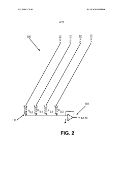
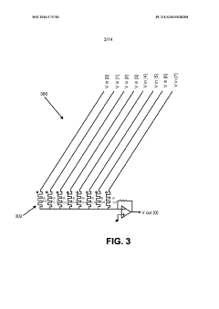
Resistive random-access memory array with reduced switching resistance variability
PatentInactiveUS20190371857A1
Innovation
- The fabrication of RRAM memory cells comprising multiple parallel-connected resistive memory devices, where each cell shares a common horizontal electrode layer, effectively averaging the switching resistances to minimize variability and noise.


Discrete-time analog filtering
PatentWO2016175781A1
Innovation
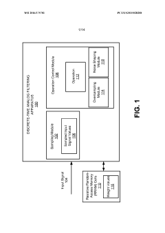
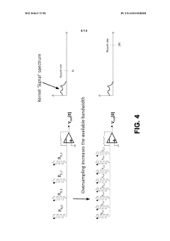
- A discrete-time analog filtering apparatus and method using oversampling and noise shaping to improve accuracy in RRAM cells, where the apparatus includes a sampling module, an operation control module with oversampling and noise shaping capabilities, to efficiently perform Multiply-Accumulate operations and retain accuracy in computations by displacing quantization noise from the baseband into a wider bandwidth.
Energy Consumption Comparison and Optimization
Energy consumption represents a critical factor in the evaluation of memory technologies, particularly when comparing RRAM (Resistive Random Access Memory) and optical memory systems. RRAM technologies typically operate on the principle of resistance switching, consuming energy primarily during write operations when structural changes occur within the resistive material. Current RRAM implementations demonstrate power consumption in the range of 0.1-10 pJ per bit for write operations, while read operations consume significantly less, approximately 0.01-1 pJ per bit.
Optical memories, conversely, utilize photons rather than electrons for data storage and retrieval. This fundamental difference results in distinct energy consumption patterns. Phase-change optical memories require substantial energy for the phase transition process during writing, typically consuming 10-100 pJ per bit. However, they excel in read operations, which can be performed with minimal energy expenditure, often below 0.1 pJ per bit when utilizing efficient laser sources.
The energy efficiency comparison reveals interesting trade-offs between these technologies. RRAM demonstrates superior overall energy efficiency in write-intensive applications, particularly in scenarios requiring frequent data modifications. The localized resistance changes in RRAM require minimal energy to maintain state, resulting in negligible standby power consumption. This characteristic makes RRAM particularly attractive for edge computing and IoT applications where power constraints are significant.
Optimization strategies for RRAM energy consumption focus on material engineering and circuit design. Recent advancements in hafnium oxide-based RRAM have reduced switching energy by up to 40% compared to earlier generations. Additionally, innovative pulse-shaping techniques during write operations have demonstrated potential energy savings of 25-35% without compromising data retention or endurance.
For optical memories, energy optimization efforts concentrate on improving the efficiency of light sources and detectors. The development of vertical-cavity surface-emitting lasers (VCSELs) with enhanced wall-plug efficiency has reduced the energy cost of optical writing operations. Furthermore, wavelength-division multiplexing techniques enable parallel operations, effectively amortizing the energy cost across multiple bits and improving overall efficiency.
Scaling considerations significantly impact energy consumption profiles. As RRAM cells shrink below 10nm, quantum effects and increased leakage currents pose challenges to energy efficiency. Conversely, optical memories face diffraction limits that constrain miniaturization but benefit from reduced crosstalk and interference at larger feature sizes, potentially offering more predictable energy consumption characteristics at scale.
Manufacturing Challenges and Process Integration
Manufacturing RRAM devices presents significant integration challenges compared to optical memory technologies. RRAM fabrication requires precise control of nanoscale structures and material interfaces, with critical dimensions often below 20nm. The deposition of switching materials like metal oxides (HfOx, TaOx) demands atomic-level precision to ensure consistent resistive switching behavior. Variations in film thickness of even 1-2nm can dramatically alter device performance characteristics, creating yield and reliability issues that impact mass production feasibility.
Process integration for RRAM involves complex compatibility issues with standard CMOS processes. The high temperatures required for certain RRAM material deposition and annealing steps (often exceeding 400°C) can compromise previously fabricated CMOS components. Additionally, metal contamination from RRAM materials can potentially diffuse into adjacent structures, necessitating specialized barrier layers that add manufacturing complexity and cost.
Optical memories, particularly those based on phase-change materials, face different manufacturing challenges. While they benefit from established optical storage manufacturing infrastructure, scaling to higher densities requires overcoming the diffraction limit through near-field techniques or plasmonic structures. The precision required for fabricating nanophotonic components with feature sizes below 100nm presents significant lithography and etching challenges.
3D integration represents a critical manufacturing consideration for both technologies. RRAM has demonstrated promising results in crossbar architectures and 3D stacking, but faces challenges in vertical interconnect uniformity and thermal management during operation. Each additional layer compounds manufacturing complexity and potential defect rates. Optical memories require precise alignment of optical components in three dimensions, with alignment tolerances often below 50nm to maintain proper light coupling and signal integrity.
Yield management differs substantially between these technologies. RRAM suffers from intrinsic variability in switching behavior, requiring sophisticated error correction and redundancy schemes. Manufacturing processes must incorporate extensive testing and binning procedures. Optical memories generally demonstrate better uniformity in manufacturing but are more sensitive to surface defects and contamination that can scatter light and degrade signal quality.
Cost considerations ultimately determine industrial adoption. Current RRAM manufacturing requires specialized equipment for precise material deposition and characterization, though it leverages many existing semiconductor manufacturing tools. Optical memories benefit from established manufacturing infrastructure but require specialized optical components that may limit cost reduction pathways as dimensions shrink below current optical storage norms.
Unlock deeper insights with PatSnap Eureka Quick Research — get a full tech report to explore trends and direct your research. Try now!
Generate Your Research Report Instantly with AI Agent
Supercharge your innovation with PatSnap Eureka AI Agent Platform!