RRAM vs Spintronics: Power Efficiency and Application Fit
SEP 10, 20259 MIN READ
Generate Your Research Report Instantly with AI Agent
PatSnap Eureka helps you evaluate technical feasibility & market potential.
RRAM and Spintronics Evolution and Objectives
Resistive Random Access Memory (RRAM) and Spintronics represent two significant paradigm shifts in memory and computing technologies that have evolved over distinct timelines. RRAM emerged in the early 2000s as researchers sought alternatives to conventional charge-based memory technologies. The fundamental concept of RRAM—utilizing resistance changes in dielectric materials to store information—can be traced back to the 1960s, but practical implementations only gained momentum in the past two decades with advancements in material science and nanofabrication techniques.
The evolution of RRAM has progressed through several generations, beginning with simple metal-insulator-metal structures and advancing to complex multi-layer architectures incorporating various oxide materials such as HfOx, TaOx, and TiOx. This progression has been driven by the need to address initial challenges related to reliability, endurance, and switching uniformity.
Spintronics, meanwhile, has followed a different evolutionary path since its conceptual foundation in the 1980s. The discovery of giant magnetoresistance (GMR) in 1988 by Albert Fert and Peter Grünberg—later awarded the Nobel Prize—marked the first major milestone. This was followed by the development of tunnel magnetoresistance (TMR) and magnetic tunnel junctions (MTJs), which form the basis of modern spintronic devices.
The technological objectives for both RRAM and Spintronics have converged around several key parameters: power efficiency, scalability, speed, endurance, and integration capability with conventional CMOS technology. Power efficiency has become particularly critical as computing systems face increasing energy constraints, with both technologies promising significant improvements over traditional memory solutions.
For RRAM, the primary objectives include reducing operating voltages below 1V, achieving switching speeds comparable to DRAM (<10ns), extending endurance beyond 10^12 cycles, and maintaining data retention for over 10 years at elevated temperatures. Additionally, there is a strong focus on multi-level cell capabilities to increase storage density.
Spintronics technology aims to leverage the inherent non-volatility of magnetic storage while achieving SRAM-like performance. Key objectives include reducing critical switching current density, improving thermal stability, enhancing TMR ratio for better readability, and developing materials compatible with back-end-of-line processes in semiconductor manufacturing.
Both technologies are now evolving toward neuromorphic computing applications, where their analog characteristics can be exploited for implementing artificial neural networks. This represents a significant shift from merely serving as memory elements to becoming computational units in their own right, potentially revolutionizing the traditional von Neumann computing architecture.
Market Demand Analysis for Low-Power Memory Technologies
The global memory technology market is experiencing a significant shift towards low-power solutions, driven primarily by the explosive growth of mobile devices, Internet of Things (IoT) applications, and edge computing systems. Current projections indicate the low-power memory market will reach approximately $12 billion by 2026, with a compound annual growth rate exceeding 14% between 2021 and 2026.
This accelerated growth stems from several converging market demands. First, the proliferation of battery-powered devices necessitates memory technologies that can operate efficiently within strict power budgets. Smartphone manufacturers are particularly vocal about this need, as memory operations can account for up to 25% of a mobile device's power consumption.
The IoT sector represents another substantial market driver, with an estimated 75 billion connected devices expected by 2025. These devices typically operate in power-constrained environments, often relying on energy harvesting or small batteries with multi-year life requirements. This creates an urgent demand for memory solutions that can function at sub-milliwatt power levels while maintaining data integrity.
Data centers and cloud infrastructure providers constitute a third significant market segment. With data centers currently consuming approximately 1-2% of global electricity, there is mounting pressure to reduce operational costs and carbon footprints. Memory subsystems account for roughly 30-40% of server power consumption, making low-power memory technologies particularly attractive for these applications.
Industry surveys indicate that system designers prioritize several key attributes when selecting memory technologies: power efficiency during both active and standby states, data retention without power (non-volatility), cost per bit, and integration compatibility with existing manufacturing processes. Both RRAM and spintronics address these requirements differently, creating distinct market opportunities.
Geographically, North America and Asia-Pacific regions dominate the demand landscape. North America leads in research funding and early adoption, while Asia-Pacific demonstrates the highest growth rate due to its manufacturing capacity and expanding consumer electronics markets. European demand centers primarily around industrial applications and automotive systems.
The automotive sector represents an emerging high-value market segment, with advanced driver assistance systems and autonomous vehicles requiring memory solutions that can operate reliably in extreme conditions while maintaining ultra-low power profiles. This segment is projected to grow at nearly 20% annually through 2026.
Customer interviews reveal that while cost remains important, many applications are increasingly willing to pay premium prices for memory technologies that deliver substantial power savings, particularly when total system power budgets and battery life are critical differentiators in end products.
Current State and Technical Barriers in Non-Volatile Memory
Non-volatile memory (NVM) technologies have evolved significantly over the past decade, with RRAM (Resistive Random Access Memory) and Spintronics emerging as promising alternatives to traditional flash memory. Currently, the NVM landscape is dominated by NAND and NOR flash technologies, which face inherent scaling limitations below 10nm node due to charge leakage issues and reliability concerns.
RRAM technology has reached commercial maturity in select applications, with companies like Crossbar and Weebit Nano demonstrating working prototypes and limited production. RRAM offers advantages in switching speed (10-100ns) and endurance (10^6-10^9 cycles), but faces challenges in resistance drift over time and variability between cells. The current density requirements for reliable switching operations remain a significant barrier to further power efficiency improvements.
Spintronics-based memories, particularly STT-MRAM (Spin-Transfer Torque Magnetic RAM), have seen accelerated development with companies like Everspin and Samsung introducing commercial products. These technologies leverage electron spin rather than charge, offering theoretical advantages in power consumption during standby operations. However, the write energy remains relatively high compared to ideal targets, with current densities of 0.5-1 MA/cm² still required for reliable switching.
A critical technical barrier for both technologies is the power-performance trade-off. RRAM exhibits excellent scalability but suffers from relatively high operating voltages (1.5-3V) compared to CMOS logic levels. Spintronics offers non-volatility with virtually unlimited endurance but requires significant current for write operations, limiting its application in ultra-low-power scenarios.
Material stability presents another significant challenge. RRAM relies on controlled defect migration in oxide materials, which can be affected by temperature variations and manufacturing inconsistencies. Spintronics technologies face challenges in thermal stability of magnetic materials, particularly as device dimensions shrink below 20nm.
Integration with CMOS processes represents a substantial hurdle for widespread adoption. While RRAM benefits from relatively simple fabrication requirements, achieving consistent electrical characteristics across large arrays remains problematic. Spintronics technologies require specialized materials and precise layer deposition techniques that are not standard in conventional semiconductor manufacturing.
From an application perspective, RRAM currently shows advantages in storage-class memory applications where density is prioritized, while Spintronics demonstrates better performance in cache-replacement scenarios where speed and endurance are critical. The geographical distribution of technical expertise shows concentration in East Asia for manufacturing optimization, while North America leads in fundamental materials research and novel architecture development.
Comparative Analysis of RRAM and Spintronics Solutions
01 Low-power RRAM device structures
Resistive Random Access Memory (RRAM) devices can be designed with specific structures to enhance power efficiency. These structures include optimized electrode materials, resistive switching layers, and interface engineering techniques. By carefully selecting materials and designing the device architecture, power consumption during read and write operations can be significantly reduced while maintaining reliable data storage capabilities.- Low-power RRAM device structures: Resistive Random Access Memory (RRAM) devices can be designed with specific structures to enhance power efficiency. These structures include optimized electrode materials, resistive switching layers, and interface engineering techniques that reduce the energy required for switching operations. By carefully controlling the device geometry and material composition, power consumption during write and read operations can be significantly reduced while maintaining reliable data storage capabilities.
- Spintronics-based memory power optimization: Spintronic memory technologies utilize electron spin rather than charge for data storage, offering inherent power advantages. These devices can be optimized through magnetic material selection, spin-transfer torque mechanisms, and perpendicular magnetic anisotropy to reduce switching currents. Advanced spintronic memory designs incorporate tunnel magnetoresistance effects and spin-orbit coupling to achieve non-volatile storage with minimal energy consumption during both standby and active operations.
- Hybrid RRAM-spintronic architectures: Combining RRAM and spintronic technologies creates hybrid memory architectures that leverage the advantages of both approaches. These hybrid systems can utilize RRAM for high-density storage while employing spintronic elements for logic operations or as selector devices. The integration enables reduced power consumption through optimized data paths, shared sensing circuits, and complementary switching mechanisms that minimize overall system energy requirements while maintaining performance metrics.
- Circuit-level power efficiency techniques: Power efficiency in RRAM and spintronic systems can be enhanced through specialized circuit designs. These include low-voltage sensing amplifiers, energy-recovery write drivers, and adaptive biasing schemes that minimize static power consumption. Advanced circuit techniques such as pulse-width modulation, current-limiting structures, and multi-level sensing approaches further reduce the energy required for memory operations while maintaining reliability and performance across varying operating conditions.
- System-level power management for emerging memories: System-level approaches to power management for RRAM and spintronic technologies involve comprehensive strategies across the memory hierarchy. These include power-aware memory controllers, dynamic voltage and frequency scaling, selective activation of memory arrays, and intelligent data placement algorithms. By implementing sleep modes, refresh rate optimization, and workload-adaptive operation policies, these systems can significantly reduce overall power consumption while maintaining the performance benefits of non-volatile memory technologies.
02 Spintronics-based memory power optimization
Spintronics technology leverages electron spin properties to create energy-efficient memory devices. By utilizing magnetic tunnel junctions (MTJs) and spin-transfer torque mechanisms, these devices can achieve lower power consumption compared to conventional memory technologies. Advanced materials and structures in spintronic devices enable non-volatile storage with minimal standby power and reduced switching energy requirements.Expand Specific Solutions03 Hybrid RRAM-spintronic architectures
Combining RRAM and spintronics technologies creates hybrid memory architectures with enhanced power efficiency. These hybrid systems leverage the complementary advantages of both technologies, such as the high density of RRAM and the low switching energy of spintronic elements. Integration techniques include shared control circuitry, optimized addressing schemes, and novel interconnect designs that minimize energy losses during data transfer operations.Expand Specific Solutions04 Circuit-level power management techniques
Power efficiency in RRAM and spintronic systems can be improved through specialized circuit designs. These include adaptive voltage scaling, pulse-width modulation for write operations, and sense amplifier optimizations for read operations. Advanced power gating techniques, leakage current reduction methods, and energy-recovery circuits further enhance the overall power efficiency of memory subsystems based on these technologies.Expand Specific Solutions05 System-level integration for energy efficiency
System-level approaches to integrating RRAM and spintronic technologies focus on optimizing the entire memory hierarchy for power efficiency. These approaches include intelligent data placement algorithms, power-aware memory controllers, and dynamic reconfiguration capabilities. By coordinating memory access patterns and implementing workload-specific optimizations, these systems can significantly reduce energy consumption while maintaining or improving performance metrics.Expand Specific Solutions
Key Industry Players and Competitive Landscape
The RRAM vs Spintronics competitive landscape is currently in an early growth phase, with the market expected to expand significantly as these technologies mature. RRAM offers advantages in power efficiency for certain applications, while Spintronics shows promise for high-performance computing scenarios. Key players like Intel, Samsung, and IBM are investing heavily in both technologies, with specialized companies like Everspin Technologies focusing exclusively on Spintronics (MRAM). TSMC and GLOBALFOUNDRIES are developing manufacturing capabilities, while research institutions including Max Planck Society and ITRI are advancing fundamental science. The technology maturity varies, with RRAM closer to widespread commercial deployment, while Spintronics requires further development despite offering potentially superior long-term power efficiency for specific applications.
Intel Corp.
Technical Solution: Intel has developed 3D XPoint memory technology (a form of RRAM) in collaboration with Micron, featuring cross-point architecture that enables high density storage with cell sizes approaching 4F². Their RRAM implementation demonstrates read latencies of approximately 100ns and write latencies of 500ns, with power consumption in the range of 25-100 pJ per bit operation. Intel's RRAM technology operates at voltages below 3V with programming currents in the microamp range, significantly reducing power requirements compared to conventional flash memory. For spintronics, Intel has invested in Spin-Transfer Torque MRAM (STT-MRAM) research, achieving devices with thermal stability factors exceeding 60 (enabling 10-year data retention) while maintaining switching energies below 200 pJ per bit. Their comparative analysis shows RRAM excelling in density and multi-level cell capability, while spintronics offers superior endurance (>10^12 vs 10^6-10^9 cycles for RRAM) and faster switching speeds. Intel has also explored hybrid memory systems that leverage both technologies, using MRAM for cache levels and RRAM for higher density storage tiers.
Intel's RRAM technology offers exceptional density and non-volatility with zero standby power, making it ideal for data center storage and persistent memory applications. Their spintronics solutions provide better endurance and faster switching speeds, suitable for cache replacement. However, RRAM still faces challenges with resistance drift over time affecting long-term reliability, while their spintronic devices require higher write currents, limiting their application in ultra-low-power scenarios.
Samsung Electronics Co., Ltd.
Technical Solution: Samsung has developed advanced RRAM technology utilizing transition metal oxides (particularly HfO2-based compounds) that demonstrate switching voltages below 3V and programming currents in the microamp range. Their RRAM cells achieve power consumption of approximately 10-100 pJ per operation with data retention exceeding 10 years at 85°C. Samsung's RRAM architecture incorporates innovative selector devices to minimize sneak path currents in crossbar arrays, significantly reducing standby power consumption. In parallel, Samsung has invested heavily in spintronics research, developing Spin-Transfer Torque MRAM (STT-MRAM) with perpendicular magnetic anisotropy that reduces switching current by approximately 50% compared to in-plane magnetization designs. Their STT-MRAM cells operate with write energies of 100-200 pJ per bit and read energies below 10 pJ. Samsung has conducted extensive comparative analysis between these technologies, finding RRAM superior for high-density storage applications (with cell sizes approaching 4F²) while their spintronics solutions offer better endurance (>10^12 cycles) and faster switching speeds (1-10ns).
Samsung's RRAM technology offers superior density and multi-level cell capability, making it ideal for mass storage applications. Their spintronics solutions provide better endurance and radiation hardness, suitable for automotive and aerospace applications. However, RRAM faces challenges with resistance drift and variability, while their spintronic devices require more complex fabrication processes and have higher write energy requirements.
Core Patents and Technical Innovations in Memory Technologies
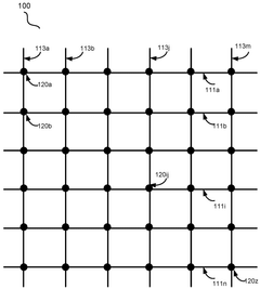
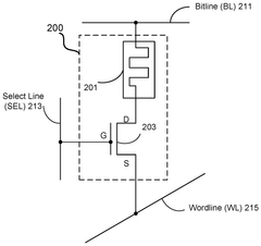
Resistive random-access memory (RRAM) devices with interface layers
PatentWO2024259355A2
Innovation
- The introduction of an interface layer with a discontinuous dielectric material and conductive particles between the electrode and the switching oxide layer, which reduces the filament size by channeling electric fields and currents through conductive particles, thereby decreasing the forming and switching voltages.
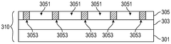
Resistive random access memory and manufacturing method thereof
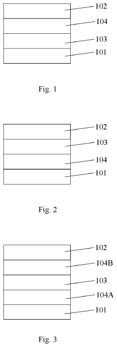
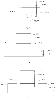
PatentActiveUS20210028358A1
Innovation
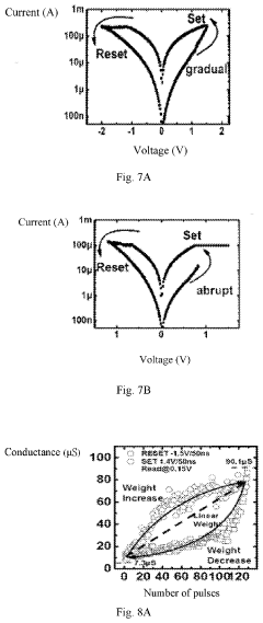
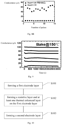
- Incorporating a thermal enhanced layer with lower thermal conductivity than the electrodes, positioned adjacent to the resistive layer, to slow down heat loss and promote the formation of dispersed conductive filaments, allowing continuous and bidirectional linear changes in conductance.
Energy Efficiency Metrics and Benchmarking Methodologies
To effectively compare and evaluate the power efficiency of RRAM and spintronics technologies, standardized metrics and benchmarking methodologies are essential. The energy consumption per operation serves as a fundamental metric, typically measured in femtojoules (fJ) or picojoules (pJ) per bit. For RRAM, this encompasses the energy required for SET/RESET operations, while for spintronics, it includes the energy needed for magnetization switching or domain wall movement.
Static power consumption represents another critical parameter, measuring leakage current during idle states. RRAM generally exhibits lower leakage compared to conventional CMOS, while spintronics demonstrates near-zero static power consumption due to its non-volatile nature, providing a significant advantage in energy-constrained applications.
Energy-delay product (EDP) offers a comprehensive metric that balances performance with energy efficiency. This metric is particularly valuable when comparing technologies with different speed-power tradeoffs, as RRAM typically offers moderate switching speeds with low power, while certain spintronic implementations may deliver faster operation at higher instantaneous power.
Benchmarking methodologies must account for application-specific workloads to provide meaningful comparisons. Memory-intensive workloads that emphasize frequent read/write operations highlight different efficiency aspects compared to compute-in-memory applications. Standardized benchmarks such as SPEC CPU for processor-centric evaluations or MLPerf for machine learning applications provide consistent frameworks for comparison.
Temperature sensitivity must also be incorporated into benchmarking protocols, as both technologies exhibit varying energy profiles across operating temperature ranges. RRAM's filament formation dynamics and spintronic magnetic properties demonstrate temperature dependencies that impact their relative efficiency advantages.
Scaling analysis constitutes another essential benchmarking component, projecting energy efficiency trends as device dimensions shrink. This forward-looking assessment helps predict which technology might maintain its efficiency advantage at future nodes, with spintronics potentially offering better scaling characteristics due to fundamental physical principles.
Integration overhead must be factored into comprehensive benchmarking, including peripheral circuitry energy costs. The total system energy efficiency often differs significantly from isolated device metrics, particularly when considering the energy required for sensing, amplification, and control logic.
Integration Challenges with Existing Computing Architectures
The integration of emerging memory technologies like RRAM and spintronics with conventional computing architectures presents significant challenges that must be addressed before widespread adoption can occur. Current computing systems are predominantly based on CMOS technology with well-established design principles, manufacturing processes, and software ecosystems. Introducing RRAM or spintronics requires fundamental changes across multiple levels of the computing stack.
For RRAM integration, a primary challenge lies in the voltage compatibility with standard CMOS logic. RRAM typically requires higher programming voltages (2-5V) compared to standard logic operations (0.8-1.2V), necessitating additional voltage conversion circuitry that increases design complexity and chip area. Furthermore, RRAM's variable resistance states introduce signal integrity issues when interfacing with digital logic, requiring sophisticated sensing circuits to accurately distinguish between resistance levels.
Spintronics faces different integration hurdles, particularly in terms of manufacturing compatibility. While CMOS fabrication is highly optimized for charge-based operations, spintronic devices require specialized materials and process steps that are not standard in existing semiconductor fabrication lines. The introduction of magnetic materials into the CMOS process flow raises concerns about contamination and process compatibility, potentially requiring isolated fabrication steps or dedicated equipment.
Both technologies encounter significant challenges with peripheral circuitry design. The read/write circuits for these novel memory technologies differ substantially from those used with conventional memories, requiring specialized designs that can handle the unique electrical characteristics of RRAM and spintronic devices. This increases design complexity and potentially silicon area requirements.
From a system architecture perspective, current computing paradigms are optimized for the memory hierarchy based on SRAM and DRAM. Leveraging the full potential of RRAM or spintronics requires rethinking data movement strategies and memory hierarchies. While in-memory computing approaches show promise, they demand substantial modifications to existing compiler technologies, programming models, and system software.
Reliability and endurance disparities also complicate integration efforts. RRAM suffers from limited write endurance (typically 10^6-10^9 cycles) compared to SRAM (>10^16 cycles), while spintronics exhibits different failure mechanisms than conventional memories. These differences necessitate new error correction schemes and wear-leveling algorithms specifically tailored to these technologies' unique characteristics.
Unlock deeper insights with PatSnap Eureka Quick Research — get a full tech report to explore trends and direct your research. Try now!
Generate Your Research Report Instantly with AI Agent
Supercharge your innovation with PatSnap Eureka AI Agent Platform!