

SERS Substrates Impact on Semiconductor Device Performance
OCT 11, 20259 MIN READ
Generate Your Research Report Instantly with AI Agent
PatSnap Eureka helps you evaluate technical feasibility & market potential.
SERS Technology Evolution and Objectives
Surface-Enhanced Raman Spectroscopy (SERS) has evolved significantly since its discovery in the 1970s, transforming from a laboratory curiosity to a powerful analytical technique with diverse applications. Initially, SERS was primarily observed on roughened silver electrodes, where scientists noted unexpectedly enhanced Raman signals. This phenomenon was later attributed to electromagnetic field enhancement near metallic nanostructures, establishing the foundation for modern SERS technology.
The 1990s marked a critical turning point with the demonstration of single-molecule detection capabilities, dramatically expanding SERS potential applications. This breakthrough catalyzed intensive research into substrate design and fabrication techniques, leading to significant advancements in sensitivity, reproducibility, and application scope.
In recent years, SERS technology has increasingly intersected with semiconductor device manufacturing and characterization. This convergence represents a natural evolution as both fields advance toward nanoscale dimensions. The integration of SERS substrates with semiconductor devices offers unprecedented opportunities for in-situ molecular detection, process monitoring, and performance enhancement.
Current technological objectives focus on developing SERS substrates that can be seamlessly integrated with semiconductor devices without compromising their electrical performance. These substrates must provide consistent enhancement factors while maintaining compatibility with standard semiconductor fabrication processes. Additionally, researchers aim to leverage SERS capabilities for real-time monitoring of semiconductor device operation, potentially revealing molecular-level interactions that influence device performance.
The evolution trajectory suggests a growing emphasis on tailored SERS substrates designed specifically for semiconductor applications. These specialized substrates must balance optical enhancement properties with electrical compatibility requirements, presenting unique design challenges compared to traditional analytical SERS applications.
Looking forward, the field is moving toward multifunctional SERS substrates that not only enable molecular detection but actively contribute to semiconductor device performance. Research objectives include developing substrates that can enhance charge carrier mobility, reduce interface defects, or enable novel sensing capabilities within semiconductor devices.
The ultimate goal is to establish SERS not merely as an analytical technique for semiconductor characterization but as an integral component that enhances device functionality. This represents a paradigm shift from using SERS as a passive analytical tool to employing it as an active element in semiconductor device design and operation.
Market Analysis for SERS-Enhanced Semiconductor Applications
The global market for SERS-enhanced semiconductor applications is experiencing significant growth, driven by increasing demand for advanced sensing technologies across multiple industries. Current market valuations indicate that the SERS technology sector is expanding at a compound annual growth rate of approximately 10-12%, with the semiconductor integration segment showing particularly strong momentum. This growth trajectory is expected to continue as industries recognize the enhanced detection capabilities and performance improvements offered by SERS substrate integration with semiconductor devices.
The healthcare and biomedical diagnostics sector represents the largest market segment, accounting for nearly 40% of current SERS-semiconductor applications. The ability to detect biomarkers at ultra-low concentrations has positioned SERS as a critical technology for next-generation medical diagnostics and personalized medicine approaches. Pharmaceutical companies are increasingly investing in SERS-enhanced semiconductor platforms for drug discovery and development processes, creating a substantial secondary market.
Environmental monitoring applications constitute another rapidly growing segment, with estimated market size of $2.3 billion. Government regulations regarding pollution control and water quality monitoring have accelerated adoption of SERS-enhanced semiconductor sensors capable of detecting contaminants at parts-per-billion levels. This regulatory-driven demand provides stable growth opportunities, particularly in developed economies with stringent environmental standards.
The electronics and telecommunications industry represents an emerging but potentially transformative market for SERS-semiconductor integration. As device miniaturization continues and performance requirements increase, SERS substrates offer solutions for enhanced signal processing, reduced interference, and improved thermal management. Industry analysts project this segment could grow at 15-18% annually over the next five years, outpacing the overall market.
Regional analysis reveals Asia-Pacific as the dominant market, accounting for approximately 45% of global demand, with particular strength in semiconductor manufacturing hubs like Taiwan, South Korea, and increasingly, mainland China. North America follows at 30%, driven primarily by research institutions and biomedical applications, while Europe represents 20% with strong focus on environmental and industrial applications.
Customer segmentation shows that large semiconductor manufacturers and integrated device manufacturers (IDMs) constitute the primary customer base, followed by specialized sensing equipment manufacturers and research institutions. The market exhibits a clear trend toward collaborative development models, with technology partnerships between substrate developers and semiconductor manufacturers becoming increasingly common to address integration challenges and accelerate commercialization timelines.
Current SERS Substrate Technologies and Implementation Challenges
Surface-Enhanced Raman Spectroscopy (SERS) substrates have evolved significantly over the past decades, with several technologies currently dominating the market. Metal nanoparticle-based substrates represent the most established approach, typically utilizing gold or silver nanostructures that create localized surface plasmon resonance (LSPR) effects. These substrates can be fabricated through chemical synthesis methods including citrate reduction, seed-mediated growth, and polyol processes, offering enhancement factors of 10^6-10^8 under optimal conditions.
Nanolithography-based SERS substrates constitute another major category, employing techniques such as electron-beam lithography, focused ion beam milling, and nanoimprint lithography to create precisely controlled nanopatterns. These substrates deliver more consistent enhancement factors and better reproducibility compared to colloidal approaches, albeit at higher production costs and with more complex fabrication requirements.
Hybrid semiconductor-metal SERS substrates have gained significant attention for semiconductor device integration. These typically combine semiconductor materials (silicon, gallium arsenide, etc.) with plasmonic metal nanostructures to create platforms that can be directly incorporated into existing semiconductor manufacturing processes. This approach facilitates in-line monitoring and quality control applications in semiconductor fabrication.
Despite technological advances, several implementation challenges persist when integrating SERS substrates with semiconductor devices. Uniformity and reproducibility remain significant hurdles, as enhancement factors can vary substantially across substrate surfaces, complicating quantitative analysis in semiconductor manufacturing environments. Even nanolithography-based approaches struggle to maintain consistent hot spot distribution at scale.
Stability presents another critical challenge, particularly in semiconductor processing environments that involve harsh chemicals, high temperatures, and various plasma treatments. Many SERS substrates degrade under these conditions, limiting their application in real-time process monitoring. Metal nanostructures may undergo morphological changes, oxidation, or contamination that alter their plasmonic properties and sensing capabilities.
Manufacturing integration poses substantial difficulties, as most current SERS substrate fabrication methods are not fully compatible with standard semiconductor processing techniques. The introduction of foreign materials (particularly gold and silver) creates contamination risks in semiconductor clean rooms, potentially compromising device performance and reliability.
Cost-effectiveness represents a final major barrier, especially for high-volume semiconductor manufacturing. While research-grade SERS substrates can deliver exceptional performance, their production costs often prohibit widespread industrial adoption. The semiconductor industry requires solutions that balance analytical performance with economic viability at scale.
Contemporary SERS Substrate Integration Solutions
01 Nanostructured SERS substrates for enhanced sensitivity
Nanostructured materials are used as SERS substrates to enhance sensitivity and detection capabilities. These substrates typically incorporate metallic nanoparticles, nanopillars, or nanogaps that create strong electromagnetic field enhancements at their surfaces. The specific geometry and arrangement of these nanostructures can be optimized to achieve higher enhancement factors, leading to improved SERS performance for trace analyte detection.- Nanostructured SERS substrates for enhanced sensitivity: Nanostructured materials are used as SERS substrates to enhance the sensitivity of Raman spectroscopy. These substrates typically incorporate metallic nanoparticles or nanostructures that create localized surface plasmon resonances, significantly amplifying the Raman signal. Various fabrication techniques are employed to create these nanostructured surfaces with controlled morphology and spacing to optimize the enhancement factor and detection limits.
- Metal-based SERS substrate compositions: Different metal compositions are utilized in SERS substrates to achieve optimal performance. Noble metals such as gold, silver, and copper are commonly used due to their favorable plasmonic properties. The choice of metal affects the wavelength range of enhancement, stability, and biocompatibility of the substrate. Some advanced substrates incorporate alloys or layered structures of different metals to broaden the enhancement spectrum and improve durability.
- Reproducibility and uniformity improvement techniques: Methods to improve the reproducibility and uniformity of SERS substrates are critical for quantitative analysis applications. These techniques include controlled deposition processes, lithographic patterning, and self-assembly approaches that ensure consistent hot spot distribution across the substrate surface. Standardization protocols and reference materials are also developed to validate substrate performance and enable reliable comparison between different measurement systems.
- Flexible and adaptable SERS platforms: Flexible SERS substrates are designed for adaptability to various sample types and measurement conditions. These include conformable substrates that can be applied to irregular surfaces, paper-based platforms for point-of-care diagnostics, and adjustable systems that can be optimized for different analytes. Some designs incorporate stimuli-responsive materials that can change their properties in response to external triggers, allowing dynamic control of the enhancement effect.
- Integration with microfluidics and automated systems: SERS substrates are integrated with microfluidic platforms and automated systems to enhance performance and usability. These integrated systems enable precise sample delivery, reduced sample volume requirements, and improved signal consistency. Automation of substrate preparation, sample handling, and data acquisition minimizes human error and increases throughput. Some advanced systems incorporate real-time monitoring capabilities and feedback mechanisms to optimize measurement conditions.
02 Metal-based SERS substrate fabrication techniques
Various fabrication techniques are employed to create metal-based SERS substrates with controlled morphology and reproducible performance. These methods include lithographic approaches, chemical deposition, self-assembly, and template-assisted growth. The fabrication process significantly impacts the substrate's enhancement factor, uniformity, and stability. Advanced manufacturing techniques allow for precise control over hotspot density and distribution, which are critical factors in SERS substrate performance.Expand Specific Solutions03 SERS substrate characterization and performance metrics
Standardized methods for characterizing SERS substrate performance include enhancement factor calculation, signal reproducibility assessment, and limit of detection determination. These metrics help evaluate and compare different substrate designs. Performance characterization typically involves using model analytes with well-known Raman signatures to benchmark substrate sensitivity and reliability. Advanced analytical techniques are employed to measure spatial uniformity and temporal stability, which are crucial for quantitative SERS applications.Expand Specific Solutions04 Flexible and portable SERS substrate platforms
Flexible and portable SERS substrate platforms are designed for field-deployable sensing applications. These substrates are typically fabricated on bendable materials while maintaining their enhancement capabilities. The flexibility allows for adaptation to various sample geometries and integration into portable devices. These platforms often incorporate additional features such as microfluidics or smartphone compatibility to enable point-of-care or in-field detection capabilities.Expand Specific Solutions05 Substrate stability and reproducibility improvements
Innovations focused on improving SERS substrate stability and reproducibility address common challenges in practical applications. These include protective coatings to prevent oxidation, standardized fabrication protocols to ensure batch-to-batch consistency, and reference markers for signal normalization. Enhanced stability enables longer shelf-life and more reliable performance in various environmental conditions, while improved reproducibility is essential for quantitative analysis and commercial viability of SERS-based sensing technologies.Expand Specific Solutions
Leading Companies and Research Institutions in SERS Technology
Surface-Enhanced Raman Spectroscopy (SERS) substrates for semiconductor applications represent an emerging technology at the intersection of materials science and electronics. The market is in its early growth phase, with increasing adoption in quality control and performance monitoring of semiconductor devices. Major players include established semiconductor manufacturers like Taiwan Semiconductor Manufacturing Co., Samsung Electronics, and STMicroelectronics, alongside specialized materials companies such as ROHM Co. and Murata Manufacturing. Research institutions like Shanghai Institute of Ceramics and Suzhou Institute of Nano-Tech are driving innovation through fundamental research. The technology is approaching commercial maturity, with companies like Atomera developing proprietary processes to enhance semiconductor performance through surface modification techniques that complement SERS applications.
Samsung Electronics Co., Ltd.
Technical Solution: Samsung has developed advanced SERS (Surface-Enhanced Raman Spectroscopy) substrates utilizing noble metal nanostructures on semiconductor surfaces to enhance device performance monitoring and quality control. Their approach integrates SERS-active gold and silver nanoparticles directly onto silicon wafers during semiconductor fabrication processes, creating highly sensitive detection platforms for molecular contaminants at sub-parts-per-billion levels. This technology enables real-time monitoring of semiconductor surfaces during manufacturing, allowing for detection of organic contaminants that can impact device performance. Samsung's SERS substrates feature precisely controlled nanoparticle spacing and distribution to create consistent "hot spots" for signal enhancement, with reported enhancement factors exceeding 10^6 compared to conventional Raman spectroscopy. The company has implemented this technology in their production lines to identify trace contaminants that traditional analytical methods might miss.
Strengths: Superior detection sensitivity for molecular contaminants that affect semiconductor performance; integration with existing manufacturing processes; non-destructive testing capability. Weaknesses: Higher implementation cost compared to conventional testing methods; requires specialized expertise for data interpretation; potential for inconsistent results if nanoparticle distribution is not precisely controlled.
Taiwan Semiconductor Manufacturing Co., Ltd.
Technical Solution: TSMC has pioneered SERS substrate technology specifically designed for in-line semiconductor quality control and performance optimization. Their approach utilizes silicon-based SERS substrates with precisely engineered metallic nanostructures (primarily silver and gold) that can be integrated directly into wafer testing procedures. These substrates feature nanoscale roughness with controlled geometry to create electromagnetic field enhancement zones, enabling detection of molecular contaminants at concentrations below 10^-12 M. TSMC's SERS platforms incorporate machine learning algorithms that correlate spectral signatures with specific device performance parameters, allowing for predictive quality control. The company has documented how their SERS technology has identified previously undetectable organic residues from photoresist materials that were causing threshold voltage shifts in advanced node devices. Their latest generation substrates incorporate 3D nanostructures that provide enhancement factors exceeding 10^8, enabling single-molecule detection capabilities in production environments.
Strengths: Exceptional sensitivity for trace contaminant detection; seamless integration with semiconductor manufacturing workflows; data-driven correlation between spectroscopic results and device performance metrics. Weaknesses: Requires specialized equipment and training; potential for false positives in complex manufacturing environments; higher initial implementation costs compared to traditional analytical methods.
Critical Patents and Innovations in SERS Substrate Design
Controllable surface enhanced raman spectroscopy
PatentWO2008013683A2
Innovation
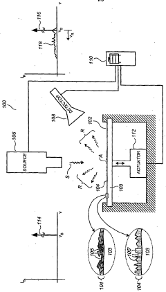
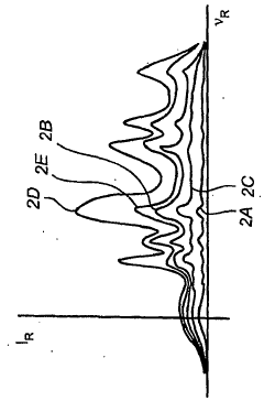
- A SERS system with a deformable SERS-active structure actuated by mechanical, electrostatic, or pneumatic means to control the intensity of Raman-scattered radiation, allowing for real-time tuning of hot-spot conditions by varying the deformation of the SERS-active structure near analyte molecules.
Surface enhanced raman scattering (SERS) apparatus, methods and applications
PatentActiveUS9001322B2
Innovation
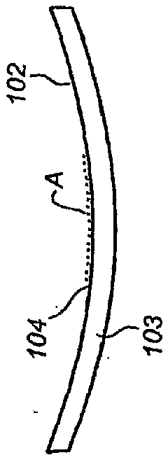
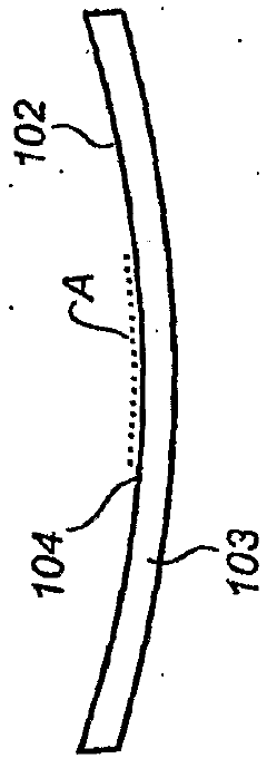
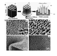
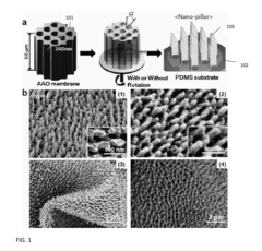
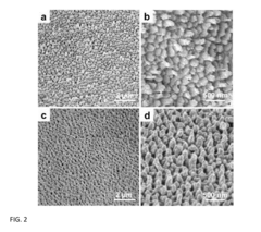
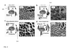
- The development of a shadow mask assisted evaporation (SMAE) method for fabricating SERS-enhanced nanostructured substrates with controlled nanostructures, including arrays of elongate shapes like nano-pillars, nano-nibs, and nano-triangular tips on flexible substrates, allowing for adjustable spacing and integration with functionalized nanoparticles for enhanced sensitivity.
Material Compatibility and Interface Engineering Considerations
The integration of SERS substrates with semiconductor devices presents significant material compatibility challenges that must be addressed through careful interface engineering. Noble metals commonly used in SERS substrates, such as gold, silver, and copper, can introduce contamination issues when in direct contact with semiconductor materials, particularly silicon. These metals can diffuse into the semiconductor lattice, creating deep-level traps that severely degrade device performance through increased leakage currents and reduced carrier lifetimes.
Adhesion between SERS substrates and semiconductor surfaces represents another critical consideration. Poor adhesion can lead to delamination during subsequent processing steps or device operation, compromising both SERS enhancement capabilities and device reliability. Various adhesion promotion techniques have been developed, including the use of titanium or chromium adhesion layers, surface functionalization with silanes, and plasma treatment protocols that modify surface energy without introducing contaminants.
Thermal compatibility issues arise from the significant coefficient of thermal expansion (CTE) mismatch between metallic SERS structures and semiconductor substrates. During thermal cycling in device fabrication or operation, this mismatch generates mechanical stress that can induce defects, cracking, or delamination. Advanced interface engineering approaches include the implementation of stress-buffering interlayers and gradient material structures that provide smoother transitions between dissimilar materials.
Chemical compatibility must be maintained throughout all processing steps. SERS substrate materials must withstand exposure to various chemicals used in semiconductor fabrication, including photoresist developers, etchants, and cleaning solutions. Conversely, the presence of SERS materials must not compromise the effectiveness of standard semiconductor processes or introduce cross-contamination in shared equipment.
Interface engineering strategies have evolved to address these challenges, with particular focus on barrier layers that prevent metal diffusion while maintaining SERS enhancement. Dielectric spacers such as SiO2, Al2O3, and Si3N4 have proven effective when precisely controlled at nanometer thicknesses. These spacers simultaneously prevent diffusion and can be engineered to optimize the electromagnetic field enhancement at the SERS-active surface.
Recent advances in atomic layer deposition (ALD) techniques have enabled precise control over interface properties, allowing for conformal coating of complex SERS nanostructures with ultrathin barrier layers. This approach preserves the high-aspect-ratio features necessary for SERS enhancement while providing effective isolation from the semiconductor device layers.
Manufacturing Scalability and Cost-Effectiveness Analysis
The scalability of SERS substrate manufacturing represents a critical factor in determining their viability for semiconductor industry integration. Current production methods for high-quality SERS substrates predominantly rely on sophisticated nanofabrication techniques such as electron-beam lithography and focused ion beam milling, which deliver excellent performance but at prohibitively high costs for large-scale semiconductor manufacturing. These precision-oriented approaches typically yield production rates of only 1-2 wafers per hour, creating a significant bottleneck for integration into high-volume semiconductor fabrication lines that process hundreds of wafers daily.
Cost analysis reveals that premium SERS substrates can range from $50-200 per square centimeter, primarily due to the specialized equipment requirements and low throughput. This represents a substantial cost barrier when semiconductor manufacturers aim to maintain overall production costs below $10 per square centimeter for competitive device pricing. The economic viability threshold for SERS integration likely requires a 5-10x reduction in substrate manufacturing costs to align with semiconductor industry economics.
Recent advancements in nanoimprint lithography and template-assisted self-assembly show promising directions for scalable manufacturing. These approaches have demonstrated the capability to produce SERS substrates with enhancement factors exceeding 10^6 at throughput rates approaching 15-20 wafers per hour. Additionally, roll-to-roll manufacturing techniques being developed by companies like Renishaw and Silmeco offer potential pathways to dramatically increase production volume while reducing per-unit costs by an estimated 60-75%.
Material selection also significantly impacts manufacturing economics. While gold and silver provide superior SERS enhancement, their high material costs limit scalability. Research into aluminum-based SERS substrates shows potential for reducing material costs by up to 80% while maintaining acceptable enhancement factors around 10^5, sufficient for many semiconductor monitoring applications.
Yield consistency remains a critical challenge, with current large-scale manufacturing methods showing 15-25% variation in SERS enhancement across a single wafer. This variability must be reduced to below 10% to meet semiconductor industry quality standards. Companies pioneering automated quality control systems using machine learning algorithms have demonstrated promising results in identifying and compensating for manufacturing inconsistencies, potentially improving yield rates by 30-40%.
The economic inflection point for widespread SERS adoption in semiconductor manufacturing appears to be approaching, with industry analysts projecting that manufacturing costs could reach competitive levels within 3-5 years as production technologies mature and economies of scale are realized.
Unlock deeper insights with PatSnap Eureka Quick Research — get a full tech report to explore trends and direct your research. Try now!
Generate Your Research Report Instantly with AI Agent
Supercharge your innovation with PatSnap Eureka AI Agent Platform!