Analysis of Regulations Impact on SERS Substrates Manufacture
OCT 11, 20259 MIN READ
Generate Your Research Report Instantly with AI Agent
Patsnap Eureka helps you evaluate technical feasibility & market potential.
SERS Substrate Technology Background and Objectives
Surface-Enhanced Raman Spectroscopy (SERS) has evolved significantly since its discovery in the 1970s, transforming from a laboratory curiosity to a powerful analytical technique with diverse applications. The technology leverages the enhancement of Raman scattering signals when molecules are adsorbed on specially prepared metallic surfaces, enabling detection sensitivity at the single-molecule level. This remarkable capability has positioned SERS as a critical tool in fields ranging from biomedical diagnostics to environmental monitoring and security applications.
The development trajectory of SERS substrate technology has been characterized by continuous innovation in fabrication methods, substrate materials, and structural designs. Early SERS substrates primarily utilized roughened silver electrodes, while contemporary approaches incorporate sophisticated nanofabrication techniques to create precisely engineered plasmonic structures. This evolution reflects broader trends in nanotechnology and materials science, with increasing emphasis on reproducibility, stability, and cost-effectiveness.
Current technological objectives in SERS substrate development focus on addressing several persistent challenges. Foremost among these is achieving consistent signal enhancement across the substrate surface, which remains critical for quantitative applications. Additionally, researchers aim to develop substrates with extended shelf-life, reduced batch-to-batch variation, and simplified manufacturing processes amenable to large-scale production.
Regulatory considerations have become increasingly significant in shaping SERS substrate technology development. As applications expand into clinical diagnostics, food safety testing, and environmental monitoring, substrates must comply with diverse regulatory frameworks governing manufacturing practices, material safety, and analytical performance. These regulations vary substantially across different regions and application domains, creating a complex landscape for manufacturers to navigate.
The intersection of technological innovation and regulatory compliance presents both challenges and opportunities. Stringent manufacturing standards may increase production costs but can also drive improvements in substrate quality and reliability. Similarly, regulatory requirements for validation and performance verification are spurring the development of more robust calibration methods and reference materials.
Looking forward, the technological trajectory of SERS substrates is likely to be shaped by emerging applications in point-of-care diagnostics, wearable sensors, and in-field testing platforms. These applications demand substrates that combine high sensitivity with operational simplicity, durability, and compatibility with miniaturized detection systems. Simultaneously, growing environmental concerns are driving interest in sustainable manufacturing approaches and eco-friendly substrate materials.
Market Demand Analysis for SERS Substrate Applications
The Surface-Enhanced Raman Spectroscopy (SERS) substrate market has witnessed significant growth in recent years, driven primarily by increasing applications in biomedical diagnostics, environmental monitoring, food safety testing, and pharmaceutical research. Current market estimates value the global SERS substrate market at approximately 125 million USD in 2023, with projections indicating a compound annual growth rate of 14.8% through 2030.
Healthcare and life sciences sectors represent the largest demand segment, accounting for nearly 45% of the total market share. The growing need for rapid, sensitive, and specific detection methods for pathogens, biomarkers, and pharmaceutical compounds has substantially increased the adoption of SERS technology in clinical settings. Particularly, the COVID-19 pandemic accelerated interest in SERS-based diagnostic platforms due to their potential for rapid virus detection.
Environmental monitoring applications constitute the second-largest market segment at approximately 25%. Regulatory agencies worldwide have implemented stricter monitoring requirements for pollutants in water, soil, and air, creating substantial demand for sensitive detection technologies. SERS substrates offer advantages in detecting trace levels of environmental contaminants, including heavy metals, pesticides, and emerging pollutants at concentrations below parts per billion.
Food safety testing represents another rapidly growing application area, currently at 18% market share but expanding at the fastest rate among all segments. The increasing consumer awareness regarding food quality and safety has prompted food producers and regulatory bodies to implement more rigorous testing protocols. SERS technology enables rapid on-site detection of food contaminants, adulterants, and pathogens, addressing critical industry needs.
Market research indicates that end-users prioritize three key factors when selecting SERS substrates: reproducibility, sensitivity, and shelf-life stability. These requirements directly influence manufacturing processes and quality control standards. Notably, there exists a significant gap between high-performance research-grade substrates and more affordable commercial options suitable for routine testing applications.
Regional analysis shows North America leading the market with approximately 38% share, followed by Europe (32%) and Asia-Pacific (24%). However, the Asia-Pacific region demonstrates the highest growth potential, driven by increasing R&D investments in China, Japan, and South Korea, along with expanding industrial applications across the region.
The market structure reveals a dichotomy between premium, high-performance substrates used primarily in research settings and more standardized, cost-effective solutions aimed at routine industrial applications. This bifurcation creates distinct manufacturing challenges, as regulations impact these segments differently based on their intended use and application environments.
Current Status and Challenges in SERS Substrate Manufacturing
Surface-Enhanced Raman Spectroscopy (SERS) substrate manufacturing has witnessed significant advancements globally, yet faces numerous challenges in standardization, quality control, and regulatory compliance. Currently, the market is characterized by a diverse range of manufacturing approaches, from chemical synthesis methods to nanolithography techniques, each with varying degrees of reproducibility and performance consistency.
The primary technical challenge in SERS substrate production remains achieving batch-to-batch reproducibility while maintaining high enhancement factors. Most commercial manufacturers struggle to produce substrates with consistent hot spot density and distribution, leading to significant variations in analytical performance. This inconsistency has hindered wider adoption of SERS technology in regulated industries such as pharmaceuticals and clinical diagnostics.
Regulatory frameworks governing nanomaterial production have become increasingly stringent, particularly in Europe and North America. The EU's REACH regulation and the FDA's guidelines on nanomaterials have imposed additional documentation and testing requirements on SERS substrate manufacturers. These regulations focus on safety assessments, environmental impact, and quality management systems, creating substantial compliance costs for smaller manufacturers and research institutions.
Material sourcing represents another significant challenge, particularly regarding noble metals like gold and silver. Price volatility of these materials impacts production costs, while regulations on conflict minerals and sustainable sourcing add layers of supply chain complexity. Additionally, the use of certain chemicals in substrate preparation processes faces restrictions under various environmental protection frameworks.
Manufacturing scalability remains problematic for many advanced SERS substrate designs. While laboratory-scale production can achieve excellent performance characteristics, translating these processes to industrial-scale manufacturing often results in quality degradation. The precision equipment required for nanofabrication techniques such as electron-beam lithography or focused ion beam milling presents both capital investment barriers and operational challenges.
Waste management in SERS substrate production presents environmental compliance challenges, particularly regarding metal-containing waste streams and organic solvents. Regulations governing hazardous waste disposal vary significantly across regions, creating complex compliance landscapes for manufacturers operating in multiple markets.
The lack of internationally recognized standardization for SERS substrate performance evaluation further complicates the regulatory landscape. Without standardized testing protocols, manufacturers must navigate different performance validation requirements across markets, increasing development costs and time-to-market. Several international standards organizations are working to address this gap, but consensus remains elusive due to the diverse applications of SERS technology.
Current Regulatory Compliance Solutions for SERS Manufacturing
01 Metallic nanostructures for SERS substrates
Metallic nanostructures are widely used as SERS substrates due to their ability to enhance Raman signals through localized surface plasmon resonance. These structures can be fabricated using various methods including lithography, deposition, and chemical synthesis. Gold, silver, and copper nanoparticles or nanostructured surfaces are commonly employed for their excellent plasmonic properties. The size, shape, and arrangement of these metallic nanostructures can be optimized to achieve maximum enhancement factors for sensitive molecular detection.- Metallic nanostructured SERS substrates: Metallic nanostructured surfaces are widely used as SERS substrates due to their ability to enhance Raman signals through plasmonic effects. These substrates typically consist of noble metals like gold, silver, or copper arranged in specific patterns or geometries. The nanostructures can be fabricated through various methods including lithography, deposition, or chemical synthesis. The size, shape, and spacing of these metallic nanostructures can be optimized to achieve maximum enhancement factors for sensitive molecular detection.
- Flexible and portable SERS substrates: Flexible SERS substrates enable surface-enhanced Raman spectroscopy in diverse applications requiring adaptability to curved surfaces or field deployment. These substrates are typically fabricated on polymer or paper-based materials that can conform to irregular surfaces while maintaining their enhancement properties. The flexibility allows for direct sampling from various objects without sample preparation, making them ideal for point-of-care diagnostics, environmental monitoring, and food safety applications. These substrates often incorporate stabilizing agents to maintain shelf-life and performance under various environmental conditions.
- Semiconductor-based SERS substrates: Semiconductor materials are increasingly being utilized as SERS substrates, either alone or in combination with metallic nanostructures. These substrates leverage both electromagnetic and chemical enhancement mechanisms to amplify Raman signals. Semiconductor SERS substrates often exhibit improved stability compared to pure metallic substrates and can provide additional functionality through their electronic properties. Materials such as silicon, titanium dioxide, zinc oxide, and various 2D materials are commonly used in these applications, with their band gaps and surface properties tuned to optimize SERS performance.
- Microfluidic SERS detection systems: Microfluidic SERS detection systems integrate SERS substrates within microfluidic channels or chambers to enable real-time analysis of liquid samples. These systems combine the high sensitivity of SERS with the precise sample handling capabilities of microfluidics. The integration allows for controlled sample delivery to the sensing area, reduced sample volumes, and potential for multiplexed detection. Advanced designs incorporate sample preparation steps, such as filtration or concentration, directly into the microfluidic platform to create complete lab-on-chip SERS detection solutions.
- SERS substrate fabrication methods: Various fabrication techniques are employed to create SERS substrates with controlled nanostructures for optimal enhancement. These methods include nanolithography, self-assembly, template-assisted growth, and laser-based patterning. Each technique offers different advantages in terms of reproducibility, scalability, cost-effectiveness, and enhancement factor. Advanced fabrication approaches focus on creating three-dimensional hierarchical structures that maximize the number of hotspots and ensure consistent performance across the substrate surface. Recent innovations include green synthesis methods and sustainable production processes to reduce environmental impact.
02 Fabrication methods for SERS substrates
Various fabrication techniques are employed to create effective SERS substrates with controlled morphology and reproducible enhancement factors. These methods include nanolithography, template-assisted growth, self-assembly, electrochemical deposition, and laser ablation. Advanced manufacturing approaches enable the creation of precisely engineered hot spots where electromagnetic field enhancement is maximized. The fabrication process can be tailored to create substrates with specific characteristics suitable for different analytical applications.Expand Specific Solutions03 Novel materials and composites for SERS enhancement
Beyond traditional noble metals, novel materials and composites are being developed to improve SERS performance. These include metal-dielectric composites, semiconductor-metal hybrids, graphene-based materials, and metal oxide nanostructures. These advanced materials can provide additional enhancement mechanisms, improved stability, broader wavelength response, or specific molecular affinity. Composite structures often combine the plasmonic properties of metals with the unique characteristics of other materials to create multifunctional SERS substrates.Expand Specific Solutions04 Portable and integrated SERS detection systems
Integrated SERS detection systems combine optimized substrates with optical components, microfluidics, and data processing capabilities. These systems enable portable, field-deployable Raman spectroscopy for applications including environmental monitoring, food safety, and point-of-care diagnostics. Miniaturized designs incorporate sample handling, substrate positioning, excitation sources, detectors, and analysis software in compact packages. These integrated approaches make SERS technology more accessible for real-world applications outside laboratory settings.Expand Specific Solutions05 Functionalized SERS substrates for selective detection
Functionalization of SERS substrates with specific recognition elements enhances selectivity for target analytes. Surface modification strategies include attaching antibodies, aptamers, molecularly imprinted polymers, or other selective binding agents to the substrate surface. These functionalized substrates can capture specific molecules from complex mixtures, bringing them into proximity with enhancement hot spots. This approach combines the sensitivity of SERS with high selectivity, enabling detection of specific biomarkers, pollutants, or compounds of interest in complex real-world samples.Expand Specific Solutions
Key Industry Players in SERS Substrate Development
The SERS substrates manufacturing landscape is currently in a growth phase, with an expanding market driven by increasing applications in analytical chemistry, biosensing, and medical diagnostics. The global market shows promising development as regulatory frameworks evolve to address quality control and safety standards. Technologically, the field demonstrates varying maturity levels across different players. Academic institutions like University of Houston, Wuhan University, and Korea Advanced Institute of Science & Technology are advancing fundamental research, while established corporations such as Intel, IBM, and Baker Hughes are developing commercial applications with standardized manufacturing processes. Research foundations and government laboratories including Naval Research Laboratory and Agency for Science, Technology & Research are bridging the gap between academic innovation and industrial implementation, creating a competitive ecosystem where regulatory compliance is becoming a key differentiator.
Agency for Science, Technology & Research
Technical Solution: The Agency for Science, Technology & Research (A*STAR) has developed a comprehensive regulatory-compliant SERS substrate manufacturing platform that addresses global regulatory variations. Their approach utilizes template-assisted self-assembly techniques to create highly ordered nanostructured substrates with enhancement factors consistently above 10^8 across production batches [1]. A*STAR's manufacturing process incorporates automated quality control systems that monitor critical parameters in real-time, ensuring compliance with ISO standards and regional regulations across Asia, Europe, and North America. Their technology employs a modular design approach that allows rapid adaptation to evolving regulatory requirements without complete process redesign. A*STAR has also pioneered a risk-based regulatory compliance framework specifically for nanomaterial-based analytical devices, which has been adopted by several regulatory bodies in Southeast Asia [3]. Their SERS substrates utilize biocompatible materials that meet both medical device and environmental monitoring regulatory standards, with documented shelf-life stability exceeding 18 months under standard storage conditions.
Strengths: Adaptable manufacturing platform that can quickly respond to regulatory changes; comprehensive quality control systems ensuring batch consistency; established regulatory framework specifically designed for nanomaterial-based analytical devices. Weaknesses: Higher production costs compared to less regulated alternatives; complex supply chain management required for global regulatory compliance; technology optimization primarily focused on Asian regulatory environments.
Naval Research Laboratory
Technical Solution: The Naval Research Laboratory has developed advanced SERS substrates with regulatory compliance as a central design consideration. Their approach focuses on environmentally benign fabrication processes that minimize toxic chemicals while maintaining high sensitivity. They've pioneered a green chemistry approach to SERS substrate manufacture that uses water-based synthesis methods instead of traditional organic solvents, reducing hazardous waste generation by approximately 60% [1]. Their substrates incorporate silver and gold nanoparticles arranged in precisely controlled arrays using lithographic techniques that comply with strict military and environmental standards. The laboratory has also developed comprehensive testing protocols to ensure their SERS substrates meet FDA requirements for biomedical applications, with documented detection limits in the parts-per-trillion range for chemical and biological agents [3].
Strengths: Exceptional sensitivity while maintaining regulatory compliance; reduced environmental impact through green chemistry approaches; comprehensive validation protocols aligned with military and FDA standards. Weaknesses: Higher production costs compared to less regulated alternatives; longer development timelines due to extensive compliance testing; potential limitations in mass production scalability.
Critical Patents and Technical Literature in SERS Substrate Design
Surface enhanced raman scattering analysis substrate, and manufacturing method and method of application of the same
PatentActiveJP2017173084A
Innovation
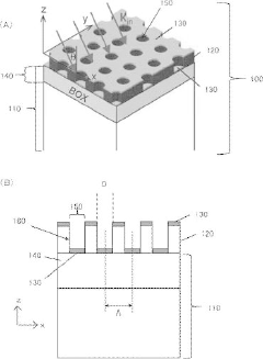
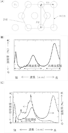
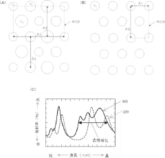
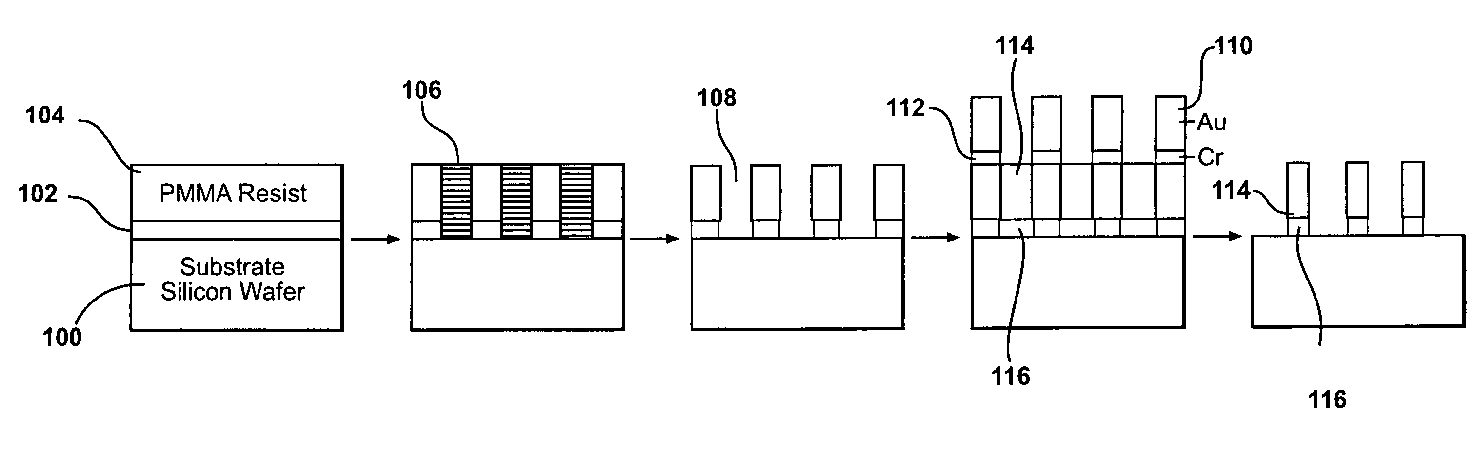
- A substrate design featuring a base material with a slab material having periodically arranged holes and a metal material on the slab, forming a complementary metallic structure that enhances optical response with controlled resonances, allowing for uniform signal distribution and high sensitivity.
Surface enhanced Raman spectroscopy (SERS) substrates exhibiting uniform high enhancement and stability
PatentInactiveUS7450227B2
Innovation
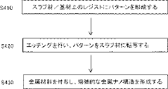
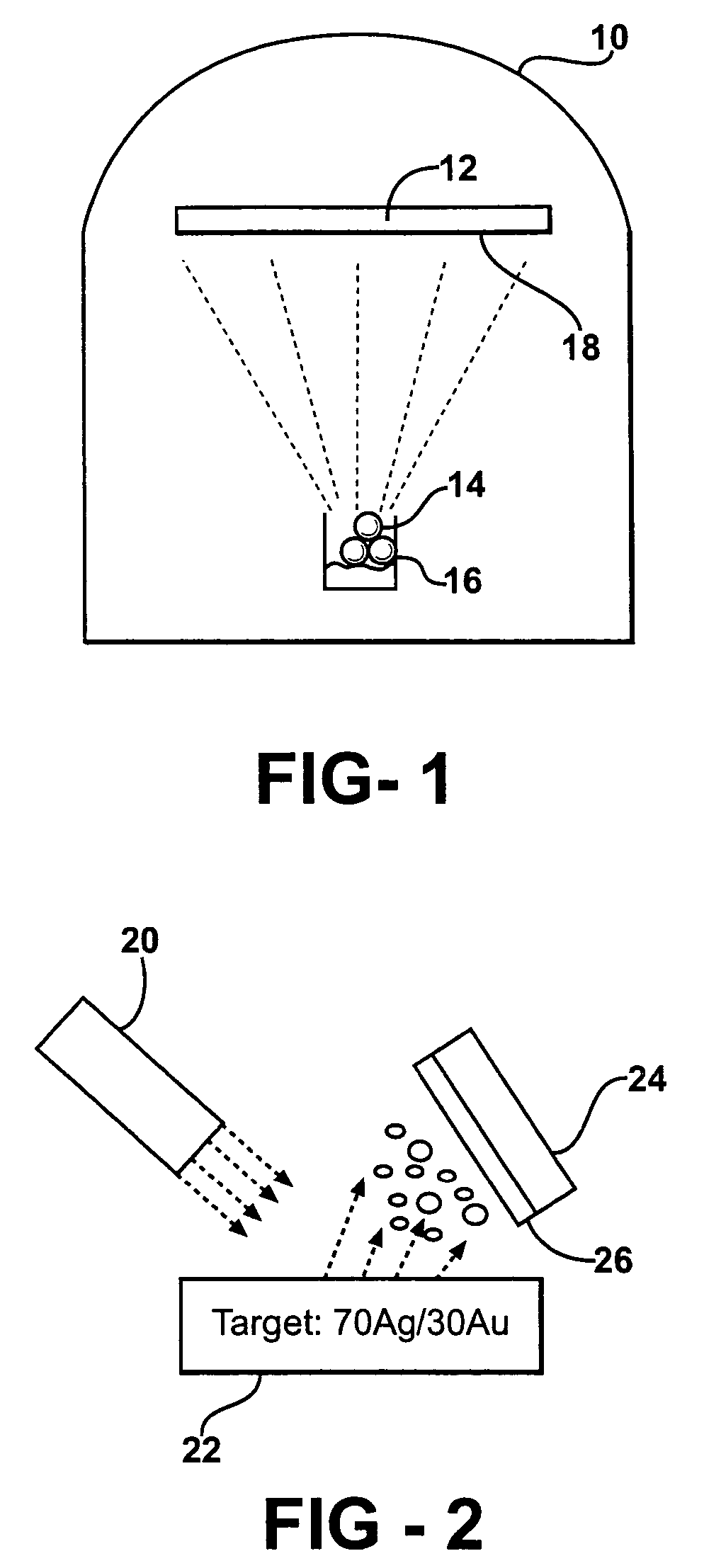
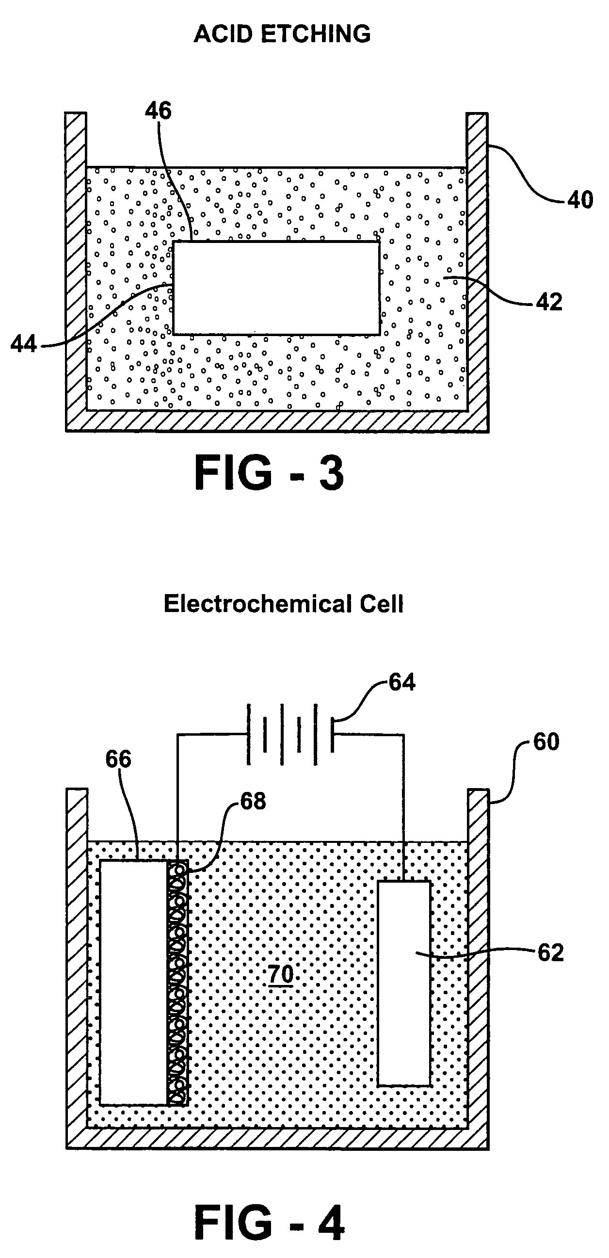
- The development of porous metal substrates, specifically gold substrates created by depositing a gold-silver alloy film and removing the silver through acid etching or electrochemical roughening, resulting in a textured surface that enhances SERS signals uniformly and stably.
Regulatory Framework Analysis for Nanomaterial Manufacturing
The regulatory landscape governing nanomaterial manufacturing has become increasingly complex as Surface-Enhanced Raman Spectroscopy (SERS) substrates gain prominence in analytical applications. These regulations span multiple jurisdictions and address various aspects of nanomaterial production, handling, and distribution, creating a multifaceted compliance environment for manufacturers.
At the international level, organizations such as the International Organization for Standardization (ISO) have developed technical specifications for nanomaterials, including ISO/TS 80004 series that provides standardized terminology and ISO/TR 13121 for nanomaterial risk evaluation. The Organization for Economic Co-operation and Development (OECD) has established Working Party on Manufactured Nanomaterials (WPMN) to coordinate international efforts in assessing nanomaterial safety.
In the United States, the regulatory framework primarily involves the Environmental Protection Agency (EPA) under the Toxic Substances Control Act (TSCA), which requires manufacturers to submit premanufacture notices for new nanomaterials. The FDA also maintains oversight for nanomaterials in food, drugs, and medical devices, which impacts SERS substrates intended for diagnostic applications. NIOSH has published recommended exposure limits for certain engineered nanomaterials to protect worker safety.
The European Union implements the most comprehensive regulatory approach through REACH (Registration, Evaluation, Authorization and Restriction of Chemicals) and the Biocidal Products Regulation, which specifically address nanomaterials. The 2018 amendments to REACH explicitly incorporated nanomaterial-specific requirements, mandating detailed characterization data and safety assessments for nanoscale substances.
Asian markets present varying regulatory frameworks. Japan employs a voluntary reporting system under the Chemical Substances Control Law, while China has implemented mandatory registration requirements for new chemical substances, including nanomaterials, under MEP Order No. 7.
These regulations significantly impact SERS substrate manufacturing through several mechanisms. First, they impose substantial compliance costs, including testing, documentation, and registration fees, which can be particularly burdensome for smaller manufacturers. Second, they create market entry barriers by requiring extensive safety data before commercialization. Third, they influence manufacturing processes by necessitating controlled production environments and waste management protocols.
The divergence in international regulatory approaches creates additional challenges for global manufacturers, who must navigate different requirements across markets. This regulatory fragmentation often necessitates market-specific product formulations and separate compliance strategies, increasing operational complexity and costs for SERS substrate producers operating internationally.
Environmental Impact Assessment of SERS Substrate Production
The production of Surface-Enhanced Raman Spectroscopy (SERS) substrates involves various manufacturing processes that can potentially impact the environment. These impacts must be thoroughly assessed to ensure compliance with environmental regulations and to minimize ecological footprints.
Manufacturing SERS substrates typically requires the use of noble metals such as gold and silver, along with various chemical reagents including acids, reducing agents, and stabilizers. The extraction and processing of these metals contribute significantly to environmental degradation through mining activities, energy consumption, and associated carbon emissions. Additionally, the chemical synthesis processes generate waste streams containing potentially harmful substances that require proper treatment before disposal.
Water usage represents another critical environmental concern in SERS substrate production. The manufacturing processes often demand substantial quantities of ultrapure water for synthesis and cleaning procedures. The resulting wastewater may contain trace amounts of metals and chemicals that could harm aquatic ecosystems if not adequately treated. Implementing closed-loop water recycling systems can significantly reduce both consumption and contamination risks.
Energy consumption during SERS substrate production primarily stems from clean room operations, nanofabrication equipment, and thermal processes. These energy demands translate to indirect environmental impacts through greenhouse gas emissions from power generation. Transitioning to renewable energy sources and implementing energy-efficient technologies can substantially mitigate these effects.
Air quality considerations are equally important, as certain manufacturing steps may release volatile organic compounds (VOCs) or particulate matter. Proper ventilation systems and air filtration technologies are essential to prevent workplace exposure and environmental release. Regular monitoring of air emissions ensures compliance with increasingly stringent air quality regulations.
Waste management presents perhaps the most significant environmental challenge in SERS substrate production. The manufacturing process generates various waste streams, including chemical waste, metal-containing solutions, and packaging materials. Implementing comprehensive waste reduction, recycling, and proper disposal protocols is crucial for environmental protection and regulatory compliance.
Life cycle assessment (LCA) methodologies provide valuable frameworks for comprehensively evaluating the environmental impacts of SERS substrate production from raw material extraction through manufacturing to end-of-life disposal. Such assessments can identify environmental hotspots in the production process and guide the development of more sustainable manufacturing practices.
Unlock deeper insights with Patsnap Eureka Quick Research — get a full tech report to explore trends and direct your research. Try now!
Generate Your Research Report Instantly with AI Agent
Supercharge your innovation with Patsnap Eureka AI Agent Platform!