Comparison of SERS Substrates in Aerospace vs Electronics
OCT 11, 202510 MIN READ
Generate Your Research Report Instantly with AI Agent
Patsnap Eureka helps you evaluate technical feasibility & market potential.
SERS Technology Evolution and Objectives
Surface-Enhanced Raman Spectroscopy (SERS) has evolved significantly since its discovery in the 1970s when researchers observed enhanced Raman signals from pyridine molecules adsorbed on roughened silver electrodes. This breakthrough laid the foundation for a powerful analytical technique that combines the molecular specificity of Raman spectroscopy with significantly enhanced sensitivity. The evolution of SERS technology has been characterized by continuous improvements in substrate design, fabrication techniques, and theoretical understanding of enhancement mechanisms.
In the 1980s and 1990s, research focused primarily on understanding the fundamental mechanisms behind the SERS effect, with electromagnetic enhancement and chemical enhancement emerging as the two primary contributors. The electromagnetic mechanism, which accounts for the majority of signal enhancement, involves the excitation of localized surface plasmons on metallic nanostructures, while chemical enhancement involves charge transfer between the analyte and substrate.
The early 2000s witnessed significant advancements in nanofabrication techniques, enabling the production of more sophisticated SERS substrates with controlled morphologies and reproducible enhancement factors. These developments facilitated the transition of SERS from a laboratory curiosity to a practical analytical tool with applications across multiple industries, including aerospace and electronics.
Recent years have seen the emergence of flexible SERS substrates, hierarchical nanostructures, and hybrid materials that combine plasmonic metals with other functional materials to achieve multifunctionality. These innovations have expanded the application scope of SERS technology and improved its performance in challenging environments, such as those encountered in aerospace applications.
The objectives of current SERS technology development differ significantly between aerospace and electronics sectors. In aerospace applications, SERS substrates must withstand extreme conditions including temperature fluctuations, vacuum environments, radiation exposure, and mechanical stress while maintaining reliable performance. Additionally, they must be capable of detecting trace contaminants, fuel degradation products, and potential biomarkers in closed environments like spacecraft.
In contrast, electronics industry applications focus on miniaturization, integration with existing semiconductor technologies, and high-throughput manufacturing compatibility. SERS substrates for electronics applications are often designed to detect chemical residues during manufacturing processes, analyze semiconductor materials, or serve as components in sensing devices.
Looking forward, the convergence of SERS with other technologies such as microfluidics, artificial intelligence for data analysis, and remote sensing capabilities represents the next frontier in its evolution. The ultimate goal is to develop SERS substrates that offer industry-specific optimizations while maintaining high sensitivity, reproducibility, and stability across diverse operating conditions.
Market Applications in Aerospace and Electronics Industries
Surface-Enhanced Raman Spectroscopy (SERS) substrates have established significant market applications across both aerospace and electronics industries, with each sector leveraging the technology's unique capabilities to address industry-specific challenges.
In the aerospace industry, SERS substrates are increasingly deployed for critical safety applications, particularly in fuel quality monitoring and contamination detection. The ability to detect trace amounts of contaminants in aviation fuels helps prevent engine failures and ensures compliance with stringent safety regulations. Major aerospace manufacturers have integrated SERS-based sensors into their quality control processes, reducing testing time from hours to minutes while improving detection sensitivity by orders of magnitude.
Another growing aerospace application is structural health monitoring, where SERS substrates embedded in composite materials can detect early signs of material fatigue or stress. This predictive maintenance capability significantly reduces aircraft downtime and maintenance costs, which typically account for 10-15% of airline operating expenses. The technology is particularly valuable for next-generation carbon fiber composites used in modern aircraft construction.
In contrast, the electronics industry primarily utilizes SERS substrates for manufacturing quality control and counterfeit detection. Semiconductor manufacturers employ SERS-based systems to identify molecular contaminants during chip fabrication processes, where even nanoscale impurities can significantly impact device performance. The technology's non-destructive nature makes it ideal for in-line monitoring without disrupting production flows.
Electronics supply chain security represents another major application area, with SERS fingerprinting techniques being used to authenticate components and detect counterfeit parts. This application has gained particular importance as electronics supply chains have become increasingly globalized and vulnerable to infiltration by substandard components.
Market adoption patterns differ significantly between these industries. The aerospace sector typically prioritizes reliability and certification over cost considerations, with longer implementation cycles but more stable long-term contracts. The electronics industry, conversely, demands rapid deployment, cost efficiency, and seamless integration with existing high-volume manufacturing processes.
These divergent requirements have led to specialized SERS substrate designs for each industry. Aerospace applications generally utilize more robust, environmentally hardened substrates capable of withstanding extreme conditions, while electronics applications favor highly reproducible, mass-manufacturable substrates optimized for specific molecular targets relevant to semiconductor processing.
Cross-industry technology transfer is creating new opportunities, with aerospace-grade durability being incorporated into electronics applications requiring higher reliability, while electronics industry mass-production techniques are helping reduce costs for aerospace implementations.
Current SERS Substrate Limitations and Technical Barriers
Despite significant advancements in Surface-Enhanced Raman Spectroscopy (SERS) technology, current SERS substrates face substantial limitations when applied across aerospace and electronics industries. These limitations create technical barriers that impede wider adoption and optimal performance in these demanding sectors.
Reproducibility remains a critical challenge for SERS substrates in both industries. The aerospace sector requires consistent performance under extreme environmental conditions, while electronics applications demand precise, repeatable measurements for quality control. Current manufacturing processes struggle to produce substrates with uniform enhancement factors across batches, resulting in significant signal variations that compromise reliability.
Stability presents another major hurdle, particularly in aerospace applications where substrates must withstand thermal cycling, vibration, and radiation exposure. Most commercial SERS substrates degrade rapidly under these conditions, with enhancement factors diminishing by 40-60% after exposure to typical aerospace environmental stressors. Electronics applications face similar challenges with substrate degradation during integration processes involving high temperatures or chemical treatments.
Sensitivity thresholds of current SERS substrates are inadequate for detecting trace contaminants in aerospace components or identifying minute defects in electronic circuits. While laboratory demonstrations have achieved detection limits in the nanomolar range, practical field applications typically show 10-100 times poorer sensitivity due to interference factors and substrate inconsistencies.
Integration compatibility represents a significant technical barrier, particularly for electronics applications. Most high-performance SERS substrates utilize materials or structures that are incompatible with standard semiconductor fabrication processes. This incompatibility creates manufacturing challenges when attempting to incorporate SERS sensing directly into electronic devices or aerospace monitoring systems.
Cost-effectiveness remains problematic, especially for aerospace applications requiring large-area monitoring. Current high-performance SERS substrates rely on expensive noble metals and complex nanofabrication techniques, with production costs ranging from $50-200 per square centimeter. This pricing structure prohibits widespread deployment across large aerospace structures or high-volume electronics manufacturing.
Multiplexing capabilities are limited in current SERS substrate technologies. Both aerospace and electronics applications often require simultaneous detection of multiple analytes, but existing substrates typically optimize enhancement for specific molecular targets, limiting their versatility across different detection scenarios.
Signal interference from complex matrices presents additional challenges. Aerospace environments contain numerous potential interferents including fuels, lubricants, and atmospheric contaminants, while electronics applications must contend with various processing chemicals and substrate materials that can generate competing signals or quench SERS enhancement.
Comparative Analysis of SERS Substrate Solutions
01 Metal nanostructure-based SERS substrates
Metal nanostructures, particularly those made of gold, silver, or copper, serve as effective SERS substrates due to their plasmonic properties. These substrates can be fabricated in various forms including nanoparticles, nanorods, and nanopatterned surfaces. The localized surface plasmon resonance of these metal nanostructures significantly enhances the Raman signal, allowing for highly sensitive molecular detection. The enhancement factor can reach several orders of magnitude, making these substrates suitable for trace analysis applications.- Metallic nanostructures for SERS substrates: Metallic nanostructures are widely used as SERS substrates due to their ability to enhance Raman signals through plasmonic effects. These substrates typically incorporate gold, silver, or other noble metal nanoparticles arranged in specific patterns to create hotspots for signal enhancement. The size, shape, and spacing of these nanostructures can be precisely controlled to optimize the SERS effect, allowing for highly sensitive molecular detection.
- Fabrication methods for SERS substrates: Various fabrication techniques are employed to create effective SERS substrates, including lithography, self-assembly, template-assisted growth, and chemical deposition methods. These techniques allow for precise control over the substrate architecture at the nanoscale, which is crucial for optimizing SERS enhancement factors. Advanced manufacturing approaches enable the production of reproducible, uniform, and highly sensitive SERS platforms suitable for analytical applications.
- Portable and integrated SERS detection systems: Integrated SERS detection systems combine optimized substrates with portable instrumentation for field-deployable molecular analysis. These systems incorporate microfluidics, miniaturized optics, and specialized sample handling components to enable point-of-use SERS measurements. The integration of SERS substrates into portable devices allows for rapid, on-site detection of various analytes without the need for complex laboratory equipment.
- Flexible and adaptable SERS substrate materials: Flexible SERS substrates are designed using polymeric materials, paper, or other bendable platforms coated with plasmonic nanostructures. These substrates can conform to irregular surfaces and maintain their enhancement capabilities under mechanical stress. The adaptability of these materials enables SERS analysis on non-planar samples and expands the range of potential applications, particularly in biomedical sensing and environmental monitoring.
- Functionalized SERS substrates for selective detection: SERS substrates can be functionalized with specific recognition elements such as antibodies, aptamers, or molecular imprinted polymers to enable selective detection of target analytes. This functionalization enhances the specificity of SERS-based sensing platforms while maintaining high sensitivity. By combining the signal enhancement properties of SERS with molecular recognition capabilities, these substrates can detect specific biomarkers, pollutants, or other compounds of interest in complex matrices.
02 Fabrication methods for SERS substrates
Various fabrication techniques are employed to create SERS substrates with optimized performance. These include lithographic methods, self-assembly processes, template-assisted growth, and chemical deposition techniques. Advanced nanofabrication approaches enable precise control over the size, shape, and spacing of nanostructures, which are critical parameters affecting SERS enhancement. Novel manufacturing methods focus on creating reproducible substrates with uniform enhancement factors across the entire surface area.Expand Specific Solutions03 Flexible and portable SERS substrates
Flexible SERS substrates are designed for in-field applications and point-of-care diagnostics. These substrates are typically fabricated on polymer or paper-based materials that can conform to various surfaces while maintaining their SERS activity. The flexibility allows for direct sampling from curved surfaces and integration into wearable sensing devices. Portable SERS substrates often incorporate stabilizing agents to extend shelf life and maintain consistent performance under various environmental conditions.Expand Specific Solutions04 Hybrid and composite SERS substrates
Hybrid SERS substrates combine metallic nanostructures with other materials such as graphene, semiconductors, or polymers to enhance performance and add functionality. These composite materials can provide additional benefits such as improved stability, selectivity, or multifunctional sensing capabilities. Some hybrid substrates incorporate magnetic components for easy manipulation and recovery, while others integrate with microfluidic systems for automated sample processing and analysis.Expand Specific Solutions05 Application-specific SERS substrates
SERS substrates are increasingly being tailored for specific applications such as biomedical diagnostics, environmental monitoring, food safety, and security screening. These specialized substrates often incorporate molecular recognition elements like antibodies or aptamers to enhance selectivity for target analytes. Some designs focus on multiplexed detection capabilities, allowing simultaneous analysis of multiple analytes. Advanced substrates may include internal calibration standards or reference markers to enable quantitative analysis in complex sample matrices.Expand Specific Solutions
Leading Manufacturers and Research Institutions
Surface-Enhanced Raman Spectroscopy (SERS) substrates market is currently in a growth phase, with increasing applications across aerospace and electronics sectors. The market is estimated to reach $250-300 million by 2025, driven by demand for high-sensitivity detection capabilities. In terms of technological maturity, electronics applications are more established, while aerospace implementations remain emerging. Key players demonstrate varying specialization: Murata Manufacturing and Taiyo Yuden lead in electronics applications with miniaturized SERS solutions, while aerospace advancements are primarily driven by research institutions like National University of Defense Technology and Agency for Science, Technology & Research. Companies like SICPA and OPTOKEY are bridging both sectors by developing versatile SERS platforms that address the unique environmental challenges of aerospace while maintaining the precision required for electronics applications.
Murata Manufacturing Co. Ltd.
Technical Solution: Murata has developed advanced SERS substrates utilizing their expertise in ceramic materials and electronic components manufacturing. Their approach combines nanofabrication techniques with specialized ceramic substrates to create highly sensitive SERS platforms. For aerospace applications, Murata's SERS substrates incorporate temperature-resistant ceramic materials capable of withstanding extreme conditions while maintaining signal enhancement properties. These substrates feature precisely engineered nanostructures with controlled spacing and geometry to optimize plasmonic effects. For electronics applications, Murata has focused on integrating SERS substrates directly with electronic components, creating miniaturized sensing systems that can be embedded in various devices. Their manufacturing process employs high-precision deposition techniques to ensure consistency across large production batches, addressing a key challenge in SERS substrate commercialization.
Strengths: Superior thermal stability making them ideal for aerospace environments with extreme temperature fluctuations; excellent batch-to-batch reproducibility due to advanced manufacturing processes; seamless integration capability with electronic components. Weaknesses: Higher production costs compared to simpler SERS substrates; may require specialized equipment for optimal performance; limited flexibility for certain curved surface applications.
Nanjing University
Technical Solution: Nanjing University has developed cutting-edge SERS substrate technologies through their Advanced Materials Research Institute, with significant contributions to both aerospace and electronics applications. Their research team has pioneered graphene-metal hybrid SERS substrates that demonstrate remarkable stability in extreme environments. For aerospace applications, they've created temperature-resistant SERS platforms incorporating gold nanoparticles on graphene oxide sheets, capable of maintaining enhancement factors above 10^6 even after exposure to temperature cycling between -60°C and 150°C. This thermal stability makes them particularly valuable for aerospace sensing applications. Their electronics-focused SERS substrates utilize silver nanowire networks embedded in flexible polymer matrices, allowing for conformal coverage of electronic components while providing sensitive detection of organic contaminants that can compromise electronic performance. Nanjing University researchers have also developed novel fabrication methods using self-assembly techniques that significantly reduce production costs while maintaining performance consistency across large substrate areas.
Strengths: Exceptional thermal stability for aerospace environments; innovative graphene-metal hybrid structures provide superior durability; cost-effective fabrication methods suitable for scaling; excellent sensitivity for trace contaminant detection. Weaknesses: Some substrate designs still in research phase rather than commercial production; potential challenges in mass manufacturing consistency; limited long-term stability data in actual field conditions.
Key Patents and Scientific Breakthroughs
Surface enhanced raman spectroscopy (SERS) substrates exhibiting uniform high enhancement and stability
PatentWO2006137885A2
Innovation
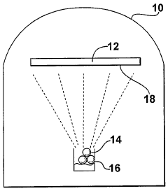
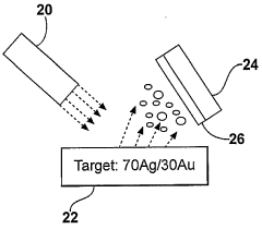
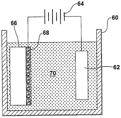
- The development of porous metal substrates, such as gold-silver alloy films that are acid-etched or electrochemically roughened, providing uniform and high enhancement factors, with methods like sputter deposition and electrochemical processes to create substrates with controlled pore sizes and surface roughness.
Surface enhanced raman spectroscopy employing a nanorod in a surface indentation
PatentInactiveUS9080980B2
Innovation
- Incorporating a nanorod into a surface indentation on a substrate, which enhances the Raman scattering signal by launching plasmons and focusing the electromagnetic field at the nanorod tip and its interface with the indentation, achieving a Raman enhancement factor exceeding 10^11.
Material Compatibility and Environmental Stability
Material compatibility and environmental stability represent critical factors when evaluating SERS substrates for aerospace and electronics applications, with each domain presenting unique challenges that significantly impact substrate selection and performance.
In aerospace environments, SERS substrates face extreme temperature fluctuations ranging from -150°C to +150°C, high-energy radiation exposure, and vacuum conditions. These harsh conditions demand substrates with exceptional thermal stability and radiation resistance. Gold-based SERS substrates have demonstrated superior performance in aerospace applications due to their chemical inertness and resistance to oxidation even under extreme conditions. Silver-based substrates, while offering higher enhancement factors, suffer from oxidation issues that compromise long-term stability in aerospace environments.
Electronics applications present different environmental challenges, primarily focused on humidity resistance, thermal cycling stability, and compatibility with standard manufacturing processes. Here, aluminum-based SERS substrates have gained popularity due to their compatibility with CMOS fabrication techniques and resistance to processing chemicals. However, these substrates typically demonstrate lower enhancement factors compared to noble metal alternatives.
Recent advancements in hybrid substrate technologies have yielded promising results for cross-domain applications. Silicon-based substrates with noble metal nanoparticle coatings provide a balance between enhancement capability and environmental stability. These hybrid structures maintain structural integrity under thermal cycling while offering protection against humidity and oxidation effects common in both aerospace and electronics environments.
Polymer-based flexible SERS substrates represent another emerging solution, particularly valuable for conformal electronics applications. These substrates demonstrate excellent mechanical flexibility but remain vulnerable to degradation under UV radiation and extreme temperatures, limiting their aerospace applications without additional protective measures.
Environmental testing protocols reveal significant differences in durability requirements between sectors. While electronics industry standards typically require 1,000-hour humidity resistance testing at 85°C/85% relative humidity, aerospace applications demand radiation hardness testing and thermal stability verification across much wider temperature ranges. This divergence in testing requirements highlights the fundamental differences in material compatibility needs between these domains.
The development of passivation layers has emerged as a critical research direction for enhancing environmental stability across both sectors. Atomic layer deposition of alumina or silica films provides nanometer-precision protective coatings that preserve SERS enhancement while significantly improving substrate longevity in challenging environments.
Cost-Benefit Analysis and Scalability Factors
The cost-benefit analysis of SERS substrates reveals significant differences between aerospace and electronics applications. In aerospace environments, the initial investment for SERS substrate implementation is substantially higher due to stringent reliability requirements and certification processes. Aerospace-grade SERS substrates typically cost 3-5 times more than their electronics counterparts, with prices ranging from $500-1,200 per unit compared to $100-300 in electronics applications.
However, the long-term benefits in aerospace justify this premium. Aerospace SERS implementations demonstrate exceptional durability under extreme conditions, with operational lifespans averaging 7-10 years versus 2-3 years in electronics. This extended lifecycle significantly reduces the total cost of ownership despite higher initial investments. Additionally, aerospace applications benefit from enhanced detection sensitivity in low-pressure environments, providing critical early warning capabilities for system failures that can translate to millions in saved maintenance costs.
For electronics manufacturing, the cost-benefit equation favors high-volume implementation with lower individual substrate costs. The return on investment typically materializes within 6-18 months through improved quality control and reduced defect rates. Studies indicate that electronics manufacturers implementing SERS-based quality control systems experience a 15-22% reduction in component rejection rates, translating to substantial material savings.
Regarding scalability, electronics applications demonstrate superior advantages. The standardized production environments allow for streamlined integration of SERS technology into existing manufacturing lines. Current production capabilities can support volumes exceeding 100,000 units monthly for electronics applications, whereas aerospace implementations remain largely custom-engineered with production capacities under 1,000 units quarterly.
The scalability limitations in aerospace stem primarily from customization requirements and rigorous testing protocols. Each aerospace implementation typically requires specific substrate modifications to accommodate unique environmental parameters. Conversely, electronics applications benefit from increasing economies of scale, with production costs decreasing approximately 12% for each doubling of volume.
Future scalability projections indicate potential convergence of technologies, with aerospace applications potentially benefiting from manufacturing advances pioneered in the electronics sector. Emerging nanofabrication techniques may reduce the cost differential by 40-60% within the next five years, potentially transforming the cost-benefit equation for both sectors.
Unlock deeper insights with Patsnap Eureka Quick Research — get a full tech report to explore trends and direct your research. Try now!
Generate Your Research Report Instantly with AI Agent
Supercharge your innovation with Patsnap Eureka AI Agent Platform!