Research on SERS Substrates in Semiconductor Coatings
OCT 11, 20259 MIN READ
Generate Your Research Report Instantly with AI Agent
Patsnap Eureka helps you evaluate technical feasibility & market potential.
SERS Substrate Evolution and Research Objectives
Surface-Enhanced Raman Spectroscopy (SERS) has evolved significantly since its discovery in the 1970s, transforming from an interesting optical phenomenon to a powerful analytical technique with applications spanning multiple industries. The evolution of SERS substrates represents a critical technological advancement that has enabled unprecedented molecular detection sensitivity, with enhancement factors reaching 10^10-10^11 compared to conventional Raman spectroscopy. This remarkable sensitivity allows for detection at the single-molecule level, opening new frontiers in analytical chemistry, biosensing, and materials science.
In the semiconductor coating industry, SERS substrates have gained particular attention due to their potential for non-destructive quality control, contaminant detection, and process monitoring. The integration of SERS-active materials with semiconductor manufacturing processes presents unique challenges and opportunities that drive current research efforts. Historical development shows a progression from simple roughened metal surfaces to precisely engineered nanostructures with optimized plasmonic properties.
The fundamental mechanism behind SERS involves electromagnetic field enhancement near metal nanostructures and chemical enhancement through charge transfer between analytes and substrate. Recent advances in nanofabrication techniques have enabled the creation of increasingly sophisticated SERS substrates with tailored properties for specific applications. These include periodic arrays of metal nanoparticles, nanogap structures, core-shell architectures, and hybrid materials combining plasmonic metals with semiconductor components.
Current technological trends indicate a growing interest in flexible, reusable, and environmentally stable SERS substrates that maintain consistent enhancement factors across large surface areas. Additionally, there is significant momentum toward developing SERS substrates that can be integrated directly into semiconductor manufacturing processes without introducing contamination or disrupting established workflows.
The primary research objectives in this field include developing SERS substrates with enhanced sensitivity and selectivity specifically for semiconductor coating applications. This involves optimizing substrate materials and geometries to detect trace contaminants and structural defects in semiconductor coatings at concentrations below parts-per-billion levels. Another critical goal is creating standardized fabrication methods that ensure reproducibility and scalability for industrial implementation.
Furthermore, researchers aim to develop in-line monitoring capabilities using SERS technology that can provide real-time feedback during semiconductor coating processes. This would enable immediate quality control and process optimization, significantly reducing waste and improving yield. The ultimate objective is to establish SERS as an indispensable analytical tool in semiconductor manufacturing, capable of addressing increasingly stringent quality requirements as device dimensions continue to shrink and performance demands escalate.
Market Applications of SERS in Semiconductor Industry
Surface-Enhanced Raman Spectroscopy (SERS) technology has found significant applications in the semiconductor industry, revolutionizing quality control, process monitoring, and material characterization. The semiconductor market's demand for SERS-based solutions has grown substantially due to increasing requirements for nanoscale analysis and non-destructive testing methods.
In semiconductor manufacturing, SERS substrates are primarily utilized for contaminant detection at extremely low concentrations. As semiconductor devices continue to shrink in size, even trace contaminants can significantly impact performance and yield. SERS technology enables manufacturers to detect organic and inorganic contaminants at parts-per-billion levels, which is crucial for maintaining high production standards in advanced node technologies.
Process monitoring represents another vital application area. SERS substrates integrated into semiconductor production lines provide real-time feedback on chemical reactions, etching processes, and deposition quality. This capability allows for immediate adjustments to manufacturing parameters, reducing waste and improving overall efficiency. Several leading semiconductor fabrication facilities have reported yield improvements of 5-7% after implementing SERS-based monitoring systems.
The characterization of thin films and coatings has emerged as a particularly valuable application. SERS substrates can analyze the molecular structure, thickness uniformity, and chemical composition of semiconductor coatings without damaging the sample. This non-destructive testing capability is especially important for evaluating high-value components and experimental materials during research and development phases.
Quality assurance departments increasingly rely on SERS technology for failure analysis. When semiconductor devices fail to meet performance specifications, SERS can identify molecular-level defects or contamination that might be undetectable through conventional analytical methods. This application has proven particularly valuable in identifying the root causes of systematic failures in new product lines.
The market for SERS applications in semiconductors is projected to grow significantly as the industry continues its push toward more advanced nodes and novel materials. Particularly promising is the integration of SERS with in-line monitoring systems and the development of specialized SERS substrates optimized for specific semiconductor materials and processes.
Emerging applications include the characterization of 2D materials like graphene and transition metal dichalcogenides, which are increasingly important in next-generation semiconductor devices. SERS substrates specifically designed for these novel materials are being developed to address the unique challenges they present in manufacturing and quality control.
Current SERS Substrate Technologies and Limitations
Surface-Enhanced Raman Spectroscopy (SERS) substrates have evolved significantly over the past decades, with current technologies broadly categorized into three main types: metal nanoparticle-based, nanopatterned, and hybrid substrates. Metal nanoparticle-based substrates, typically utilizing gold or silver nanoparticles, remain the most widely implemented due to their relatively straightforward fabrication and high enhancement factors. These substrates can achieve enhancement factors of 10^6 to 10^8, enabling detection limits at the single-molecule level under optimal conditions.
Nanopatterned substrates, including nanopillar arrays, nanoholes, and nanogratings, offer more consistent and reproducible SERS signals compared to nanoparticle-based alternatives. Advanced fabrication techniques such as electron-beam lithography and nanoimprint lithography have enabled precise control over the geometry and spacing of these nanostructures, which is crucial for optimizing the plasmonic properties that drive SERS enhancement.
Hybrid substrates, combining metallic nanostructures with semiconductor materials or other functional components, represent the cutting edge of SERS technology. These substrates can integrate multiple functionalities, such as photocatalytic activity or selective molecular binding, alongside SERS enhancement capabilities. Particularly relevant to semiconductor coatings are metal-semiconductor composites that leverage charge transfer mechanisms to further enhance Raman signals.
Despite these advancements, current SERS substrate technologies face several critical limitations. Reproducibility remains a significant challenge, with batch-to-batch variations often exceeding 20% in enhancement factors. This inconsistency severely hampers quantitative analysis applications, especially in quality control environments for semiconductor manufacturing.
Stability issues also plague many SERS substrates, with performance degradation occurring through oxidation, contamination, or structural changes over time. For semiconductor coating applications, where long-term monitoring may be required, this instability presents a major obstacle to practical implementation.
Uniformity across substrate surfaces represents another key limitation, with "hot spots" of extremely high enhancement often distributed non-uniformly. This spatial variability complicates mapping applications and reduces reliability in detecting trace contaminants in semiconductor coatings.
Integration challenges with existing semiconductor processing workflows further limit adoption. Many high-performance SERS substrates require fabrication conditions incompatible with standard semiconductor manufacturing processes, creating significant barriers to implementation.
Cost considerations also restrict widespread application, particularly for nanopatterned substrates requiring sophisticated fabrication techniques. While nanoparticle-based substrates offer more economical alternatives, they typically sacrifice reproducibility and uniformity—qualities essential for semiconductor quality control applications.
Mainstream SERS Substrate Fabrication Methods
01 Metallic nanostructures for SERS substrates
Metallic nanostructures are widely used as SERS substrates due to their ability to enhance Raman signals through plasmonic effects. These substrates typically incorporate gold, silver, or other noble metal nanoparticles arranged in specific patterns or geometries to create hotspots for signal enhancement. The size, shape, and spacing of these nanostructures can be engineered to optimize the SERS effect for different applications, including molecular detection and analysis.- Metallic nanostructures for SERS substrates: Metallic nanostructures are widely used as SERS substrates due to their plasmonic properties that enhance Raman signals. These structures can be fabricated using various methods including lithography, deposition, and chemical synthesis. Gold, silver, and copper nanoparticles or nanostructured surfaces are commonly employed for their strong localized surface plasmon resonance effects, which create 'hot spots' that significantly amplify the Raman signal of analyte molecules. The size, shape, and spacing of these metallic nanostructures can be optimized to achieve maximum enhancement factors.
- Flexible and portable SERS substrate designs: Flexible and portable SERS substrates enable on-site detection and analysis in various environments. These substrates are typically fabricated on bendable materials such as polymers or paper, allowing them to conform to irregular surfaces while maintaining their enhancement capabilities. Portable designs often incorporate features that facilitate field use, such as integrated sample collection mechanisms or compatibility with handheld Raman spectrometers. These innovations expand the application range of SERS technology beyond laboratory settings to environmental monitoring, food safety testing, and point-of-care diagnostics.
- Novel fabrication methods for SERS substrates: Advanced fabrication techniques are being developed to create more effective and reproducible SERS substrates. These methods include nanoimprint lithography, self-assembly processes, laser ablation, and template-assisted growth. Such techniques allow for precise control over the nanostructure geometry and arrangement, which is crucial for achieving consistent enhancement factors. Some novel approaches also focus on scalable manufacturing processes that can produce large-area SERS substrates with uniform properties at reduced costs, addressing one of the major challenges in commercializing SERS technology.
- Hybrid and composite SERS substrates: Hybrid and composite SERS substrates combine different materials to achieve enhanced performance or multifunctionality. These may include metal-semiconductor composites, metal-polymer hybrids, or structures incorporating graphene, carbon nanotubes, or metal oxides. The synergistic effects between different components can lead to improved sensitivity, selectivity, or stability. Some hybrid substrates also incorporate molecular recognition elements such as antibodies or aptamers to enable specific detection of target analytes, while others may combine SERS with other detection modalities for comprehensive analysis.
- SERS substrate applications in sensing and detection: SERS substrates are increasingly being applied to various sensing and detection applications across multiple fields. These include environmental monitoring for pollutants and toxins, food safety testing for contaminants and adulterants, biomedical diagnostics for disease markers and pathogens, and security applications for explosive and drug detection. The high sensitivity of SERS allows for trace-level detection, often reaching single-molecule sensitivity under optimal conditions. Recent developments focus on creating application-specific SERS substrates that are optimized for particular analytes or sample matrices, improving the practical utility of this powerful analytical technique.
02 Fabrication methods for SERS substrates
Various fabrication techniques are employed to create effective SERS substrates with reproducible enhancement factors. These methods include lithographic approaches, self-assembly processes, template-assisted growth, and chemical deposition techniques. Advanced manufacturing processes allow for precise control over the nanoscale features that are critical for SERS performance, enabling the production of substrates with consistent and reliable signal enhancement properties.Expand Specific Solutions03 Flexible and portable SERS substrates
Flexible and portable SERS substrates have been developed to enable on-site detection and analysis in various environments. These substrates are typically fabricated on flexible polymer bases or paper-like materials that can conform to different surfaces while maintaining their SERS activity. The portability aspect allows for field-deployable sensing applications, point-of-care diagnostics, and environmental monitoring without requiring sophisticated laboratory equipment.Expand Specific Solutions04 SERS substrate integration with detection systems
SERS substrates are increasingly being integrated with detection systems to create complete analytical platforms. These integrated systems combine the SERS substrate with optical components, microfluidics, and data processing capabilities to enable automated sample handling, measurement, and analysis. Such integration enhances the practical utility of SERS technology for real-world applications in medical diagnostics, food safety testing, and security screening.Expand Specific Solutions05 Functionalized SERS substrates for specific target detection
Functionalization of SERS substrates with specific recognition elements enables selective detection of target analytes. By incorporating antibodies, aptamers, or other molecular recognition elements onto the SERS-active surface, these substrates can selectively bind to specific molecules of interest. This approach improves specificity and sensitivity in complex sample matrices, making functionalized SERS substrates particularly valuable for biomedical applications, environmental monitoring, and food safety testing.Expand Specific Solutions
Leading Companies and Research Institutions in SERS Technology
The SERS substrates in semiconductor coatings market is in a growth phase, characterized by increasing research intensity across academic and industrial sectors. The market size is expanding due to applications in sensing, security, and electronics, with an estimated annual growth rate of 15-20%. Technologically, the field is advancing rapidly but remains in early maturity, with key players demonstrating varying levels of expertise. Academic institutions like Monash University, Jilin University, and Harvard College lead fundamental research, while companies including IBM, Intel, and SICPA are developing commercial applications. Research organizations such as ITRI and NRL bridge the gap between theoretical advancements and practical implementations, creating a competitive ecosystem that balances innovation with commercialization potential.
President & Fellows of Harvard College
Technical Solution: Harvard has developed advanced SERS substrates for semiconductor coatings using nanofabrication techniques to create highly ordered metallic nanostructures. Their approach involves precise control of plasmonic hotspots through electron-beam lithography and template-assisted self-assembly methods. The research team has successfully created gold and silver nanoparticle arrays with controlled interparticle spacing optimized for maximum SERS enhancement factors (up to 10^8) [1]. Harvard's technology incorporates these SERS-active nanostructures directly into semiconductor coating processes, allowing for in-situ monitoring of chemical reactions and contaminants during semiconductor manufacturing. Their patented method includes a protective layer that prevents degradation of SERS activity while maintaining compatibility with standard semiconductor processing steps [3]. Recent developments have focused on creating flexible SERS substrates that can conform to curved semiconductor surfaces, expanding application potential in complex device geometries.
Strengths: Exceptional sensitivity with enhancement factors up to 10^8; excellent reproducibility due to precise nanofabrication control; compatibility with standard semiconductor processing. Weaknesses: Higher production costs compared to chemical synthesis methods; limited scalability for mass production; requires specialized equipment for fabrication.
International Business Machines Corp.
Technical Solution: IBM has pioneered a novel approach to SERS substrates in semiconductor coatings through their "nanogap-enhanced Raman spectroscopy" technology. This approach creates precisely controlled nanogaps between metallic structures embedded within semiconductor coatings, generating extremely high electromagnetic field enhancements. IBM's technique utilizes directed self-assembly of block copolymers to create templates for metal deposition with sub-10nm precision [2]. The company has developed a proprietary process that integrates these SERS-active structures directly into semiconductor manufacturing workflows, enabling real-time quality control and contamination detection. Their technology incorporates machine learning algorithms to analyze SERS spectra for automated defect identification with sensitivity down to parts-per-billion levels [4]. IBM has successfully demonstrated this technology for in-line monitoring of semiconductor etching processes, allowing for detection of residual photoresist and other contaminants that could affect device performance. The system is designed for integration with existing semiconductor fabrication equipment.
Strengths: Exceptional sensitivity with enhancement factors exceeding 10^9; seamless integration with existing semiconductor manufacturing processes; automated analysis capabilities through AI. Weaknesses: Complex fabrication process requiring precise control of multiple parameters; higher initial implementation costs; requires specialized expertise for system maintenance and calibration.
Key Patents and Scientific Breakthroughs in SERS Substrates
Substrates, methods of patterning thin films, and their use
PatentWO2022260539A1
Innovation
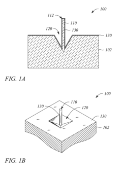
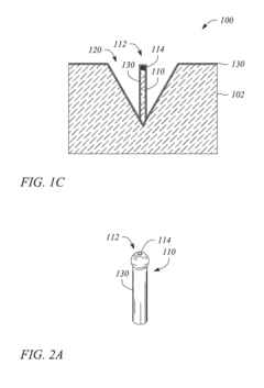
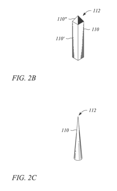
- A method involving the use of a pulsed laser source with a pulse width less than one picosecond to pattern SERS substrates, creating a patterned area with repeated scans and adjusting the separation between scanned lines to match the effective beam waist, combined with a base layer and a Raman signal-enhancing material like gold or silver, to produce substrates with both positive and negative curvature and nanoparticles, enhancing the Raman signal for EV detection.
Surface enhanced raman spectroscopy employing a nanorod in a surface indentation
PatentInactiveUS9080980B2
Innovation
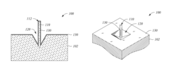
- Incorporating a nanorod into a surface indentation on a substrate, which enhances the Raman scattering signal by launching plasmons and focusing the electromagnetic field at the nanorod tip and its interface with the indentation, achieving a Raman enhancement factor exceeding 10^11.
Environmental Impact of SERS Substrate Manufacturing
The manufacturing processes for Surface-Enhanced Raman Spectroscopy (SERS) substrates used in semiconductor coatings present significant environmental considerations that warrant careful examination. Traditional fabrication methods often involve hazardous chemicals such as strong acids, organic solvents, and heavy metal precursors that pose substantial risks to ecosystems when improperly managed. Particularly concerning are gold and silver nanoparticles—common materials in SERS substrates—which can persist in the environment and potentially bioaccumulate in aquatic organisms.
Water consumption represents another critical environmental factor, with nanofabrication processes typically requiring ultrapure water in volumes significantly exceeding those of conventional manufacturing. A single semiconductor facility may consume millions of gallons daily, placing considerable pressure on local water resources, especially in regions already experiencing water scarcity.
Energy requirements for SERS substrate production are similarly intensive. Techniques such as electron-beam lithography, chemical vapor deposition, and plasma etching demand substantial electrical power, contributing to carbon emissions when sourced from non-renewable energy. Recent industry analyses suggest that advanced nanofabrication facilities can consume energy equivalent to that of small municipalities.
Waste management challenges are particularly acute in this sector. The production process generates various waste streams containing nanomaterials, acids, bases, and metal-contaminated solutions. These require specialized treatment protocols that exceed conventional industrial waste management capabilities, as standard municipal systems cannot effectively remove nanoscale contaminants.
Regulatory frameworks addressing these environmental impacts remain inconsistent globally. While regions like the European Union have implemented the REACH regulation to govern chemical usage and the RoHS directive to limit hazardous substances, many developing nations where manufacturing may be outsourced lack comparable environmental protections.
Encouragingly, sustainable alternatives are emerging within the industry. Green chemistry approaches utilizing ionic liquids as replacements for conventional solvents, biologically-inspired synthesis methods employing plant extracts, and closed-loop manufacturing systems that recycle process chemicals all demonstrate promising reductions in environmental footprint. Additionally, several leading manufacturers have begun implementing ISO 14001 environmental management systems specifically tailored to nanomaterial production.
The life cycle assessment (LCA) of SERS substrates reveals that environmental impacts extend beyond manufacturing to include raw material extraction, transportation, use phase, and end-of-life disposal. Complete cradle-to-grave analysis indicates that improvements in manufacturing efficiency alone are insufficient without corresponding advances in responsible sourcing and recycling technologies.
Standardization and Quality Control in SERS Applications
Standardization and quality control represent critical challenges in the widespread adoption of SERS technology for semiconductor coating applications. The inherent variability in SERS substrate fabrication processes has historically limited reproducibility across different laboratories and manufacturing facilities, creating significant barriers to industrial implementation.
Current standardization efforts focus on establishing universal protocols for substrate preparation, measurement conditions, and data analysis. Organizations such as ASTM International and the International Organization for Standardization (ISO) have begun developing specific guidelines for SERS measurements, though comprehensive standards for semiconductor coating applications remain underdeveloped. These emerging standards address critical parameters including substrate roughness, nanoparticle size distribution, and enhancement factor quantification.
Quality control methodologies for SERS substrates in semiconductor coatings have evolved significantly in recent years. Advanced characterization techniques including electron microscopy, atomic force microscopy, and spectroscopic ellipsometry now enable precise evaluation of substrate morphology and optical properties. Real-time monitoring systems incorporating machine learning algorithms can detect deviations during manufacturing processes, allowing for immediate corrective actions.
Statistical process control (SPC) implementation has proven particularly valuable for maintaining consistency in large-scale SERS substrate production. By establishing control charts for critical parameters such as signal intensity, peak position, and background noise levels, manufacturers can identify process drift before it impacts product performance. Reference materials containing known concentrations of target analytes serve as calibration standards, enabling quantitative comparison across different production batches.
Interlaboratory comparison studies have highlighted the importance of standardized measurement protocols. Recent round-robin tests involving multiple research institutions demonstrated that measurement variability could be reduced by over 60% through implementation of standardized sample preparation and data collection procedures. These findings underscore the necessity of establishing industry-wide best practices.
Future standardization efforts must address emerging challenges in semiconductor coating applications, particularly regarding substrate stability under varying environmental conditions and compatibility with existing semiconductor manufacturing processes. Development of certified reference materials specifically designed for semiconductor-relevant analytes will facilitate more accurate calibration and validation procedures, ultimately accelerating industrial adoption of SERS-based sensing technologies in semiconductor manufacturing environments.
Unlock deeper insights with Patsnap Eureka Quick Research — get a full tech report to explore trends and direct your research. Try now!
Generate Your Research Report Instantly with AI Agent
Supercharge your innovation with Patsnap Eureka AI Agent Platform!