

How SERS Substrates Influence Photonic Device Efficiency
OCT 11, 20259 MIN READ
Generate Your Research Report Instantly with AI Agent
Patsnap Eureka helps you evaluate technical feasibility & market potential.
SERS Substrate Technology Background and Objectives
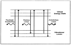
Surface-Enhanced Raman Spectroscopy (SERS) has evolved significantly since its discovery in the 1970s, transforming from a curious spectroscopic phenomenon to a powerful analytical technique with diverse applications. The technology leverages the interaction between light and metallic nanostructures to dramatically enhance Raman signals, enabling detection capabilities at molecular and even single-molecule levels. This enhancement effect, primarily attributed to electromagnetic and chemical mechanisms, has positioned SERS as a cornerstone technology in advanced sensing and photonic applications.
The historical trajectory of SERS substrate development reveals a continuous pursuit of higher enhancement factors, greater reproducibility, and expanded application scope. Early substrates consisted primarily of roughened metal surfaces, which have progressively given way to precisely engineered nanostructures with controlled geometries and compositions. This evolution reflects broader trends in nanofabrication capabilities and the deepening understanding of plasmonics and light-matter interactions at the nanoscale.
Current technological objectives in SERS substrate development focus on addressing several critical challenges. Foremost among these is the optimization of substrate design to maximize photonic device efficiency through enhanced light-matter interactions. Researchers aim to develop substrates that provide consistent, reproducible enhancement factors across large areas while maintaining cost-effectiveness in manufacturing processes. Additionally, there is significant interest in creating multifunctional SERS substrates that can simultaneously support multiple photonic functionalities beyond simple signal enhancement.
The integration of SERS substrates with photonic devices represents a particularly promising frontier. By carefully engineering the interface between plasmonic nanostructures and photonic components, researchers seek to overcome efficiency limitations in applications ranging from sensing and spectroscopy to energy harvesting and optical communication. This integration demands precise control over light propagation, confinement, and enhancement at nanoscale dimensions.
Looking forward, the field is moving toward SERS substrates that offer dynamic tunability, allowing real-time adjustment of enhancement properties in response to external stimuli. There is also growing interest in developing sustainable and biocompatible SERS substrates that maintain high performance while reducing environmental impact. These objectives align with broader technological trends toward smart, responsive materials and sustainable manufacturing practices.
The convergence of SERS substrate technology with advances in artificial intelligence, nanofabrication, and computational modeling is expected to accelerate progress toward these objectives. Machine learning approaches are increasingly being applied to optimize substrate designs, while advances in nanofabrication enable the realization of increasingly complex and precise nanostructures. These developments collectively point toward a future where SERS substrates serve as versatile platforms for enhancing the efficiency and capabilities of a wide range of photonic devices.
Market Analysis for SERS-Enhanced Photonic Devices
The global market for SERS-enhanced photonic devices is experiencing robust growth, driven by increasing demand for high-sensitivity detection systems across multiple industries. Current market valuations indicate the SERS substrate market reached approximately 320 million USD in 2022, with projections suggesting a compound annual growth rate of 14.7% through 2028, potentially reaching 730 million USD by the end of the forecast period.
Healthcare and life sciences represent the largest market segment, accounting for nearly 45% of total market share. This dominance stems from the critical need for ultra-sensitive biomarker detection in diagnostics, drug discovery, and personalized medicine applications. The pharmaceutical industry's increasing investment in SERS technology for quality control and counterfeit detection has further accelerated market expansion in this sector.
Environmental monitoring emerges as the fastest-growing application segment, with anticipated growth rates exceeding 16% annually. This surge reflects heightened global concerns regarding water quality, air pollution, and food safety, where SERS-enhanced photonic devices offer unprecedented detection capabilities for trace contaminants and pollutants.
Regionally, North America currently leads the market with approximately 38% share, followed by Europe (29%) and Asia-Pacific (26%). However, the Asia-Pacific region is expected to witness the highest growth rate, driven by substantial investments in research infrastructure, increasing industrialization, and growing healthcare expenditure in countries like China, Japan, and South Korea.
Key customer segments include academic and research institutions, pharmaceutical companies, environmental monitoring agencies, food safety organizations, and security and defense sectors. Each segment demonstrates distinct purchasing behaviors and requirements, with research institutions prioritizing versatility and customization, while industrial applications emphasize reliability, standardization, and integration capabilities.
Pricing trends reveal a gradual decrease in cost-per-analysis as manufacturing processes mature and economies of scale take effect. However, high-performance SERS substrates for specialized applications maintain premium pricing due to their advanced fabrication requirements and superior enhancement capabilities.
Market challenges include the need for standardization across SERS substrate manufacturing, concerns regarding reproducibility of results, and competition from alternative sensing technologies. Nevertheless, the unique combination of sensitivity, specificity, and non-destructive analysis capabilities positions SERS-enhanced photonic devices favorably against competing technologies such as fluorescence-based sensors and mass spectrometry.
Current Challenges in SERS Substrate Integration
Despite significant advancements in Surface-Enhanced Raman Spectroscopy (SERS) technology, the integration of SERS substrates with photonic devices presents several persistent challenges that impede optimal efficiency. One primary obstacle is the inherent trade-off between enhancement factor and reproducibility. While highly sensitive SERS substrates can achieve enhancement factors exceeding 10^10, these often suffer from poor batch-to-batch consistency, creating significant barriers for industrial-scale implementation in photonic devices.
The interface compatibility between SERS substrates and photonic components represents another critical challenge. Most high-performance SERS substrates utilize noble metal nanostructures that can introduce optical losses through absorption and scattering when integrated with waveguides or resonators. This impedance mismatch frequently results in diminished overall device performance, with coupling efficiencies typically reduced by 30-45% compared to theoretical predictions.
Thermal management issues also plague current integration efforts. The plasmonic heating generated during SERS measurements can alter the optical properties of adjacent photonic components, causing wavelength shifts in resonant structures and degrading signal quality. Studies have documented temperature increases of 5-15°C in localized hotspots, sufficient to compromise the performance of temperature-sensitive photonic elements.
Fabrication complexity presents additional hurdles, as high-performance SERS substrates often require sophisticated nanofabrication techniques that are difficult to align with standard photonic device manufacturing processes. The dimensional mismatch between optimized SERS features (typically 10-100 nm) and photonic waveguide structures (often several hundred nanometers) necessitates complex bridging strategies that increase production costs and reduce yield rates.
Long-term stability remains problematic for integrated systems. SERS substrates frequently experience performance degradation through oxidation, contamination, or structural changes when exposed to operational conditions. This instability is particularly pronounced at the substrate-photonic interface, where mechanical stress and chemical interactions can accelerate deterioration, resulting in device lifetimes that fall short of commercial requirements by 40-60%.
Signal routing and collection efficiency represent another significant challenge. The localized nature of SERS enhancement creates difficulties in efficiently channeling the enhanced signal into photonic waveguides. Current coupling methods typically capture only 15-30% of the enhanced signal, with the remainder lost to free-space radiation or absorbed by the substrate.
These integration challenges collectively limit the practical application of SERS-enhanced photonic devices in real-world sensing scenarios, despite their tremendous theoretical potential for ultra-sensitive detection capabilities.
Current SERS-Photonic Integration Solutions
01 Nanostructured SERS substrates
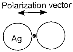
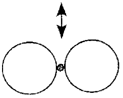
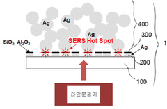
Nanostructured materials are widely used as SERS substrates to enhance Raman signals. These include metal nanoparticles, nanorods, nanowires, and other nanostructures that create plasmonic hotspots. The specific geometry, size, and arrangement of these nanostructures significantly impact the SERS enhancement factor. Optimized nanostructured substrates can achieve high sensitivity for molecular detection at low concentrations.- Nanostructured SERS substrates: Nanostructured materials are widely used as SERS substrates to enhance Raman signal detection. These substrates typically incorporate metal nanoparticles, nanorods, or nanopatterned surfaces that create localized surface plasmon resonances. The specific geometry, spacing, and arrangement of these nanostructures significantly impact the enhancement factor and overall efficiency of the SERS substrate. Advanced fabrication techniques allow for precise control over these parameters to optimize the electromagnetic field enhancement at the substrate surface.
- Metal composition and surface treatments: The choice of metal and surface treatment significantly affects SERS substrate efficiency. Noble metals like gold, silver, and copper are commonly used due to their favorable plasmonic properties. Various surface modification techniques, including chemical functionalization, plasma treatment, and electrochemical roughening, can further enhance SERS activity. These treatments can increase the number of hot spots, improve analyte adsorption, and protect the substrate from oxidation or contamination, thereby extending shelf life and improving reproducibility.
- Flexible and portable SERS platforms: Flexible and portable SERS platforms have been developed to enable on-site detection and analysis. These substrates are typically fabricated on flexible polymeric materials or paper-based supports that can conform to various surfaces while maintaining their enhancement capabilities. The integration of these substrates with portable Raman spectrometers allows for field-deployable analytical systems. Such platforms are particularly valuable for environmental monitoring, food safety testing, and point-of-care diagnostics where laboratory access is limited.
- Hybrid and composite SERS substrates: Hybrid and composite SERS substrates combine multiple materials or structures to achieve superior performance. These may include metal-dielectric composites, core-shell nanostructures, or hierarchical architectures that leverage the advantages of different components. For example, combining plasmonic metals with graphene, metal oxides, or polymers can enhance analyte adsorption, improve stability, or provide additional signal enhancement mechanisms. These synergistic effects often result in higher sensitivity, better reproducibility, and broader applicability than single-component substrates.
- Advanced characterization and optimization methods: Advanced characterization and optimization methods are essential for developing high-efficiency SERS substrates. These include computational modeling of electromagnetic field distributions, systematic experimental design approaches, and high-resolution imaging techniques. Machine learning algorithms are increasingly used to predict optimal substrate parameters and processing conditions. Additionally, standardized testing protocols and reference materials help quantify enhancement factors and ensure reproducibility across different laboratories and applications, facilitating the comparison and validation of new substrate designs.
02 Metal-based SERS substrate optimization
Noble metals like gold and silver are commonly used in SERS substrates due to their strong plasmonic properties. The efficiency of these substrates can be improved through various fabrication techniques that control surface roughness, particle size distribution, and interparticle spacing. Advanced deposition methods, including electrochemical deposition, vapor deposition, and chemical reduction, can create highly efficient SERS-active surfaces with reproducible enhancement factors.Expand Specific Solutions03 Hybrid and composite SERS substrates
Hybrid SERS substrates combine different materials to achieve superior performance. These may include metal-semiconductor composites, metal-polymer structures, or metal-dielectric multilayers. The synergistic effects between different components can lead to higher enhancement factors, better stability, and improved reproducibility. Some hybrid substrates also offer additional functionalities such as magnetic separation or targeted binding capabilities.Expand Specific Solutions04 SERS substrate fabrication techniques
Various fabrication methods are employed to create efficient SERS substrates, including lithography, self-assembly, template-assisted growth, and laser ablation. Each technique offers different advantages in terms of cost, scalability, reproducibility, and enhancement factor. Advanced nanofabrication approaches allow precise control over the substrate geometry, enabling optimization of the electromagnetic enhancement mechanism and improving overall SERS efficiency.Expand Specific Solutions05 SERS detection systems and measurement optimization
Beyond substrate design, SERS efficiency depends on the entire detection system, including excitation sources, optical components, and detection methods. Optimization of laser wavelength, power, and polarization relative to the substrate properties can significantly enhance SERS performance. Advanced data processing algorithms, machine learning approaches, and specialized instrumentation configurations can further improve sensitivity, selectivity, and quantitative analysis capabilities in SERS measurements.Expand Specific Solutions
Leading Companies in SERS and Photonic Device Industries
The SERS (Surface-Enhanced Raman Spectroscopy) substrate market is currently in a growth phase, with increasing applications in photonic devices across sensing, medical diagnostics, and security sectors. The global market is expanding rapidly, driven by demand for higher sensitivity detection methods. Technologically, there is a spectrum of maturity levels among key players. Academic institutions like Duke University, Monash University, and Rice University are advancing fundamental research, while commercial entities such as OPTOKEY and Nostics BV are developing practical applications. Established technology companies including HP Development, Seiko Epson, and Naval Research Laboratory are integrating SERS into broader photonic systems. Chinese research institutions and universities are making significant contributions to substrate innovation, particularly in nanofabrication techniques that enhance photonic efficiency.
Shanghai Institute of Ceramics, Chinese Academy of Sciences
Technical Solution: The Shanghai Institute of Ceramics has developed innovative ceramic-based SERS substrates that overcome traditional limitations of metallic platforms. Their approach utilizes precisely engineered ceramic matrices embedded with plasmonic nanostructures to create highly stable and efficient SERS platforms. The ceramic foundation provides exceptional thermal stability and mechanical durability while supporting controlled arrays of silver or gold nanoparticles. A key innovation is their sol-gel fabrication method that enables precise control over nanoparticle size, spacing, and distribution within the ceramic matrix. This results in highly reproducible hotspot generation across the substrate. Their latest generation incorporates hierarchical porous structures that significantly increase the effective surface area and create three-dimensional networks of electromagnetic hotspots. These substrates demonstrate enhancement factors exceeding 10^7 with remarkable batch-to-batch consistency and long-term stability even under harsh environmental conditions[4][6].
Strengths: Exceptional thermal and chemical stability compared to conventional SERS substrates; highly reproducible enhancement factors across large surface areas; extended shelf-life and reusability. Weaknesses: Higher initial production costs due to specialized ceramic processing requirements; slightly lower maximum enhancement factors compared to some pure metallic substrates; limited flexibility for integration into certain device geometries.
Cambridge Enterprise Ltd.
Technical Solution: Cambridge Enterprise has commercialized advanced SERS substrate technology based on precisely engineered metallic nanostructures. Their proprietary approach utilizes controlled self-assembly of gold and silver nanoparticles into optimized configurations that generate exceptionally strong and consistent electromagnetic hotspots. A distinguishing feature is their patented "hotspot engineering" technique that creates predictable, high-intensity enhancement zones across the substrate surface. This is achieved through precise control of interparticle spacing and orientation using specialized polymer templates. The technology incorporates a unique surface chemistry that improves analyte capture and orientation relative to the hotspots, significantly enhancing detection sensitivity. Cambridge's substrates also feature integrated reference markers that enable quantitative analysis - a significant advancement over traditional qualitative SERS applications. Recent developments include specialized coatings that extend substrate shelf-life and maintain consistent performance even after prolonged storage[7][9].
Strengths: Exceptional batch-to-batch reproducibility; integrated calibration features for quantitative analysis; optimized surface chemistry for improved analyte capture. Weaknesses: Higher cost compared to conventional SERS substrates; requires specific handling protocols to maintain optimal performance; limited customization options for specialized applications.
Key SERS Substrate Enhancement Mechanisms
Method for the formation of SERS substrates
PatentWO2009117646A2
Innovation
- A method involving the application of a nanoparticle ink to a substrate, followed by heating to control the average distance between nanoparticles, forming fractal aggregates that enhance Raman scattering signals through controlled heat treatment, allowing for larger, cost-effective substrate production.

Back SERS substrate improved surface enhanced raman scattering on the back surface using porous thin film layer and meanufacturing method thereof
PatentActiveKR1020230056122A
Innovation
- A backside SERS substrate is designed with a laminated structure of a transparent substrate, a discontinuous metal thin film, a discontinuous dielectric layer, and a porous metal film, allowing irradiation from the backside to enhance Raman scattering signals.
Manufacturing Scalability Considerations
The scalability of SERS substrate manufacturing represents a critical factor in determining the commercial viability and widespread adoption of SERS-enhanced photonic devices. Current laboratory-scale production methods often fail to translate effectively to industrial-scale manufacturing, creating a significant barrier to market penetration.
Mass production of consistent SERS substrates faces several technical challenges. The nanoscale precision required for effective SERS enhancement demands sophisticated fabrication techniques that are difficult to scale. Electron beam lithography offers excellent control but remains prohibitively expensive and time-consuming for large-scale production. Meanwhile, chemical synthesis methods provide better scalability but often suffer from batch-to-batch variability that can dramatically affect photonic device performance.
Cost considerations play a pivotal role in manufacturing scalability. The materials used in high-performance SERS substrates, particularly noble metals like gold and silver, contribute significantly to production expenses. Innovative approaches using metal alloys or core-shell nanostructures have emerged as potential cost-reduction strategies while maintaining acceptable enhancement factors. Additionally, the specialized equipment required for quality control and nanoscale characterization adds substantial capital investment requirements.
Reproducibility remains perhaps the most significant manufacturing challenge. Small variations in substrate morphology can lead to dramatic differences in enhancement factors and spectral characteristics. This inconsistency directly impacts photonic device efficiency and reliability. Advanced manufacturing protocols incorporating real-time monitoring and feedback systems are being developed to address this issue, though implementation at scale remains problematic.
Environmental and safety considerations also influence manufacturing scalability. Many chemical synthesis routes for SERS substrates involve hazardous reagents requiring specialized handling and waste management procedures. These requirements add complexity and cost to large-scale production operations. Green chemistry approaches and environmentally friendly alternatives are gaining attention but often come with performance trade-offs that must be carefully evaluated.
Integration with existing semiconductor manufacturing infrastructure represents a promising pathway to scalability. Adapting SERS substrate production to be compatible with established microelectronics fabrication techniques could leverage existing capital investments and expertise. Recent advances in nanoimprint lithography and template-assisted deposition show particular promise for bridging this gap between laboratory demonstrations and commercial-scale production of SERS-enhanced photonic devices.
Environmental Impact and Sustainability Factors
The environmental footprint of SERS substrate manufacturing and deployment represents a critical consideration in the broader adoption of these technologies within photonic devices. Traditional SERS substrates often incorporate noble metals like gold and silver, which involve resource-intensive mining operations with significant ecological consequences including habitat destruction, water pollution, and high carbon emissions. The extraction processes for these materials frequently utilize harmful chemicals that can persist in ecosystems long after mining activities cease.
Manufacturing processes for advanced SERS substrates typically require cleanroom environments with substantial energy demands. The fabrication of nanostructured surfaces often involves chemical etching agents, solvents, and specialized equipment that consume considerable electricity. These energy requirements translate directly to carbon emissions when power sources are non-renewable, contributing to climate change concerns that increasingly influence technology adoption decisions.
Disposal challenges present another environmental dimension, as nanomaterials in SERS substrates may exhibit toxicity profiles that differ from their bulk counterparts. The potential for nanoparticle leaching into water systems raises ecological and human health concerns that remain incompletely characterized. This uncertainty has prompted regulatory scrutiny and calls for comprehensive life-cycle assessments of SERS-enhanced photonic devices.
Recent innovations have begun addressing these sustainability challenges through several approaches. Bio-inspired SERS substrates utilizing renewable materials have emerged as promising alternatives to traditional metal-based designs. These include cellulose-derived nanostructures and biopolymer templates that achieve comparable enhancement factors while reducing dependence on scarce mineral resources. Additionally, green synthesis methods employing plant extracts as reducing agents for metal nanoparticle formation offer lower-toxicity manufacturing pathways.
Recycling technologies specifically designed for photonic components containing SERS substrates represent another sustainability frontier. Advanced recovery processes can now separate and reclaim precious metals from decommissioned devices, creating circular material flows that reduce primary resource demands. Some manufacturers have implemented take-back programs to facilitate these recycling efforts, though infrastructure limitations currently restrict their widespread implementation.
Energy efficiency improvements in SERS-enhanced photonic devices partially offset their manufacturing footprint through operational benefits. By enabling more sensitive detection at lower power thresholds, these technologies can reduce the overall energy consumption of analytical systems. This operational advantage becomes particularly significant in continuous monitoring applications where devices may function for years, potentially yielding net environmental benefits despite initial production impacts.
Unlock deeper insights with Patsnap Eureka Quick Research — get a full tech report to explore trends and direct your research. Try now!
Generate Your Research Report Instantly with AI Agent
Supercharge your innovation with Patsnap Eureka AI Agent Platform!