Role of SERS Substrates in Enhancing Photon Efficiency
OCT 11, 20259 MIN READ
Generate Your Research Report Instantly with AI Agent
Patsnap Eureka helps you evaluate technical feasibility & market potential.
SERS Substrate Technology Background and Objectives
Surface-Enhanced Raman Spectroscopy (SERS) has evolved significantly since its discovery in the 1970s, transforming from an interesting optical phenomenon to a powerful analytical technique with applications spanning from biosensing to environmental monitoring. The fundamental principle behind SERS lies in the enhancement of Raman signals through interactions between analyte molecules and nanostructured metallic surfaces, primarily through electromagnetic and chemical enhancement mechanisms. This enhancement can reach factors of 10^6 to 10^14, enabling single-molecule detection capabilities that were previously unattainable with conventional spectroscopic methods.
The technological evolution of SERS substrates has progressed through several distinct phases. Early research focused on roughened metal electrodes and colloidal solutions, while contemporary approaches have advanced to precisely engineered nanostructures with controlled geometries and compositions. This progression reflects the growing understanding of plasmonics and nanofabrication techniques that has occurred in parallel with SERS development.
Current research trends are increasingly focused on optimizing photon efficiency—the ability to maximize the conversion of incident photons into detectable Raman-scattered photons. This optimization represents a critical frontier in SERS technology, as improved photon efficiency directly translates to enhanced sensitivity, reproducibility, and practical applicability across diverse analytical scenarios.
The primary technical objectives in SERS substrate development center on several key parameters: enhancement factor maximization, reproducibility improvement, stability enhancement, and cost-effective manufacturing scalability. Researchers aim to design substrates that can provide consistent signal enhancement across large surface areas while maintaining molecular specificity and minimizing background interference.
Emerging approaches include the development of hybrid plasmonic-photonic structures, three-dimensional hierarchical substrates, and flexible SERS platforms for in-situ applications. These innovations seek to address the limitations of traditional substrates by expanding the effective enhancement volume and improving light-matter interactions at the nanoscale.
The ultimate goal of current SERS substrate research is to bridge the gap between laboratory demonstrations and practical real-world applications. This transition requires substrates that not only deliver exceptional enhancement performance but also offer reliability, ease of use, and compatibility with existing analytical workflows and instrumentation.
Understanding the fundamental role of SERS substrates in photon efficiency enhancement is essential for guiding future technological developments. By systematically exploring the relationship between substrate properties and enhancement mechanisms, researchers can establish design principles that will enable the next generation of high-performance SERS platforms with transformative capabilities for analytical science and technology.
Market Analysis for Enhanced Photon Efficiency Applications
The global market for enhanced photon efficiency applications is experiencing robust growth, driven primarily by advancements in Surface-Enhanced Raman Spectroscopy (SERS) substrate technologies. Current market valuations indicate that the SERS technology market reached approximately 1.2 billion USD in 2022, with projections suggesting a compound annual growth rate of 10-12% through 2028.
Key market segments benefiting from enhanced photon efficiency include biomedical diagnostics, environmental monitoring, food safety testing, pharmaceutical development, and security applications. The biomedical diagnostics sector represents the largest market share at roughly 35%, followed by pharmaceutical applications at 25%. This distribution reflects the critical importance of high-sensitivity detection capabilities in healthcare-related fields.
Regionally, North America dominates the market with approximately 40% share, followed by Europe (30%) and Asia-Pacific (25%). However, the Asia-Pacific region is demonstrating the fastest growth rate, particularly in China, Japan, and South Korea, where significant investments in research infrastructure and manufacturing capabilities are occurring.
Customer demand is increasingly focused on SERS substrates that offer higher enhancement factors, better reproducibility, and cost-effective manufacturing processes. End-users are willing to pay premium prices for substrates that can consistently deliver enhancement factors above 10^8, particularly for trace detection applications in clinical diagnostics and environmental monitoring.
Market adoption barriers include high initial equipment costs, technical expertise requirements, and standardization challenges. The average cost of high-performance SERS systems ranges from 50,000 to 150,000 USD, limiting widespread adoption in smaller laboratories and developing regions.
Competitive analysis reveals that the market structure is relatively concentrated, with the top five players controlling approximately 65% of the global market. These leaders have established strong patent portfolios around core substrate technologies. However, emerging startups are gaining traction with innovative approaches to substrate fabrication that promise lower costs and improved performance metrics.
Future market growth will be significantly influenced by technological advancements in substrate design, particularly those addressing current limitations in reproducibility and stability. The development of standardized performance metrics and testing protocols will also play a crucial role in market expansion by increasing customer confidence and enabling more direct product comparisons.
Current SERS Substrate Limitations and Technical Challenges
Despite significant advancements in Surface-Enhanced Raman Spectroscopy (SERS) technology, current SERS substrates face several critical limitations that hinder their widespread application and commercial viability. The fundamental challenge remains achieving consistent and reproducible enhancement factors across the substrate surface. Conventional substrates often exhibit "hot spots" - isolated areas of extremely high enhancement surrounded by regions of minimal activity, resulting in signal variability that can exceed several orders of magnitude.
Scalable manufacturing presents another significant hurdle. While laboratory-scale production of high-performance SERS substrates is achievable, translating these processes to industrial-scale manufacturing while maintaining quality and performance remains problematic. This manufacturing gap directly impacts cost-effectiveness and accessibility of SERS technology across various sectors.
Stability issues further complicate SERS substrate utility. Many high-performance substrates demonstrate rapid degradation under normal operating conditions, with sensitivity to environmental factors such as oxidation, contamination, and mechanical stress. This instability severely limits shelf-life and reliability in real-world applications, particularly in field-deployable systems where controlled environments cannot be guaranteed.
The photon efficiency of current substrates represents a critical technical bottleneck. Most SERS substrates convert only a small fraction of incident photons into useful Raman-scattered signals. This inefficiency necessitates higher laser powers or longer acquisition times, which can damage sensitive samples or reduce throughput in analytical applications.
Substrate specificity also presents challenges, as most current designs are optimized for specific molecular targets or wavelength ranges. This specialization limits versatility across different analytical scenarios and increases costs for laboratories requiring multiple substrate types for comprehensive analysis capabilities.
Biocompatibility remains problematic for in vivo or biological applications. Many high-performance SERS substrates incorporate materials with potential toxicity or utilize surface chemistries incompatible with biological systems. This limitation significantly restricts the expansion of SERS into biomedical diagnostics and monitoring applications.
From a technical perspective, the trade-off between enhancement factor and background signal presents an ongoing challenge. Substrates that provide exceptional enhancement often generate higher background signals, reducing the signal-to-noise ratio and complicating data analysis, particularly for trace detection applications.
The gap between theoretical models and practical performance further complicates development efforts. Current computational models fail to accurately predict real-world substrate performance across diverse conditions, hampering rational design approaches and necessitating extensive empirical optimization.
Contemporary SERS Substrate Design Approaches
01 Nanostructured SERS substrates for enhanced photon efficiency
Nanostructured materials are used as SERS substrates to enhance photon efficiency. These substrates typically incorporate metallic nanoparticles or nanostructures with specific geometries that create localized surface plasmon resonances, significantly amplifying the Raman signal. The careful design of nanostructure size, shape, and spacing allows for optimization of the electromagnetic field enhancement, resulting in improved SERS detection sensitivity and photon collection efficiency.- Nanostructured SERS substrates for enhanced photon efficiency: Nanostructured materials are used as SERS substrates to enhance photon efficiency. These substrates typically incorporate metallic nanoparticles, nanopillars, or nanogaps that create localized surface plasmon resonances, significantly amplifying the Raman signal. The specific geometry and arrangement of these nanostructures can be optimized to maximize the electromagnetic field enhancement and improve the overall photon collection efficiency in SERS measurements.
- Metal-enhanced SERS substrates: Metal-enhanced SERS substrates utilize noble metals (primarily gold and silver) to improve photon efficiency through plasmonic effects. These substrates are designed with specific metal film thicknesses, particle sizes, and distributions to optimize the electromagnetic field enhancement. Advanced fabrication techniques ensure uniform coverage and reproducible hot spots, leading to consistent signal enhancement and improved detection limits for various analytes.
- Hybrid and composite SERS substrates: Hybrid and composite SERS substrates combine different materials to achieve superior photon efficiency. These substrates often integrate metallic nanostructures with semiconductors, polymers, or 2D materials like graphene. The synergistic effects between these materials can lead to enhanced light absorption, improved energy transfer, and reduced fluorescence background, resulting in higher sensitivity and better signal-to-noise ratios in SERS measurements.
- Flexible and adaptable SERS platforms: Flexible and adaptable SERS platforms are designed to maintain high photon efficiency across various sample types and measurement conditions. These substrates can be adjusted or tuned to optimize performance for specific analytes or environments. Some designs incorporate movable components, adjustable surface properties, or responsive materials that can be modified in real-time to maximize signal enhancement and improve detection capabilities.
- Advanced fabrication techniques for high-efficiency SERS substrates: Advanced fabrication techniques are employed to create SERS substrates with exceptional photon efficiency. These methods include lithography, self-assembly, template-assisted growth, and laser processing to produce precisely controlled nanostructures with optimal plasmonic properties. The fabrication processes focus on creating reproducible hot spots, uniform enhancement factors, and stable substrates that maintain their performance over time, enabling reliable quantitative analysis and improved detection limits.
02 Metal-enhanced SERS substrates for photon efficiency improvement
Metal-enhanced SERS substrates utilize specific metals (typically gold, silver, or copper) to improve photon efficiency through plasmonic effects. These substrates are engineered with precise metal layer thicknesses and compositions to maximize the electromagnetic field enhancement at the substrate surface. Advanced fabrication techniques ensure uniform metal deposition and controlled surface roughness, which are critical factors in achieving consistent and high photon efficiency across the entire substrate area.Expand Specific Solutions03 Novel fabrication methods for high-efficiency SERS substrates
Innovative fabrication methods are developed to create SERS substrates with superior photon efficiency. These methods include lithographic techniques, self-assembly processes, template-assisted growth, and chemical etching approaches. The fabrication processes are designed to produce substrates with precise control over surface morphology, creating reproducible hot spots that maximize the enhancement of Raman signals. These advanced manufacturing techniques enable the production of substrates with consistent performance and high photon collection efficiency.Expand Specific Solutions04 Hybrid materials for optimized SERS photon efficiency
Hybrid materials combining different components are utilized to optimize SERS photon efficiency. These substrates often incorporate combinations of metals with semiconductors, polymers, or other functional materials to create synergistic effects. The hybrid approach allows for tailoring of both the electromagnetic and chemical enhancement mechanisms in SERS, resulting in improved photon collection and signal amplification. Additionally, these materials can offer advantages such as improved stability, biocompatibility, or specific target molecule affinity.Expand Specific Solutions05 Detection systems optimizing SERS substrate photon efficiency
Advanced detection systems are designed to maximize the photon efficiency of SERS substrates. These systems incorporate optimized optical components, specialized light sources, and sensitive detectors to efficiently collect and process the enhanced Raman signals. Innovations include confocal arrangements, fiber-optic probes, integrated microfluidics, and automated signal processing algorithms. These detection systems work in concert with the SERS substrates to achieve maximum photon collection efficiency and signal-to-noise ratio, enabling ultra-sensitive molecular detection.Expand Specific Solutions
Leading Companies and Research Institutions in SERS Technology
The SERS substrate market is currently in a growth phase, characterized by increasing research activity and commercial applications. The technology enhances photon efficiency in spectroscopy, enabling ultra-sensitive detection capabilities. The market is expanding with an estimated value of several hundred million dollars, driven by applications in biosensing, chemical detection, and medical diagnostics. Academic institutions like Duke University, Penn State Research Foundation, and Monash University are leading fundamental research, while commercial players including HP Development, Panasonic Holdings, and Atmel Corp. are developing practical applications. The technology maturity varies across sectors, with established players focusing on standardization and emerging companies exploring novel substrate materials and fabrication techniques to improve sensitivity and reproducibility.
Duke University
Technical Solution: Duke University has developed advanced SERS substrates using plasmonic nanostructures with precisely controlled geometries. Their approach involves creating highly ordered arrays of silver and gold nanoparticles with optimized interparticle spacing to generate intense electromagnetic "hot spots" that significantly enhance Raman signals. The university's researchers have pioneered the use of template-directed self-assembly techniques to create reproducible SERS substrates with enhancement factors exceeding 10^8 [1]. Additionally, they've developed novel core-shell nanostructures that combine the plasmonic properties of noble metals with the stability and functionality of other materials, allowing for targeted molecular detection with improved photon efficiency [3]. Their recent work includes the integration of these SERS substrates with microfluidic platforms for real-time sensing applications in biological and environmental monitoring.
Strengths: Exceptional control over nanostructure geometry leading to reproducible and quantifiable enhancement factors; excellent integration with microfluidic systems for practical applications. Weaknesses: Higher production costs compared to simpler substrates; requires specialized equipment for fabrication; some designs may have limited shelf-life due to oxidation of metallic nanostructures.
The Board of Trustees of the University of Illinois
Technical Solution: The University of Illinois has developed innovative SERS substrates using nanoporous metallic films with hierarchical structures. Their approach combines top-down lithography with bottom-up self-assembly to create substrates with multi-scale roughness features that maximize electromagnetic field enhancement. The university's research team has pioneered the use of block copolymer templating to create highly ordered arrays of gold nanocavities with controlled dimensions, achieving enhancement factors of 10^6-10^9 consistently across large areas [2]. They've also developed novel flexible SERS substrates on polymer backings that maintain enhancement properties while conforming to irregular surfaces, enabling new applications in wearable sensing and point-of-care diagnostics [4]. Recent innovations include the incorporation of stimuli-responsive polymers that can modulate the SERS enhancement through controlled swelling and collapse, providing tunable sensing capabilities for different analyte environments.
Strengths: Excellent reproducibility across large substrate areas; innovative flexible designs enable new application domains; hierarchical structures provide multiple enhancement mechanisms. Weaknesses: Complex fabrication processes may limit mass production; some designs show performance degradation after repeated use; optimization required for specific target molecules.
Critical Patents and Breakthroughs in SERS Substrate Engineering
Surface-enhanced raman spectroscopy substrate for arsenic sensing in groundwater
PatentActiveUS9057705B2
Innovation
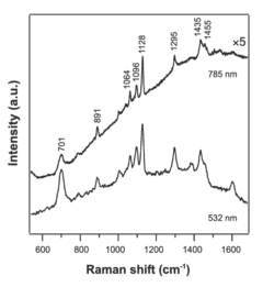
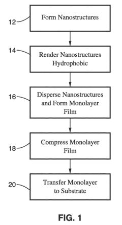
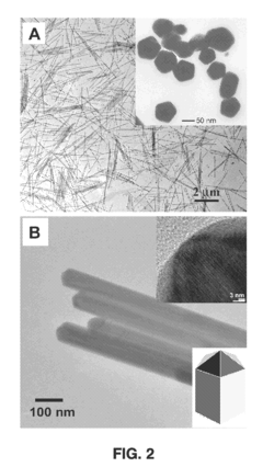
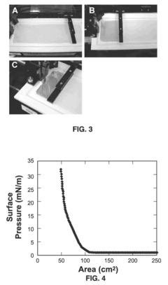
- The Langmuir-Blodgett technique is adapted to assemble monolayers of nanostructures by surface functionalization, allowing for the formation of ordered monolayers of silver nanowires with controlled shapes, such as cube-shaped, plate-shaped, rod-shaped, and hexagon-shaped nanostructures, and their subsequent compression to create aligned, close-packed arrays that function as surface-enhanced Raman spectroscopy (SERS) substrates.
Surface enhanced Raman spectroscopy (SERS) substrates exhibiting uniform high enhancement and stability
PatentInactiveUS7450227B2
Innovation
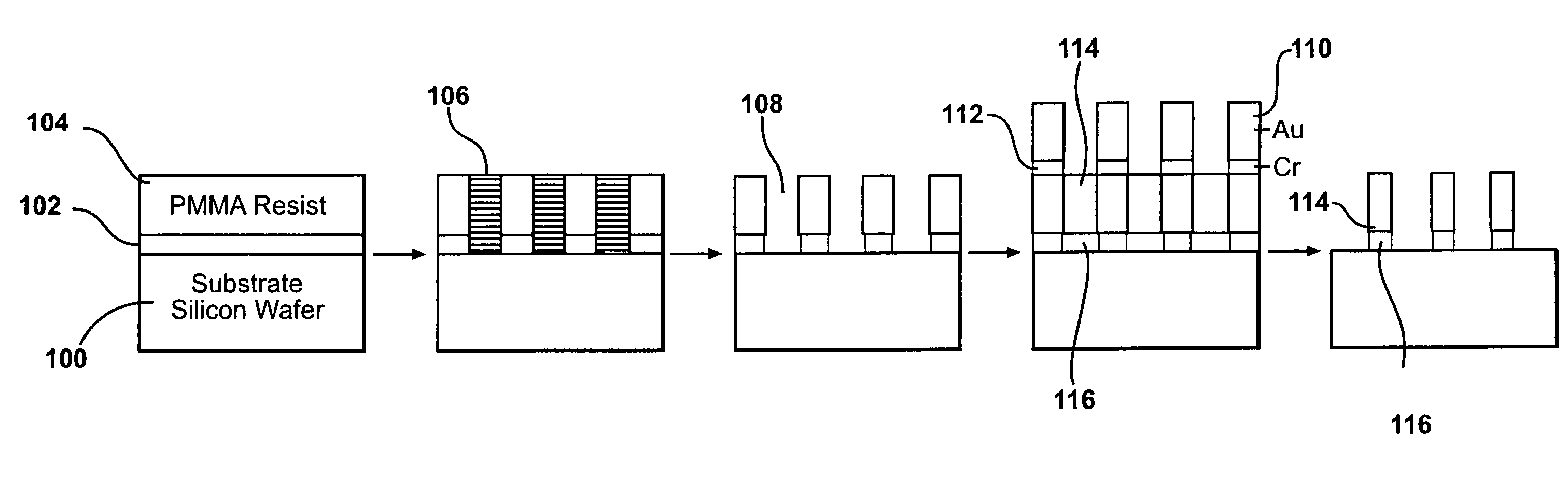
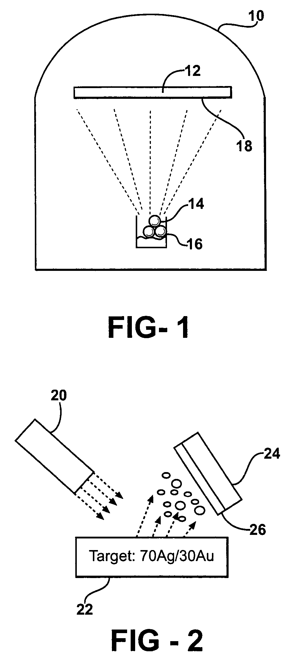
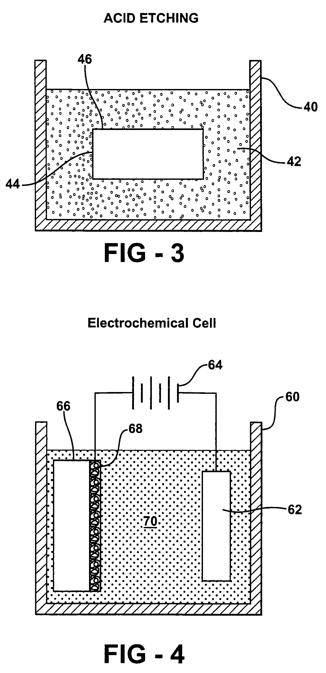
- The development of porous metal substrates, specifically gold substrates created by depositing a gold-silver alloy film and removing the silver through acid etching or electrochemical roughening, resulting in a textured surface that enhances SERS signals uniformly and stably.
Materials Science Considerations for Advanced SERS Substrates
The selection of appropriate materials for Surface-Enhanced Raman Spectroscopy (SERS) substrates is critical for maximizing photon efficiency and achieving optimal sensing performance. Noble metals, particularly gold and silver, remain the predominant materials due to their exceptional plasmonic properties in the visible to near-infrared spectrum. These metals exhibit strong localized surface plasmon resonance (LSPR) effects, which significantly enhance the electromagnetic field around nanostructures and consequently amplify Raman signals.
Recent advances in materials science have expanded the repertoire of SERS substrate compositions beyond traditional noble metals. Aluminum has emerged as a cost-effective alternative with plasmonic properties extending into the ultraviolet region, enabling detection of molecules with electronic transitions in this spectral range. Additionally, hybrid materials combining noble metals with semiconductors or dielectric materials have demonstrated enhanced stability and tunable optical properties.
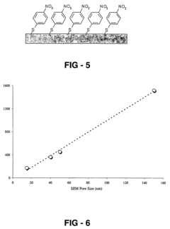
Nanostructure morphology plays a decisive role in SERS enhancement. Controlled fabrication of nanogaps, sharp tips, and edges creates "hot spots" where electromagnetic field enhancement is maximized. Research indicates that gaps between nanoparticles of 1-2 nm can produce enhancement factors exceeding 10^10, enabling single-molecule detection capabilities. The precise engineering of these nanoscale features requires sophisticated fabrication techniques such as electron-beam lithography, template-assisted synthesis, and self-assembly methods.
Surface chemistry modifications represent another critical dimension in SERS substrate development. Functionalization with specific molecular linkers can improve target analyte capture efficiency and orientation, optimizing the interaction between the analyte and the enhanced electromagnetic field. Moreover, surface treatments can prevent aggregation of nanoparticles and extend the shelf-life of SERS substrates, addressing practical implementation challenges.
Substrate stability under various environmental conditions remains a significant materials science challenge. Silver nanostructures, while offering superior enhancement factors compared to gold, are susceptible to oxidation and degradation. Protective coatings using ultrathin layers of alumina or silica have been developed to mitigate these issues without significantly compromising enhancement factors.
Emerging research directions include the development of flexible SERS substrates on polymer supports for wearable sensing applications, and environmentally responsive "smart" SERS substrates that can modulate their enhancement properties in response to external stimuli. These innovations expand the application scope of SERS technology beyond traditional laboratory settings into point-of-care diagnostics and environmental monitoring.
Recent advances in materials science have expanded the repertoire of SERS substrate compositions beyond traditional noble metals. Aluminum has emerged as a cost-effective alternative with plasmonic properties extending into the ultraviolet region, enabling detection of molecules with electronic transitions in this spectral range. Additionally, hybrid materials combining noble metals with semiconductors or dielectric materials have demonstrated enhanced stability and tunable optical properties.
Nanostructure morphology plays a decisive role in SERS enhancement. Controlled fabrication of nanogaps, sharp tips, and edges creates "hot spots" where electromagnetic field enhancement is maximized. Research indicates that gaps between nanoparticles of 1-2 nm can produce enhancement factors exceeding 10^10, enabling single-molecule detection capabilities. The precise engineering of these nanoscale features requires sophisticated fabrication techniques such as electron-beam lithography, template-assisted synthesis, and self-assembly methods.
Surface chemistry modifications represent another critical dimension in SERS substrate development. Functionalization with specific molecular linkers can improve target analyte capture efficiency and orientation, optimizing the interaction between the analyte and the enhanced electromagnetic field. Moreover, surface treatments can prevent aggregation of nanoparticles and extend the shelf-life of SERS substrates, addressing practical implementation challenges.
Substrate stability under various environmental conditions remains a significant materials science challenge. Silver nanostructures, while offering superior enhancement factors compared to gold, are susceptible to oxidation and degradation. Protective coatings using ultrathin layers of alumina or silica have been developed to mitigate these issues without significantly compromising enhancement factors.
Emerging research directions include the development of flexible SERS substrates on polymer supports for wearable sensing applications, and environmentally responsive "smart" SERS substrates that can modulate their enhancement properties in response to external stimuli. These innovations expand the application scope of SERS technology beyond traditional laboratory settings into point-of-care diagnostics and environmental monitoring.
Standardization and Reproducibility Issues in SERS Technology
Despite significant advancements in Surface-Enhanced Raman Spectroscopy (SERS) technology, standardization and reproducibility remain critical challenges that hinder its widespread adoption in commercial applications. The variability in SERS substrate performance directly impacts photon efficiency and signal enhancement, creating obstacles for consistent analytical results across different laboratories and experimental conditions.
One of the primary standardization issues lies in substrate fabrication processes. Different manufacturing methods—from chemical synthesis to nanolithography—produce substrates with varying hot spot densities and enhancement factors. This inconsistency makes it difficult to establish universal protocols for SERS measurements, as the same analyte can generate significantly different signal intensities depending on the substrate used.
The lack of standardized characterization metrics further complicates the situation. While enhancement factor (EF) is commonly used to evaluate SERS substrate performance, calculation methods vary widely across research groups. Some researchers focus on average enhancement across the entire substrate surface, while others emphasize maximum enhancement at hot spots, leading to incomparable results in literature.
Environmental factors introduce additional reproducibility challenges. Substrate performance can be affected by humidity, temperature, and storage conditions, causing degradation over time. This temporal instability means that measurements taken with the same substrate may yield different results depending on when they are conducted, further complicating cross-laboratory validation.
Batch-to-batch variation represents another significant hurdle. Even substrates manufactured using identical processes can exhibit performance differences due to subtle variations in raw materials or environmental conditions during fabrication. This inconsistency makes it difficult for researchers to replicate results and for industries to implement SERS in quality control applications.
Several initiatives are underway to address these challenges. International organizations like ASTM International and ISO are working to develop standardized protocols for SERS substrate characterization and measurement procedures. Additionally, reference materials with known Raman cross-sections are being developed to calibrate enhancement factors across different laboratories.
Technological solutions are also emerging, including automated substrate fabrication systems that minimize human error and improve batch consistency. Some manufacturers are implementing rigorous quality control measures, including statistical process control and comprehensive substrate characterization before distribution, to ensure more consistent photon efficiency enhancement.
Unlock deeper insights with Patsnap Eureka Quick Research — get a full tech report to explore trends and direct your research. Try now!
Generate Your Research Report Instantly with AI Agent
Supercharge your innovation with Patsnap Eureka AI Agent Platform!