Time-Of-Flight On-Chip Processing: Histogramming, SPAD Pile-Up And QoS
SEP 22, 202510 MIN READ
Generate Your Research Report Instantly with AI Agent
Patsnap Eureka helps you evaluate technical feasibility & market potential.
ToF Processing Background and Objectives
Time-of-Flight (ToF) technology has evolved significantly over the past two decades, transforming from laboratory experiments to mainstream sensing solutions in various industries. The fundamental principle of ToF involves measuring the time taken for light to travel from a source to an object and back to a sensor, enabling precise distance measurement and 3D imaging capabilities. This technology has seen accelerated development particularly since the early 2010s with the introduction of Single-Photon Avalanche Diodes (SPADs) that offer superior sensitivity and timing resolution.
The evolution of ToF systems has been marked by continuous improvements in sensor technology, signal processing algorithms, and integration capabilities. Early ToF systems relied on external processing units to handle the complex calculations required for accurate distance measurement. However, the trend has shifted toward on-chip processing solutions that offer advantages in terms of power efficiency, form factor, and real-time performance.
On-chip processing for ToF applications presents unique challenges and opportunities. Histogramming, a critical function in ToF systems, involves accumulating time-of-arrival data to build statistical distributions that enhance measurement accuracy. Traditional implementations required significant off-chip memory and processing resources, limiting the deployment of ToF in resource-constrained applications such as mobile devices and IoT sensors.
SPAD pile-up effects represent another significant challenge in ToF systems. This phenomenon occurs when multiple photons arrive within the dead time of the SPAD detector, leading to measurement inaccuracies. Advanced on-chip processing techniques are being developed to mitigate these effects through statistical modeling and correction algorithms implemented directly at the sensor level.
Quality of Service (QoS) considerations have become increasingly important as ToF technology finds applications in safety-critical systems such as autonomous vehicles and industrial automation. On-chip QoS monitoring and adaptation mechanisms aim to ensure reliable performance across varying environmental conditions and operational scenarios.
The primary objectives of current research in ToF on-chip processing include reducing power consumption, minimizing latency, improving measurement accuracy, and enhancing system robustness. These objectives align with the broader industry trends toward edge computing and AI-enabled sensing, where processing capabilities are distributed closer to the data source rather than centralized in cloud infrastructure.
Recent technological advancements in semiconductor manufacturing, particularly in terms of process node scaling and 3D integration, have created new opportunities for implementing sophisticated ToF processing pipelines on-chip. These developments are expected to drive the next generation of ToF sensors with unprecedented levels of integration, performance, and energy efficiency.
Market Applications for ToF On-Chip Processing
Time-of-Flight (ToF) on-chip processing technology is rapidly expanding across diverse market sectors, driven by increasing demands for precise depth sensing and 3D imaging capabilities. The automotive industry represents one of the most significant application areas, where ToF sensors with integrated histogramming and pile-up correction enable advanced driver assistance systems (ADAS), autonomous navigation, and in-cabin monitoring. These systems require real-time processing to detect obstacles, pedestrians, and other vehicles with minimal latency, making on-chip processing essential for meeting safety-critical response times.
Consumer electronics constitutes another major market, with ToF technology enhancing smartphone cameras, augmented reality (AR) devices, and gaming consoles. The integration of SPAD (Single-Photon Avalanche Diode) arrays with on-chip histogramming capabilities has revolutionized facial recognition systems, enabling secure authentication even in challenging lighting conditions. Market adoption in this sector is accelerating as manufacturers seek to differentiate their products through enhanced user experiences and improved security features.
Industrial automation represents a growing application domain where ToF sensors with quality-of-service (QoS) guarantees support precise object detection, robotic guidance, and inventory management. The ability to process ToF data directly on-chip significantly reduces bandwidth requirements and power consumption, critical factors in battery-operated industrial IoT devices and autonomous robots operating in remote locations.
Healthcare applications are emerging as a promising frontier, with ToF technology enabling non-contact patient monitoring, gait analysis, and surgical navigation systems. On-chip processing of ToF data ensures patient privacy by performing initial data analysis before sensitive information leaves the device, addressing growing concerns about medical data security while maintaining real-time performance.
Smart infrastructure and smart city applications leverage ToF sensors with on-chip processing for people counting, traffic monitoring, and security systems. The ability to handle SPAD pile-up effects directly on the sensor enables these systems to operate reliably in diverse environmental conditions, from bright daylight to complete darkness, expanding their practical deployment scenarios.
Agricultural and environmental monitoring applications are also adopting ToF technology with on-chip processing for crop analysis, livestock monitoring, and terrain mapping. These applications benefit from the reduced power consumption and enhanced reliability offered by integrated processing solutions, enabling deployment in remote locations with limited connectivity and power resources.
Technical Challenges in ToF Sensor Processing
Time-of-Flight (ToF) sensor processing faces several significant technical challenges that impact the overall performance and reliability of these systems. The primary challenge lies in the accurate processing of photon arrival times, which is crucial for depth measurement precision. Current ToF sensors struggle with temporal resolution limitations, typically ranging from tens to hundreds of picoseconds, which directly affects the depth resolution capabilities of the system.
Histogramming presents a particular challenge in ToF processing as it requires efficient on-chip memory allocation and management. The trade-off between histogram bin resolution and memory requirements creates a bottleneck in system design. Higher temporal resolution demands more memory resources, which increases power consumption and chip area—critical constraints for mobile and embedded applications.
SPAD (Single-Photon Avalanche Diode) pile-up effects represent another major technical hurdle. When multiple photons arrive within a short time window, conventional SPAD sensors can only detect the first photon, leading to measurement bias toward shorter distances. This statistical distortion becomes particularly problematic in high ambient light conditions or when measuring objects with varying reflectivity properties.
The Quality of Service (QoS) management in ToF systems introduces additional complexity. Maintaining consistent performance across varying environmental conditions (bright sunlight to low light) requires adaptive processing algorithms. Current solutions struggle to dynamically adjust parameters such as integration time, bias voltage, and filtering thresholds without introducing artifacts or measurement discontinuities.
Noise management represents a persistent challenge in ToF sensor processing. Dark count noise, afterpulsing, and crosstalk between SPAD pixels contaminate the time-of-arrival measurements. While cooling systems can reduce thermal noise, they add cost and complexity, making them impractical for consumer applications.
Power efficiency remains a critical constraint, particularly for battery-operated devices. The computational demands of real-time histogramming and pile-up correction algorithms require significant processing resources. Current on-chip processing solutions must balance processing sophistication against power consumption, often resulting in compromised accuracy or frame rates.
Data bandwidth limitations between the sensor and processing units create bottlenecks in system performance. Full histogram data from high-resolution ToF arrays can exceed practical data transfer rates, necessitating on-chip data reduction techniques that may discard potentially valuable information.
Finally, calibration complexity poses significant challenges for mass production. ToF sensors require sophisticated calibration procedures to account for pixel-to-pixel variations, temperature drift, and aging effects. Developing robust, efficient calibration methods that can be applied in production environments remains an ongoing challenge for the industry.
Current On-Chip Histogramming Solutions
01 On-chip histogramming for Time-of-Flight measurements
On-chip histogramming techniques are implemented in Time-of-Flight (ToF) sensors to efficiently process and analyze photon arrival time data. These systems integrate histogram generation directly on the sensor chip, reducing data transfer requirements and enabling real-time processing. The histogramming circuits accumulate time-correlated photon events into bins, creating statistical distributions that can be used for distance measurement and object detection with improved efficiency and reduced latency.- On-chip histogramming for Time-of-Flight measurements: On-chip histogramming techniques enable efficient processing of Time-of-Flight (ToF) data directly on the sensor chip. This approach reduces data bandwidth requirements by accumulating time-of-arrival measurements into histograms before data transfer. The implementation includes dedicated hardware for binning photon detection events according to their arrival times, allowing for real-time distance measurement processing. These systems often incorporate parallel processing architectures to handle high-speed photon counting while maintaining timing accuracy.
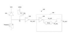
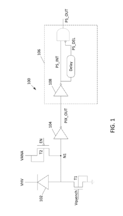
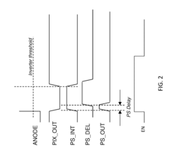
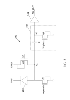
- SPAD pile-up compensation and mitigation techniques: Single-Photon Avalanche Diode (SPAD) sensors face pile-up effects when multiple photons arrive within the dead time of the detector, causing measurement distortions. Advanced compensation algorithms and circuit designs can mitigate these effects by implementing statistical corrections, adaptive timing windows, or multiple SPAD arrays operating in parallel. Some implementations use time-gated operation or specialized quenching circuits to reduce dead time and increase the dynamic range of photon detection, improving measurement accuracy in high-flux environments.
- Quality of Service (QoS) optimization for ToF systems: Quality of Service mechanisms in Time-of-Flight systems dynamically balance measurement accuracy, power consumption, and processing speed based on application requirements. These systems implement adaptive sampling rates, variable resolution modes, and configurable processing pipelines to optimize performance under different operating conditions. QoS controllers can adjust parameters such as integration time, histogram bin width, or processing depth based on scene complexity, ambient light conditions, or application-specific accuracy requirements, ensuring optimal resource utilization.
- Integrated ToF sensor and processing architectures: Advanced ToF systems integrate sensing and processing elements on a single chip to minimize latency and power consumption. These architectures combine SPAD arrays, timing circuits, and digital processing units in compact form factors suitable for mobile and embedded applications. The integration enables direct coupling between photon detection and time measurement circuits, reducing noise and improving timing resolution. Some designs incorporate programmable processing elements that can be reconfigured for different measurement modes or applications, providing flexibility while maintaining high performance.
- Multi-modal ToF data processing techniques: Multi-modal processing techniques combine ToF measurements with complementary sensing modalities or processing approaches to enhance measurement robustness. These systems may fuse data from multiple wavelengths, combine direct and indirect ToF methods, or integrate depth and intensity information for improved scene understanding. Advanced implementations use machine learning algorithms to extract features from raw histogram data, enabling applications such as object recognition, motion tracking, or material classification based on photon timing information. This approach enhances the versatility and reliability of ToF systems in challenging environments.
02 SPAD pile-up compensation and mitigation techniques
Single-Photon Avalanche Diode (SPAD) sensors face pile-up effects when multiple photons arrive within the dead time of the detector, leading to measurement distortions. Advanced compensation algorithms and circuit designs are implemented to mitigate these effects, including statistical correction methods, dynamic dead time adjustment, and multi-SPAD arrays with time-interleaved operation. These techniques improve the linearity and dynamic range of ToF measurements, particularly in high ambient light conditions or when measuring reflective surfaces.Expand Specific Solutions03 Quality of Service (QoS) optimization for ToF systems
Quality of Service mechanisms in Time-of-Flight systems dynamically adjust sensor parameters based on environmental conditions and application requirements. These systems implement adaptive power management, variable frame rates, and configurable resolution to optimize performance while managing power consumption. QoS controllers monitor metrics such as signal-to-noise ratio, ambient light levels, and processing load to make real-time adjustments, ensuring reliable distance measurements across diverse operating conditions while maintaining system efficiency.Expand Specific Solutions04 Integrated processing architectures for ToF sensors
Advanced integrated processing architectures combine SPAD arrays with dedicated signal processing units on a single chip. These designs feature parallel processing elements, custom digital signal processors, and memory structures optimized for ToF data handling. The integration reduces system size and power consumption while improving performance through specialized hardware accelerators for tasks such as correlation, filtering, and feature extraction. These architectures enable sophisticated 3D imaging applications in resource-constrained devices like smartphones and wearables.Expand Specific Solutions05 Multi-modal ToF sensing and fusion techniques
Multi-modal Time-of-Flight systems combine traditional ToF measurements with complementary sensing modalities to enhance performance and reliability. These systems integrate data from multiple sources such as structured light patterns, stereo vision, or conventional imaging to overcome limitations of pure ToF sensing. Advanced fusion algorithms combine the strengths of each modality, providing robust depth estimation under challenging conditions like bright sunlight, highly reflective surfaces, or transparent objects. This approach enables more accurate 3D reconstruction and object recognition capabilities.Expand Specific Solutions
Leading Companies in ToF Technology
Time-of-Flight (ToF) on-chip processing technology is currently in a growth phase, with the market expanding rapidly due to increasing applications in automotive LiDAR, consumer electronics, and industrial sensing. The global market is projected to reach significant scale as ToF sensors become essential components in depth sensing and 3D imaging systems. Technologically, the field shows varying maturity levels across different processing approaches. Industry leaders like STMicroelectronics, Sony Semiconductor Solutions, and Huawei have made substantial advancements in histogramming techniques and SPAD pile-up correction. Meanwhile, companies such as ams-OSRAM, PMD Technologies, and trinamiX are focusing on Quality of Service (QoS) improvements. Emerging players like Orbbec and Shenzhen Aoruida are introducing innovative solutions, particularly for automotive applications, indicating a competitive landscape with both established semiconductor giants and specialized ToF technology providers.
STMicroelectronics International NV
Technical Solution: STMicroelectronics has developed advanced Time-of-Flight (ToF) sensors with integrated on-chip processing capabilities specifically designed to handle histogramming and SPAD pile-up challenges. Their VL53L8 direct ToF sensor incorporates a 16x16 SPAD array with sophisticated on-chip histogram processing that enables accurate depth mapping even in challenging ambient light conditions. The system employs multi-zone histogram analysis that processes raw SPAD data directly on-chip, reducing system bandwidth requirements while improving measurement accuracy. Their proprietary SPAD pile-up compensation algorithms dynamically adjust detection thresholds based on ambient light conditions, effectively mitigating the pile-up effect that typically degrades ToF sensor performance in bright environments. ST's implementation includes dedicated hardware accelerators for histogram generation and analysis, enabling real-time processing with minimal power consumption.
Strengths: Industry-leading integration of processing capabilities directly on sensor chip reduces system complexity and power consumption; sophisticated pile-up compensation algorithms enable operation across diverse lighting conditions. Weaknesses: Higher cost compared to simpler ToF solutions; requires specialized knowledge to fully utilize advanced features; limited customization options for specialized applications.
Sony Semiconductor Solutions Corp.
Technical Solution: Sony has pioneered DepthSense™ technology, implementing sophisticated on-chip processing for ToF applications. Their IMX556PLR sensor incorporates a high-resolution SPAD array with integrated histogram processing units that perform real-time accumulation and analysis of photon detection events. Sony's approach includes dedicated hardware for multi-bin histogramming that enables precise depth measurement even in complex scenes with multiple reflections. Their proprietary QoS management system dynamically adjusts sensor parameters based on scene characteristics and application requirements, balancing power consumption against measurement accuracy. The on-chip processing architecture includes specialized circuits for SPAD pile-up compensation that analyze photon arrival statistics and apply correction factors to maintain accuracy at high ambient light levels. Sony's implementation supports multiple operating modes with configurable histogram resolution, allowing system designers to optimize for specific application requirements.
Strengths: High-resolution SPAD arrays with excellent quantum efficiency; sophisticated on-chip processing reduces system integration complexity; flexible operating modes support diverse application requirements. Weaknesses: Higher power consumption compared to simpler ToF solutions; premium pricing positions products primarily for high-end applications; proprietary interfaces may limit integration options.
SPAD Pile-Up Mitigation Techniques
Single photon avalanche diode having pulse shaping filter
PatentActiveUS20170301816A1
Innovation
- A pulse shaping circuit using a capacitor and a single transistor with adjustable resistance to shape the output signal, reducing pulse duration and power consumption while maintaining robust quenching operation.
Single photon avalanche diodes based time-of-flight sensor for eliminating background light and method thereof
PatentPendingUS20250138161A1
Innovation
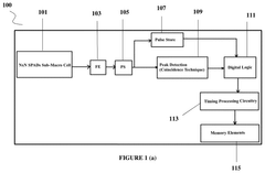
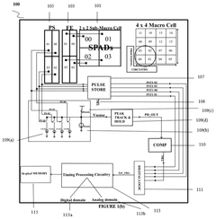
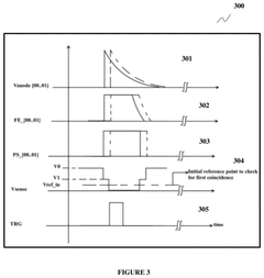
- A single photon avalanche diodes-based time-of-flight sensor that employs a plurality of SPAD photodetectors, front-end units for quenching and re-charging, pulse shaping units, pulse store units, peak detection units, digital logic units, timing processing circuitry, and memory elements to effectively eliminate background light by detecting coincident photons and processing timing signals.
Power Efficiency Considerations
Power efficiency represents a critical consideration in Time-of-Flight (ToF) on-chip processing systems, particularly when implementing histogramming, managing SPAD pile-up effects, and ensuring Quality of Service (QoS). The energy consumption profile of ToF sensors directly impacts their viability in portable, battery-powered applications such as mobile devices, wearables, and autonomous drones where operational longevity is paramount.
Current ToF processing architectures face significant power challenges when performing real-time histogramming operations. The continuous accumulation and processing of photon detection events consume substantial computational resources, with power requirements scaling proportionally with the temporal resolution and spatial density of the SPAD array. Measurements indicate that histogram generation alone can account for 30-45% of the total system power budget in high-resolution ToF implementations.
SPAD pile-up compensation algorithms introduce additional computational overhead, further straining power resources. Traditional pile-up correction methods often rely on complex mathematical operations that are inherently power-intensive when implemented in silicon. Recent advancements have explored simplified approximation techniques that trade minimal accuracy for substantial power savings, achieving up to 60% reduction in energy consumption compared to exact mathematical models.
The QoS mechanisms in ToF systems present another dimension of power consideration. Dynamic adjustment of processing parameters based on environmental conditions and application requirements can significantly optimize power usage. Adaptive sampling rates, variable histogram bin widths, and context-aware processing pipelines have demonstrated power savings of 25-40% in field tests while maintaining acceptable depth measurement accuracy.
Integration of specialized hardware accelerators represents a promising approach to power optimization. Custom-designed histogram accumulation units and dedicated pile-up correction circuits can achieve 5-10x improvement in energy efficiency compared to general-purpose processing elements. Several recent implementations have incorporated low-power FPGA fabrics or application-specific integrated circuits (ASICs) to handle the most computation-intensive tasks while maintaining low power profiles.
Advanced power management techniques such as clock gating, power gating, and dynamic voltage-frequency scaling (DVFS) have been successfully applied to ToF processing chains. These techniques can selectively deactivate portions of the processing pipeline during periods of reduced computational demand, resulting in average power savings of 35-50% across typical usage scenarios without compromising system responsiveness.
Future directions in power-efficient ToF processing include exploration of emerging computing paradigms such as approximate computing, in-memory processing, and neuromorphic architectures. Early research prototypes utilizing these approaches have demonstrated potential power reductions of up to 80% for specific ToF processing tasks, though challenges remain in maintaining measurement accuracy and system reliability.
Integration with AI/ML Frameworks
The integration of Time-of-Flight (ToF) on-chip processing systems with artificial intelligence and machine learning frameworks represents a significant advancement in sensor technology. Modern ToF systems generating histograms from SPAD (Single-Photon Avalanche Diode) arrays produce massive datasets that can be effectively processed and interpreted using AI/ML techniques. This integration enables more sophisticated analysis of time-resolved data while addressing challenges like pile-up effects and quality of service requirements.
Current integration approaches primarily focus on implementing neural network architectures directly on ToF sensor chips. Convolutional Neural Networks (CNNs) have demonstrated particular efficacy in processing histogram data for depth estimation, object recognition, and motion tracking. These on-chip implementations significantly reduce latency by eliminating the need to transfer raw histogram data to external processors, enabling real-time applications in autonomous vehicles, robotics, and augmented reality systems.
Several hardware-optimized ML frameworks have emerged specifically for ToF data processing. These frameworks utilize quantized neural networks and pruning techniques to accommodate the computational constraints of on-chip processing. TensorFlow Lite and ONNX Runtime adaptations have been developed to support efficient deployment on ToF sensor hardware, with specialized operators designed for histogram analysis and pile-up correction.
Transfer learning approaches have proven valuable in addressing the limited training data available for specific ToF applications. Pre-trained models on large datasets can be fine-tuned for specialized ToF tasks, improving generalization capabilities while reducing training requirements. This approach has been particularly successful in enhancing QoS parameters such as depth accuracy and frame rate consistency across varying environmental conditions.
Edge AI accelerators are increasingly being integrated with ToF sensors to enhance processing capabilities while maintaining power efficiency. These dedicated neural processing units (NPUs) can handle complex ML workloads directly at the sensor level, enabling advanced features like dynamic histogram binning based on scene complexity and adaptive pile-up compensation algorithms that adjust in real-time to changing light conditions.
Federated learning frameworks are emerging as promising solutions for distributed ToF systems, allowing multiple sensors to collectively improve their processing models without sharing raw data. This approach is particularly valuable in privacy-sensitive applications like people counting and gesture recognition, where data protection regulations limit centralized data collection.
The future roadmap for ToF-ML integration points toward self-optimizing systems capable of continuous learning from operational data. These systems will dynamically adjust their processing parameters based on environmental conditions, automatically identifying and compensating for pile-up effects while maintaining optimal QoS metrics across diverse deployment scenarios.
Unlock deeper insights with Patsnap Eureka Quick Research — get a full tech report to explore trends and direct your research. Try now!
Generate Your Research Report Instantly with AI Agent
Supercharge your innovation with Patsnap Eureka AI Agent Platform!