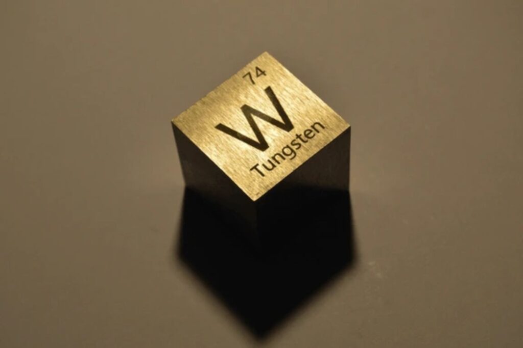
Tungsten, also known as wolfram, is a dense, heat-resistant metal valued for its exceptional mechanical strength, high melting point (3422 °C), and conductivity. As industries evolve toward demanding operational environments and miniaturized high-efficiency systems, tungsten’s unique properties make it indispensable across electronics, aerospace, medical imaging, and more.
From radiation shielding in healthcare to high-performance coatings in military tools, tungsten’s versatility enables both legacy and emerging applications. This article explores tungsten’s key properties, application domains, competitive advantages, limitations, and future directions—amplified through PatSnap Eureka AI Agent.

Material Composition & Key Properties
- Atomic Number: 74
- Melting Point: 3422 °C – highest of all metals
- Density: 19.3 g/cm³
- Crystal Structure: Body-Centered Cubic (BCC)
- Hardness: ~7.5 Mohs
- Electrical Conductivity: High (but lower than Cu/Ag)
- Thermal Conductivity: ~173 W/m·K
- Oxidation Resistance: Moderate (improves with alloying or coatings)
Preparation Methods:
- Hydrogen reduction of tungsten oxides
- Powder metallurgy (pressing + sintering)
- Plasma spheroidization for 3D printing
- Recycling from hard metal scrap
Certainly! Below is the Application Domains section written according to your structure and using the classified report titles. Each domain includes: background, material mechanism, research trends, and linked reports (minimum 7 per domain), written in English with clear, cohesive transitions.
Application Domains
Advanced Manufacturing & Processing
As advanced manufacturing evolves, industries demand materials that can maintain structural integrity under extreme thermal and mechanical loads. The growing complexity of components in aerospace, electronics, and defense sectors calls for precise control over material microstructure and consistency during mass production. Tungsten’s high melting point, density, and machinability make it an ideal candidate for powder metallurgy, sintering, and additive manufacturing processes.
Tungsten empowers next-generation processing by enabling ultra-fine powders, dense sintered parts, and advanced coating systems. Its ability to be alloyed, recycled, and finely controlled at the microstructural level allows manufacturers to meet precision and durability requirements while reducing material waste.
Recent research is focused on improving tungsten’s processability through powder refinement, recycling pathways, and advanced shaping techniques like plasma spheroidization. Industrial efforts are converging around cost reduction and sustainability through circular processing strategies.
Related Reports:
- How Is Tungsten Made?
- How To Optimize Tungsten Alloys For Durability?
- How To Achieve Ultra-Fine Tungsten Particles?
- How To Improve Tungsten Filament Manufacturing?
- How To Improve Tungsten’s Machinability?
- How To Streamline Tungsten Recovery Techniques?
- How To Reduce Manufacturing Costs For Tungsten Products?
- How To Increase Efficiency Of Tungsten Powders?
Electronics & Semiconductors
With the scaling of microelectronics, materials used in semiconductors and circuitry must withstand high thermal loads while ensuring reliable conductivity. Traditional materials such as copper or aluminum often fall short in extreme-temperature or miniaturized environments. Tungsten’s thermal stability and electromigration resistance have made it a go-to material for gate electrodes, interconnects, and heat sinks.
Tungsten enables compact, heat-tolerant electronic systems by providing both structural support and electrical performance. Its low thermal expansion and compatibility with silicon substrates make it suitable for advanced device architectures, from high-energy computing chips to photonic interposers.
The electronics industry is increasingly exploring tungsten for use in AI hardware, optoelectronics, and quantum computing platforms. Researchers are developing tungsten-based nanowires, transparent conductors, and sputtering targets to support future miniaturization and functionality.
Related Reports:
- Tungsten’s Role In High-Temperature Electronics
- Tungsten Breakthroughs In Artificial Intelligence Hardware
- New Frontiers In Tungsten Semiconductor Technology
- Tungsten’s Role In Next-Gen Photonic Devices
- How To Maximize Tungsten Conductivity In Circuits?
- Tungsten In The Realm Of High-Energy Physics
- How To Utilize Tungsten For Optoelectronic Advancements?
Energy, Aerospace & Nuclear
Energy systems and aerospace platforms demand materials that can survive extreme environments, including radiation, thermal cycling, and high-velocity impacts. As space exploration intensifies and fusion energy emerges as a priority, tungsten’s durability and resistance to neutron damage become crucial.
Tungsten plays a pivotal role in advanced propulsion systems, fusion reactor walls, and high-efficiency energy storage. It maintains structural integrity under rapid heating and prolonged exposure to radiation—conditions typical in spacecraft and nuclear systems.
Current research centers on tungsten-based plasma-facing materials for ITER fusion reactors, heat-resistant components in space vehicles, and radiation-shielding alloys for energy grids. Industry leaders are also examining tungsten composites for reducing weight while preserving thermal performance.
Related Reports:
- Exploring Tungsten’s Potential In Fusion Reactors
- Tungsten Alloys In Nuclear Reactor Safety
- Exploring Tungsten’s Role In Space Exploration
- Future Of Tungsten In Aerospace Applications
- Tungsten’s Impact On Energy Storage Systems
- Tungsten And The Progress In Inertial Confinement Fusion
- Advancing Energy Efficiency With Tungsten Technologies
Wear Resistance, Tools & Coatings
Mechanical systems in defense, mining, and heavy manufacturing require surfaces that can resist wear, corrosion, and thermal degradation. Traditional alloys and ceramics often erode quickly under friction or extreme temperature cycling. Tungsten, especially in carbide and alloyed forms, offers exceptional protection in such conditions.
By forming dense, adherent coatings or being incorporated into cutting tools and hardfacing layers, tungsten significantly extends the operational life of mechanical components. It minimizes tool wear, reduces downtime, and ensures dimensional accuracy in high-stress operations.
Ongoing innovation focuses on tungsten-carbide composites, vapor-deposited tungsten coatings, and wear-resistant nanostructured films. Researchers aim to combine extreme durability with easier machinability and lower material costs.
Related Reports:
- Tungsten Innovations: Reducing Wear In Devices
- How To Improve Tungsten’s Corrosion Resistance?
- Exploring Tungsten Carbide’s Industrial Applications
- Tungsten Coatings: Protecting Against Extreme Conditions
- Tungsten And Its Role In High-Performance Tools
- Tungsten: Critical Material In Hardfacing Alloys
- Tungsten In The Evolution Of Wear-Resistant Materials
- Tungsten And The Development Of Wear-Resistant Coatings
Medical & Imaging Technologies
Medical imaging and therapeutic systems require materials that provide effective radiation shielding and precise mechanical performance. Lead-based materials are toxic and environmentally problematic, prompting a shift toward safer alternatives. Tungsten offers high X-ray attenuation, excellent biocompatibility, and mechanical precision, making it ideal for surgical instruments and imaging components.
Tungsten is used in collimators, shielding housings, and diagnostic tools for CT, PET, and linear accelerator systems. It also supports the fabrication of fine surgical tips and dental tools where both rigidity and non-toxicity are required.
Research efforts are expanding tungsten’s use in polymer blends, biomedical composites, and even biodegradable forms for temporary implants. The focus is on increasing performance while minimizing environmental and biological risk.
Related Reports:
- Tungsten’s Impact On Medical Imaging Technology
- How To Utilize Tungsten For Radiation Shielding?
- Tungsten’s Application In Advanced Medical Tooling
- How To Integrate Tungsten In Biocompatible Applications?
- How To Refine Tungsten-Polymer Blends?
- Tungsten As A Catalyst For Industrial Transformation
- How To Innovate With Tungsten For Biocompatible Applications?
Sustainability, Innovation & Future Technologies
As sustainability becomes a global imperative, materials must not only perform well but also be recyclable, low-impact, and adaptable to emerging technologies. Tungsten, traditionally known for its durability, is now being reimagined through the lens of green innovation and smart material integration.
Tungsten contributes to a circular economy by enabling high-value recycling, eco-friendly extraction, and long-lifetime products. Its compatibility with nanotechnology and additive manufacturing opens new doors for flexible, miniaturized, and intelligent devices.
Research is pushing the frontiers in tungsten-based nanowires, transparent conductors, smart coatings, and 3D-printable formulations. These advancements are driving change in electronics, IoT, and wearables while reducing environmental burden.
Related Reports:
- Tungsten In 3D Printing: A New Frontier
- How To Boost Tungsten Recycling Processes?
- Tungsten Nanocomposites: Next-Gen Material Science
- Tungsten As A Sustainable Resource In Manufacturing
- How To Reduce Tungsten’s Environmental Impact?
- Tungsten’s Contribution To Smart Material Development
- Innovative Uses Of Tungsten Nanowires In Electronics
- Tungsten And Emerging Trends In Magnet Technology
Comparative Advantages & Limitations
| Feature | Advantage ✅ | Limitation |
|---|---|---|
| Melting Point | Extremely high (3422 °C) | Processing challenges |
| Density | High – ideal for shielding | Adds weight to devices |
| Electrical & Thermal Conductivity | Good under heat stress | Less conductive than Cu/Ag |
| Wear Resistance | Excellent (esp. in carbide form) | Brittle without alloying or blending |
| Radiation Shielding | Effective | Expensive in large-scale applications |
| Biocompatibility | High | Needs surface treatment in implants |
Future Outlook & Research Frontiers
Tungsten research is pivoting toward nanoengineering, additive manufacturing, and sustainability:
- AI-Designed Alloys for optimized fatigue and corrosion performance
- Tungsten Composites with polymers or ceramics for weight savings
- Fusion-Ready Materials enabling long-term plasma interactions
- Eco-Friendly Extraction using bioleaching or low-impact chemistry
- Tungsten-Coated Sensors in next-gen medical or quantum devices
Conclusion & Key Takeaways
Tungsten stands as a pillar of material innovation—balancing thermal resilience, mechanical strength, and multifunctional integration. Its role in electronics, aerospace, defense, and medical sectors continues to evolve, promising even greater value as global industries shift toward sustainability and miniaturization.
Now is the perfect time to explore how tungsten can transform your material strategies.
Accelerate Innovation with PatSnap Eureka AI Agent
Tungsten’s innovation landscape is vast—and complex. PatSnap Eureka AI Agent helps researchers, engineers, and business leaders uncover trends, benchmark technologies, and identify innovation white spaces.
👉 Request a free Eureka demo today to explore how your team can stay ahead in tungsten research and beyond.