Innovative Uses Of Tungsten Nanowires In Electronics
Tungsten Nanowire Evolution and Objectives
Tungsten nanowires have emerged as a promising material in the field of electronics, with a rich history of development and ambitious objectives for future applications. The evolution of tungsten nanowire technology can be traced back to the early 2000s when researchers first began exploring the potential of nanoscale tungsten structures. Initially, the focus was on developing reliable synthesis methods to produce high-quality tungsten nanowires with controlled dimensions and properties.
As the fabrication techniques improved, researchers started to investigate the unique properties of tungsten nanowires, such as their high melting point, excellent mechanical strength, and superior electrical conductivity. These characteristics made them attractive candidates for various electronic applications, particularly in areas where traditional materials faced limitations.
The objectives for tungsten nanowire research and development have evolved significantly over time. In the early stages, the primary goal was to achieve consistent and scalable production of nanowires with uniform properties. This was crucial for enabling further research and potential commercialization. As synthesis methods matured, the focus shifted towards understanding and optimizing the electronic properties of tungsten nanowires at the nanoscale.
One of the key objectives in recent years has been to integrate tungsten nanowires into functional electronic devices. This includes exploring their potential as interconnects in nanoelectronics, where their high conductivity and resistance to electromigration make them promising alternatives to conventional copper interconnects. Researchers have also been investigating the use of tungsten nanowires in field emission devices, leveraging their high aspect ratio and excellent electron emission properties.
Another important objective has been to explore the potential of tungsten nanowires in energy-related applications. This includes their use in thermoelectric devices, where the nanowire structure can enhance phonon scattering and improve thermoelectric efficiency. Additionally, researchers have been investigating tungsten nanowires as components in advanced solar cells and energy storage devices.
The current objectives for tungsten nanowire technology are multifaceted and ambitious. There is a strong focus on developing novel fabrication techniques that can produce nanowires with even more precise control over their structure and properties. This includes exploring methods for creating complex nanowire architectures and heterostructures that combine tungsten with other materials to achieve enhanced functionality.
Furthermore, researchers are aiming to push the boundaries of tungsten nanowire applications in electronics. This involves developing innovative device concepts that can fully exploit the unique properties of these nanomaterials. For instance, there is growing interest in using tungsten nanowires in quantum computing applications, where their robust nature and potential for precise manipulation make them attractive candidates for creating stable qubit structures.
Electronic Market Demand Analysis
The electronic market has shown a growing demand for innovative materials that can enhance the performance and capabilities of various devices. Tungsten nanowires have emerged as a promising candidate in this regard, with potential applications across multiple segments of the electronics industry.
In the semiconductor sector, there is a significant interest in using tungsten nanowires as interconnects in integrated circuits. As device dimensions continue to shrink, traditional copper interconnects face challenges related to increased resistance and electromigration. Tungsten nanowires offer superior electrical conductivity and thermal stability, making them attractive for next-generation chip designs. Market analysts project that the global semiconductor interconnect market will reach $10 billion by 2025, with advanced materials like tungsten nanowires poised to capture a growing share.
The display technology market is another area where tungsten nanowires are gaining traction. These nanowires can be used to create transparent conductive films, which are essential components in touchscreens, OLED displays, and flexible electronics. The global transparent conductive film market is expected to exceed $8 billion by 2026, driven by the increasing adoption of smartphones, tablets, and wearable devices. Tungsten nanowires offer advantages over traditional materials like indium tin oxide (ITO), including better flexibility and lower production costs.
In the energy storage sector, tungsten nanowires are being explored for use in advanced battery technologies. Their high surface area and excellent electrical conductivity make them suitable for electrode materials in lithium-ion batteries and supercapacitors. The global energy storage market is projected to grow at a CAGR of 20% from 2021 to 2026, reaching a value of $19 billion. Innovations in electrode materials, including tungsten nanowires, are expected to play a crucial role in meeting the increasing demand for high-performance energy storage solutions.
The aerospace and defense electronics market is also showing interest in tungsten nanowires for their potential in developing robust and lightweight components. These nanowires can be used in sensors, actuators, and electromagnetic shielding applications. The global aerospace and defense electronics market is forecasted to reach $200 billion by 2025, with a growing emphasis on advanced materials for next-generation systems.
While the market potential for tungsten nanowires in electronics is significant, challenges remain in scaling up production and integrating these materials into existing manufacturing processes. However, as research and development efforts continue, and as electronic device manufacturers seek innovative solutions to meet evolving consumer demands, the adoption of tungsten nanowires is expected to accelerate across various electronic market segments.
Tungsten Nanowire Tech Status and Challenges
Tungsten nanowires have emerged as a promising material in the field of electronics, offering unique properties that could revolutionize various applications. However, the current state of tungsten nanowire technology faces several challenges that need to be addressed for widespread adoption.
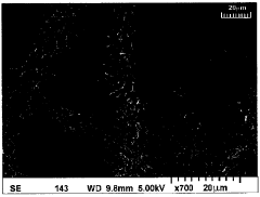
The development of tungsten nanowires has made significant progress in recent years, with researchers successfully synthesizing these structures with diameters as small as a few nanometers. The primary methods for fabrication include chemical vapor deposition, electrochemical deposition, and template-assisted growth. These techniques have enabled the production of high-quality nanowires with controlled dimensions and properties.
One of the main advantages of tungsten nanowires is their exceptional mechanical strength and thermal stability. These properties make them ideal for use in high-temperature and high-stress environments, such as in advanced microelectronics and aerospace applications. Additionally, tungsten nanowires exhibit excellent electrical conductivity, which is crucial for their integration into electronic devices.
Despite these promising characteristics, several challenges hinder the widespread adoption of tungsten nanowires in electronics. One significant obstacle is the difficulty in achieving uniform and reproducible growth of nanowires with consistent properties. The synthesis process is highly sensitive to environmental conditions, making it challenging to scale up production for commercial applications.
Another major challenge is the integration of tungsten nanowires into existing electronic manufacturing processes. The high melting point of tungsten (3422°C) makes it difficult to manipulate and incorporate these nanowires into conventional semiconductor fabrication techniques. This incompatibility necessitates the development of new manufacturing methods and equipment specifically tailored for tungsten nanowire-based devices.
The potential for oxidation is another concern in tungsten nanowire technology. When exposed to air, tungsten nanowires can form an oxide layer, which may alter their electrical and mechanical properties. This oxidation issue requires the development of effective passivation techniques or protective coatings to maintain the nanowires' performance over time.
Furthermore, the characterization and testing of tungsten nanowire-based devices present unique challenges. Traditional testing methods may not be suitable for evaluating the performance of these nanoscale structures, necessitating the development of new measurement techniques and standards.
From a geographical perspective, research on tungsten nanowires is distributed across various regions, with notable contributions from North America, Europe, and Asia. Leading research institutions and companies in these areas are actively working to overcome the current limitations and unlock the full potential of tungsten nanowires in electronics.
In conclusion, while tungsten nanowires show great promise for innovative electronic applications, significant technological hurdles must be overcome. Addressing these challenges will require collaborative efforts from researchers, engineers, and manufacturers to develop new fabrication techniques, integration methods, and characterization tools. As these obstacles are surmounted, tungsten nanowires are poised to play a crucial role in the next generation of electronic devices.
Current Tungsten Nanowire Applications
01 Synthesis methods for tungsten nanowires
Various techniques are employed to synthesize tungsten nanowires, including chemical vapor deposition, electrodeposition, and template-assisted growth. These methods allow for the controlled production of nanowires with specific dimensions and properties, enabling their use in diverse applications.- Synthesis methods for tungsten nanowires: Various techniques are employed to synthesize tungsten nanowires, including chemical vapor deposition, electrodeposition, and template-assisted growth. These methods allow for the controlled production of nanowires with specific dimensions and properties, enabling their use in diverse applications.
- Applications in electronic devices: Tungsten nanowires are utilized in electronic devices due to their excellent electrical conductivity and high melting point. They are incorporated into field-effect transistors, memory devices, and interconnects, enhancing performance and miniaturization of electronic components.
- Use in energy storage and conversion: Tungsten nanowires play a role in energy-related applications, such as electrodes for batteries and supercapacitors, as well as catalysts for fuel cells. Their high surface area and unique properties contribute to improved energy storage capacity and conversion efficiency.
- Sensing and detection applications: The unique properties of tungsten nanowires make them suitable for various sensing applications. They are used in gas sensors, biosensors, and chemical detectors, offering high sensitivity and rapid response times due to their large surface-to-volume ratio.
- Integration with other nanomaterials: Tungsten nanowires are often combined with other nanomaterials to create hybrid structures with enhanced properties. These composites find applications in areas such as photovoltaics, thermoelectrics, and reinforced materials, leveraging the unique characteristics of both tungsten and the complementary nanomaterials.
02 Applications in electronic devices
Tungsten nanowires are utilized in electronic devices such as field-effect transistors, memory devices, and sensors. Their unique electrical properties and high aspect ratio make them suitable for improving device performance and miniaturization in nanoelectronics.Expand Specific Solutions03 Integration with other nanomaterials
Tungsten nanowires are often combined with other nanomaterials to create hybrid structures or composites. These combinations can enhance the properties of the resulting materials, leading to improved performance in various applications such as energy storage and catalysis.Expand Specific Solutions04 Characterization and analysis techniques
Advanced characterization methods are employed to analyze the structure, composition, and properties of tungsten nanowires. These techniques include electron microscopy, spectroscopy, and electrical measurements, which are crucial for understanding and optimizing nanowire performance.Expand Specific Solutions05 Surface modification and functionalization
The surface of tungsten nanowires can be modified or functionalized to enhance their properties or enable specific applications. This includes coating with other materials, attaching functional groups, or creating core-shell structures to tailor the nanowires for use in areas such as catalysis, sensing, or biomedical applications.Expand Specific Solutions
Key Players in Nanowire Electronics
The innovative use of tungsten nanowires in electronics is an emerging field in the early stages of development. The market size is growing but still relatively small, with potential for significant expansion as applications in nanoelectronics and energy storage become more prevalent. Technologically, it's in a transitional phase from research to early commercialization. Companies like Samsung Electronics, Intel Corp., and IBM are at the forefront, leveraging their R&D capabilities to explore practical applications. Academic institutions such as Harvard College and Zhejiang University are contributing fundamental research. The involvement of diverse players, from established tech giants to specialized firms like Nanosys, Inc., indicates a competitive landscape with opportunities for breakthrough innovations.
Nanosys, Inc.
Samsung Electronics Co., Ltd.
Core Innovations in Nanowire Integration
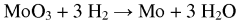
- A process involving the dissolution of technical grade molybdenum trioxide in aqueous ammonium hydroxide with the addition of metal generating compounds like calcium, iron, and manganese to precipitate tungsten, allowing for selective separation and purification.
- The synthesis of one-dimensional metal and metal oxide nanostructures with varied shapes such as wires, rods, needles, and flowers is achieved through chemical vapor deposition, where the oxygen content and doping elements like sulfur or carbon are controlled to produce non-stoichiometric compositions and composite structures, allowing for tunable properties and morphologies.
Environmental Impact Assessment
The integration of tungsten nanowires in electronics presents both opportunities and challenges from an environmental perspective. These nanomaterials offer potential improvements in device performance and efficiency, which could lead to reduced energy consumption and longer-lasting electronic products. However, their production, use, and disposal also raise concerns about potential environmental impacts.
The manufacturing process of tungsten nanowires typically involves energy-intensive methods and the use of potentially hazardous chemicals. This could contribute to increased carbon emissions and chemical waste if not properly managed. However, advancements in green synthesis techniques are being explored to mitigate these issues, such as using environmentally friendly reducing agents and optimizing production processes to minimize waste.
During the use phase, tungsten nanowires in electronics may contribute to improved energy efficiency and device longevity. This could result in a net positive environmental impact by reducing the overall energy consumption of electronic devices and potentially decreasing the frequency of device replacement. The enhanced thermal and electrical properties of tungsten nanowires could lead to more efficient heat dissipation and power management in electronic components, further contributing to energy savings.
End-of-life considerations for electronics containing tungsten nanowires are crucial. The small size and unique properties of nanomaterials can make them challenging to recycle or dispose of safely. There are concerns about the potential release of nanoparticles into the environment during the disposal or recycling process, which could have unforeseen ecological consequences. Research is ongoing to develop effective methods for recovering and recycling nanomaterials from electronic waste.
The potential for bioaccumulation and toxicity of tungsten nanowires in the environment is an area of active study. While bulk tungsten is generally considered to have low toxicity, the unique properties of nanoscale materials may lead to different environmental behaviors and interactions with living organisms. Long-term studies are needed to fully understand the potential ecological impacts of these materials if released into the environment.
Regulatory frameworks and industry standards are evolving to address the environmental implications of nanomaterials in electronics. This includes the development of guidelines for safe handling, use, and disposal of nano-enabled electronic products. As the use of tungsten nanowires in electronics expands, it will be crucial to continue monitoring their environmental impact and refining best practices for sustainable implementation throughout the product lifecycle.
Nanowire Manufacturing Processes
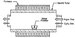
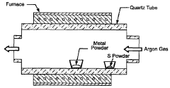
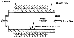
The manufacturing processes for tungsten nanowires have evolved significantly, leveraging advanced techniques to produce high-quality nanostructures suitable for innovative electronic applications. One of the primary methods employed is chemical vapor deposition (CVD), which allows for precise control over nanowire growth parameters. In this process, tungsten-containing precursor gases are introduced into a reaction chamber, where they decompose and deposit onto a substrate, forming nanowires with controlled dimensions and crystalline structure.
Another widely used technique is electrochemical deposition, which offers advantages in terms of scalability and cost-effectiveness. This method involves the reduction of tungsten ions from an electrolyte solution onto a conductive substrate, resulting in the formation of nanowires. By carefully controlling parameters such as current density, electrolyte composition, and deposition time, researchers can tailor the properties of the resulting nanowires to meet specific requirements for electronic applications.
Template-assisted synthesis has also gained prominence in tungsten nanowire manufacturing. This approach utilizes pre-existing nanostructured templates, such as anodic aluminum oxide (AAO) membranes, to guide the growth of nanowires. The template pores act as nanoscale reactors, confining the growth process and enabling the production of highly uniform and aligned nanowire arrays. This method is particularly advantageous for applications requiring precise spatial arrangement of nanowires.
Recent advancements in manufacturing processes have focused on enhancing the control over nanowire morphology and composition. Vapor-liquid-solid (VLS) growth, for instance, has been adapted for tungsten nanowire synthesis, allowing for the production of single-crystalline structures with improved electronic properties. This method involves the use of metal catalyst particles to facilitate nanowire growth, resulting in highly oriented and defect-free nanostructures.
Post-synthesis treatments play a crucial role in optimizing the performance of tungsten nanowires for electronic applications. Thermal annealing processes are commonly employed to improve crystallinity, reduce defects, and enhance electrical conductivity. Additionally, surface functionalization techniques have been developed to modify the chemical and physical properties of nanowire surfaces, enabling better integration with other materials and improved performance in specific electronic devices.
As the demand for miniaturized and high-performance electronic components continues to grow, researchers are exploring novel manufacturing approaches to further enhance the properties and scalability of tungsten nanowire production. These efforts include the development of continuous flow synthesis methods for large-scale production, as well as the integration of in-situ characterization techniques to enable real-time monitoring and control of nanowire growth processes.