How To Foster Innovative Tungsten Sensor Technologies?
Tungsten Sensor Evolution and Objectives
Tungsten sensors have undergone significant evolution since their inception, driven by the increasing demand for high-performance sensing technologies in extreme environments. The journey of tungsten sensor development can be traced back to the early 20th century when the unique properties of tungsten, such as its high melting point and excellent thermal conductivity, were first recognized for sensing applications.
Initially, tungsten sensors were primarily used in temperature measurement for industrial processes. As technology advanced, the potential of tungsten in various sensing applications became apparent. The 1960s and 1970s saw a surge in research and development, focusing on improving the sensitivity, accuracy, and durability of tungsten-based sensors. This period marked the transition from simple temperature sensors to more sophisticated devices capable of measuring pressure, strain, and other physical parameters.
The advent of microelectronics and nanotechnology in the late 20th and early 21st centuries opened new avenues for tungsten sensor innovation. Researchers began exploring ways to integrate tungsten into micro-electromechanical systems (MEMS) and nanostructures, leading to the development of highly sensitive and miniaturized sensors. These advancements enabled the application of tungsten sensors in previously inaccessible environments and industries.
Today, the objectives of tungsten sensor technology are multifaceted and ambitious. One primary goal is to enhance the performance of sensors in extreme conditions, such as high-temperature environments in aerospace and automotive industries. Researchers are striving to develop tungsten sensors that can maintain accuracy and reliability at temperatures exceeding 2000°C, pushing the boundaries of material science and sensor design.
Another critical objective is the miniaturization of tungsten sensors without compromising their performance. This aim aligns with the growing trend of IoT devices and wearable technologies, where compact yet highly efficient sensors are in high demand. Achieving this goal requires innovative approaches in material processing, sensor architecture, and signal processing techniques.
Improving the multifunctionality of tungsten sensors is also a key focus. Scientists and engineers are working on developing sensors that can simultaneously measure multiple parameters, such as temperature, pressure, and chemical composition. This multifunctionality would significantly enhance the utility of tungsten sensors in complex systems and reduce the overall number of sensors required in various applications.
Lastly, there is a growing emphasis on developing eco-friendly and sustainable tungsten sensor technologies. This objective involves exploring ways to reduce the environmental impact of sensor production, improve energy efficiency, and enhance the recyclability of sensor components. As global awareness of environmental issues increases, the sustainability of tungsten sensor technologies becomes crucial for their long-term viability and acceptance in various industries.
Market Demand Analysis for Tungsten Sensors
The market demand for tungsten sensors has been experiencing significant growth, driven by the increasing need for high-performance sensing technologies across various industries. Tungsten's unique properties, including its high melting point, excellent thermal and electrical conductivity, and resistance to corrosion, make it an ideal material for sensor applications in extreme environments.
In the automotive sector, tungsten sensors are gaining traction for use in engine management systems, exhaust gas monitoring, and temperature control. As vehicle manufacturers strive to meet stringent emission standards and improve fuel efficiency, the demand for reliable and durable sensors capable of withstanding high temperatures and harsh conditions continues to rise.
The aerospace industry represents another key market for tungsten sensors. These sensors are crucial for monitoring engine performance, structural health, and environmental conditions in aircraft and spacecraft. With the growing emphasis on safety and efficiency in aviation, the demand for advanced sensing technologies is expected to fuel the market for tungsten sensors in this sector.
In the industrial sector, tungsten sensors find applications in process control, quality assurance, and safety monitoring systems. Industries such as metallurgy, chemical processing, and power generation require sensors that can operate reliably in high-temperature and corrosive environments, further driving the demand for tungsten-based sensing solutions.
The medical field is emerging as a promising market for tungsten sensors, particularly in diagnostic imaging equipment and radiation therapy devices. Tungsten's ability to shield against radiation while providing precise sensing capabilities makes it valuable in medical applications where accuracy and safety are paramount.
The global push towards Industry 4.0 and the Internet of Things (IoT) is also contributing to the increased demand for advanced sensing technologies. Tungsten sensors, with their robustness and reliability, are well-positioned to play a crucial role in smart manufacturing systems and connected industrial environments.
As environmental concerns grow, there is a rising demand for sensors capable of monitoring air and water quality, as well as detecting pollutants. Tungsten sensors, with their resistance to chemical corrosion and ability to operate in harsh conditions, are becoming increasingly important in environmental monitoring applications.
The market for tungsten sensors is expected to see continued growth in the coming years, driven by technological advancements, expanding applications, and the need for sensors that can perform reliably in extreme conditions. However, challenges such as the high cost of tungsten and the complexity of sensor manufacturing processes may impact market growth. Addressing these challenges through innovative manufacturing techniques and material optimization will be crucial for fostering the development of tungsten sensor technologies and meeting the evolving market demands.
Current Challenges in Tungsten Sensor Technology
Tungsten sensor technology, while promising, faces several significant challenges that hinder its widespread adoption and innovation. One of the primary obstacles is the extreme operating conditions these sensors must endure. Tungsten's high melting point makes it suitable for harsh environments, but it also complicates the manufacturing process and integration with other sensor components.
The development of reliable and durable electrical connections poses another major challenge. The high temperatures at which tungsten sensors operate can cause degradation of traditional connection materials, leading to sensor failure or inaccurate readings. Researchers are actively seeking novel materials and connection techniques to overcome this limitation.
Miniaturization of tungsten sensors presents a significant hurdle. As industries demand smaller and more compact sensing solutions, reducing the size of tungsten sensors while maintaining their performance and durability becomes increasingly difficult. This challenge is particularly evident in applications such as aerospace and automotive industries, where space and weight constraints are critical.
The cost-effectiveness of tungsten sensor production remains a concern. The complex manufacturing processes and specialized equipment required for tungsten sensor fabrication contribute to higher production costs compared to sensors made from more common materials. This economic factor limits the widespread adoption of tungsten sensors in various applications.
Achieving high sensitivity and accuracy across a wide temperature range is another ongoing challenge. While tungsten sensors excel in high-temperature environments, maintaining consistent performance across varying temperature conditions proves difficult. Researchers are exploring advanced calibration techniques and novel sensor designs to address this issue.
The development of multi-functional tungsten sensors that can measure multiple parameters simultaneously is a growing area of interest. However, integrating additional sensing capabilities without compromising the core temperature-sensing function of tungsten sensors presents significant technical challenges.
Lastly, the long-term stability and drift characteristics of tungsten sensors under extreme conditions require further improvement. Ensuring consistent and reliable performance over extended periods in harsh environments is crucial for many industrial applications. Addressing this challenge involves ongoing research into material science and sensor design optimization.
Existing Tungsten Sensor Solutions
01 Innovative tungsten sensor designs
Advancements in tungsten sensor designs focus on improving sensitivity, durability, and performance in various applications. These innovations may include novel structures, materials integration, or miniaturization techniques to enhance the capabilities of tungsten-based sensors.- Innovative tungsten sensor designs: Advancements in tungsten sensor designs focus on improving sensitivity, durability, and performance in various applications. These innovations may include novel structures, materials integration, or miniaturization techniques to enhance sensor capabilities.
- Data processing and analysis for tungsten sensors: Development of sophisticated algorithms and data processing techniques to enhance the accuracy and reliability of tungsten sensor readings. This includes machine learning approaches, signal processing, and real-time data analysis methods.
- Integration of tungsten sensors in IoT and smart systems: Incorporation of tungsten sensors into Internet of Things (IoT) ecosystems and smart systems for improved monitoring and control. This involves developing communication protocols, cloud integration, and remote sensing capabilities for tungsten-based sensors.
- Application-specific tungsten sensor innovations: Customization and optimization of tungsten sensors for specific industrial, medical, or environmental applications. This includes developing sensors tailored for extreme conditions, high-precision measurements, or specialized detection needs.
- Manufacturing and production innovations for tungsten sensors: Advancements in manufacturing processes and production techniques for tungsten sensors, focusing on improving efficiency, reducing costs, and enhancing sensor quality. This may include novel fabrication methods, quality control systems, or automation in sensor production.
02 Data processing and analysis for tungsten sensors
Development of sophisticated algorithms and data processing techniques to enhance the accuracy and reliability of tungsten sensor readings. This includes machine learning approaches, signal processing, and data fusion methods to extract meaningful information from sensor outputs.Expand Specific Solutions03 Integration of tungsten sensors in IoT and smart systems
Incorporation of tungsten sensors into Internet of Things (IoT) ecosystems and smart systems for real-time monitoring and control. This involves developing communication protocols, networking solutions, and cloud-based platforms to enable seamless data collection and analysis from tungsten sensors.Expand Specific Solutions04 Application-specific tungsten sensor innovations
Customization and optimization of tungsten sensors for specific industrial, medical, or environmental applications. This includes tailoring sensor properties, packaging, and interfacing to meet the unique requirements of different sectors such as automotive, aerospace, or healthcare.Expand Specific Solutions05 Manufacturing and fabrication techniques for tungsten sensors
Development of advanced manufacturing processes and fabrication techniques to produce high-quality, cost-effective tungsten sensors at scale. This may involve innovations in materials science, microfabrication, and quality control methods to improve sensor production efficiency and reliability.Expand Specific Solutions
Key Players in Tungsten Sensor Industry
The innovative tungsten sensor technology market is in its growth phase, with increasing demand across various industries. The market size is expanding rapidly due to the material's unique properties and versatility in sensor applications. Technologically, the field is advancing, with companies like Applied Materials, Inc., STMicroelectronics, Inc., and QUALCOMM, Inc. leading in research and development. These firms, along with academic institutions such as Central South University and Xiamen University, are pushing the boundaries of tungsten sensor capabilities. The competitive landscape is diverse, featuring both established semiconductor giants and specialized materials companies, indicating a dynamic and evolving market with significant potential for further innovation and growth.
Applied Materials, Inc.
STMicroelectronics, Inc.
Core Innovations in Tungsten Sensing
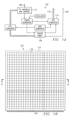
- A sensor element with a tungsten substrate having a specific electrical resistance and a surface relief with controlled irregularities, combined with a thin sensitive layer of platinum group metals, ensuring strong adhesion without chemical interaction, allowing for increased surface area and reduced energy consumption.
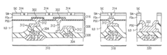
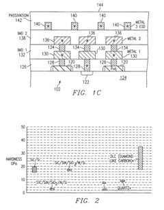
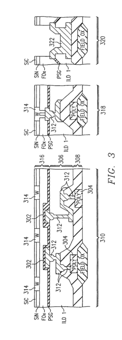
- Replacing aluminum metallization with a harder conductive material, such as tungsten, for all metallization levels, including contacts, vias, interconnects, capacitive electrodes, and electrostatic discharge protection lines, to enhance scratch resistance.
Materials Science Advancements for Tungsten Sensors
Recent advancements in materials science have significantly contributed to the development of innovative tungsten sensor technologies. The unique properties of tungsten, such as its high melting point, excellent thermal conductivity, and resistance to corrosion, make it an ideal material for sensor applications in extreme environments. However, traditional tungsten sensors often face limitations in terms of sensitivity, response time, and durability.
To address these challenges, researchers have been exploring novel approaches to enhance the performance of tungsten-based sensors. One promising direction is the development of nanostructured tungsten materials. By manipulating the material at the nanoscale, scientists have been able to create tungsten sensors with increased surface area and improved sensitivity. These nanostructured sensors exhibit faster response times and higher selectivity compared to their bulk counterparts.
Another significant advancement in tungsten sensor technology is the incorporation of composite materials. By combining tungsten with other elements or compounds, researchers have created sensors with enhanced properties. For example, tungsten-oxide composites have shown excellent gas sensing capabilities, particularly for detecting harmful gases in industrial environments. These composite materials offer improved stability and longer operational lifetimes compared to pure tungsten sensors.
Surface modification techniques have also played a crucial role in advancing tungsten sensor technologies. By tailoring the surface properties of tungsten sensors, researchers have been able to enhance their selectivity and sensitivity to specific target molecules. Techniques such as plasma treatment, chemical functionalization, and the deposition of catalytic layers have been employed to optimize sensor performance for various applications.
Furthermore, the integration of advanced manufacturing techniques has opened up new possibilities for tungsten sensor design. Additive manufacturing, or 3D printing, has enabled the fabrication of complex tungsten sensor structures with precise control over geometry and composition. This approach allows for the creation of sensors with optimized shapes and internal structures, leading to improved performance and functionality.
In recent years, there has been a growing interest in flexible and wearable tungsten sensors. By developing thin-film deposition techniques and exploring novel substrate materials, researchers have successfully created flexible tungsten-based sensors that can conform to curved surfaces. These advancements have paved the way for applications in wearable electronics, healthcare monitoring, and structural health monitoring of complex geometries.
Environmental Impact of Tungsten Sensor Production
The production of tungsten sensors has significant environmental implications that warrant careful consideration. The extraction and processing of tungsten, a key component in these sensors, can lead to substantial ecological disturbances. Mining operations often result in habitat destruction, soil erosion, and water pollution. The energy-intensive refining process contributes to greenhouse gas emissions, exacerbating climate change concerns.
Furthermore, the manufacturing of tungsten sensors involves the use of various chemicals and materials that may pose environmental risks if not properly managed. These include acids, solvents, and other potentially hazardous substances used in etching, cleaning, and coating processes. Proper disposal and treatment of these materials are crucial to prevent contamination of soil and water resources.
Water usage is another critical environmental factor in tungsten sensor production. The manufacturing process requires substantial amounts of water for cooling, cleaning, and processing, potentially straining local water supplies in areas of production. Implementing water recycling and conservation measures can help mitigate this impact.
The environmental footprint of tungsten sensor production extends to energy consumption as well. The high-temperature processes required for tungsten processing and sensor fabrication demand significant energy inputs, often derived from fossil fuel sources. Transitioning to renewable energy sources for manufacturing facilities could substantially reduce the carbon footprint of production.
Waste management presents another environmental challenge. The production process generates various forms of waste, including metal scraps, chemical byproducts, and packaging materials. Implementing effective recycling and waste reduction strategies is essential to minimize landfill contributions and resource depletion.
As the demand for tungsten sensors grows, particularly in emerging technologies like autonomous vehicles and advanced manufacturing, the cumulative environmental impact of their production is likely to increase. This underscores the importance of developing more sustainable manufacturing processes and exploring alternative materials that could offer similar performance with reduced environmental consequences.
Addressing these environmental concerns requires a multifaceted approach. This includes investing in cleaner extraction methods, adopting more efficient manufacturing processes, implementing rigorous waste management protocols, and exploring eco-friendly alternatives to traditional tungsten sensor designs. By prioritizing sustainability in the development and production of tungsten sensors, the industry can foster innovation while minimizing its ecological footprint.