Tungsten’s Role In Next-Gen Photonic Devices
Tungsten Photonics Evolution
The evolution of tungsten's role in photonic devices has been marked by significant technological advancements and a growing recognition of its unique properties. Initially, tungsten was primarily used in traditional electronic applications due to its high melting point and excellent electrical conductivity. However, as the field of photonics emerged and expanded, researchers began to explore tungsten's potential in optical and optoelectronic devices.
In the early stages of photonic device development, tungsten found limited applications, mainly as a heat sink or electrode material. Its high thermal conductivity made it an ideal candidate for managing heat dissipation in high-power optical components. As the demand for more efficient and compact photonic devices grew, engineers started to investigate tungsten's optical properties more closely.
A significant breakthrough came with the discovery of tungsten's plasmonic properties in the infrared and visible spectrum. This revelation opened up new possibilities for tungsten in nanophotonic applications. Researchers found that tungsten nanostructures could support surface plasmon resonances, enabling the manipulation of light at the nanoscale. This led to the development of tungsten-based plasmonic devices, including sensors, modulators, and waveguides.
The advent of metamaterials further propelled tungsten's importance in photonics. Scientists discovered that carefully designed tungsten nanostructures could exhibit extraordinary optical properties not found in natural materials. This led to the creation of tungsten-based metamaterials with applications in perfect absorbers, thermal emitters, and optical cloaking devices.
As the field of photonics continued to advance, tungsten's role expanded into quantum photonics. Researchers began exploring tungsten-based quantum emitters, leveraging its unique electronic structure to create single-photon sources and other quantum optical components. This development has positioned tungsten as a promising material for future quantum communication and computing technologies.
Recent years have seen a surge in interest in tungsten disulfide (WS2) and other tungsten-based two-dimensional materials. These atomically thin materials exhibit exceptional optical and electronic properties, making them ideal candidates for next-generation photonic devices. Tungsten disulfide, in particular, has shown great potential in areas such as light-emitting diodes, photodetectors, and ultrafast optical switches.
The ongoing miniaturization of photonic devices has further emphasized tungsten's importance. Its compatibility with existing semiconductor fabrication processes and its ability to withstand high temperatures make it an attractive material for integrated photonic circuits. Researchers are now exploring ways to combine tungsten with other materials to create hybrid photonic structures with enhanced functionality and performance.
Market Demand Analysis
The market demand for next-generation photonic devices incorporating tungsten is experiencing significant growth, driven by the increasing need for high-performance, energy-efficient optical components across various industries. Telecommunications, data centers, and advanced computing systems are at the forefront of this demand, seeking solutions that can handle the ever-expanding data traffic while minimizing power consumption and heat generation.
In the telecommunications sector, the rollout of 5G networks and the anticipated 6G technology are creating a surge in demand for photonic devices capable of ultra-fast data transmission and processing. Tungsten-based photonic components offer promising characteristics for these applications, including enhanced thermal stability and improved electrical conductivity, which are crucial for maintaining signal integrity in high-frequency operations.
Data centers, another key market driver, are constantly seeking ways to improve their energy efficiency and data processing capabilities. The integration of tungsten in photonic devices presents an opportunity to develop more compact and power-efficient optical interconnects, potentially revolutionizing data center architectures and reducing operational costs.
The emerging field of quantum computing also contributes to the market demand for advanced photonic devices. Tungsten's unique properties make it a candidate for developing quantum photonic circuits, which are essential for quantum information processing and communication. As research in quantum technologies progresses, the demand for specialized photonic components is expected to grow substantially.
Consumer electronics represent another significant market segment driving the demand for tungsten-based photonic devices. The trend towards miniaturization and increased functionality in smartphones, wearables, and augmented reality devices is pushing manufacturers to explore novel materials and technologies. Tungsten's potential to enable smaller, more efficient optical components aligns well with these industry requirements.
In the automotive industry, the development of autonomous vehicles and advanced driver assistance systems (ADAS) is creating a new market for high-performance sensors and LiDAR systems. Tungsten's role in enhancing the performance of photonic devices could contribute to more accurate and reliable sensing technologies, crucial for the safety and effectiveness of autonomous driving systems.
The medical and biotechnology sectors are also showing increasing interest in advanced photonic devices. From improved imaging technologies to novel biosensors, tungsten-based photonic components could enable more precise diagnostics and treatment methods. This market segment is expected to grow as healthcare continues to embrace cutting-edge technologies for patient care and research.
Tungsten Photonic Challenges
Tungsten's integration into next-generation photonic devices presents several significant challenges that researchers and engineers must overcome. One of the primary obstacles is the material's high melting point, which makes it difficult to process and incorporate into delicate photonic structures. This characteristic, while beneficial for certain applications, complicates the fabrication of nanoscale tungsten components essential for advanced photonic devices.
Another challenge lies in tungsten's optical properties. While it exhibits excellent thermal stability and electrical conductivity, its interaction with light at various wavelengths can be complex. Researchers must carefully engineer tungsten-based structures to achieve the desired optical responses, such as enhanced light absorption or emission at specific frequencies. This requires precise control over the material's surface properties and nanostructure.
The integration of tungsten with other materials commonly used in photonics, such as silicon or III-V semiconductors, poses additional challenges. Ensuring compatibility and minimizing interfacial defects between tungsten and these materials is crucial for maintaining device performance and reliability. Moreover, the potential for interdiffusion or unwanted chemical reactions at elevated temperatures must be carefully managed.
Tungsten's susceptibility to oxidation in ambient conditions presents another hurdle. When exposed to air, especially at high temperatures, tungsten forms oxide layers that can significantly alter its optical and electrical properties. Developing effective passivation techniques or protective coatings is essential to maintain the long-term stability and performance of tungsten-based photonic devices.
The scalability of tungsten-based photonic components for large-scale production is also a concern. Current fabrication methods may not be suitable for high-volume manufacturing, necessitating the development of new, cost-effective production techniques that maintain the precision required for photonic applications.
Lastly, the environmental impact and sustainability of tungsten extraction and processing must be addressed. As demand for tungsten in photonic devices increases, finding more environmentally friendly sourcing and production methods becomes crucial to ensure the long-term viability of tungsten-based photonic technologies.
Current Tungsten Solutions
01 Tungsten deposition and film formation
Various methods and techniques for depositing tungsten and forming tungsten films on substrates. This includes chemical vapor deposition (CVD), physical vapor deposition (PVD), and atomic layer deposition (ALD) processes. These techniques are used to create thin, uniform tungsten layers for applications in semiconductor manufacturing and other industries.- Tungsten deposition methods: Various methods for depositing tungsten on substrates, including chemical vapor deposition (CVD) and atomic layer deposition (ALD). These techniques are used to create thin films of tungsten for applications in semiconductor manufacturing and other industries.
- Tungsten etching processes: Techniques for selectively etching tungsten layers in semiconductor fabrication. These processes are crucial for creating precise patterns and structures in integrated circuits and other microelectronic devices.
- Tungsten-based alloys and composites: Development of tungsten alloys and composite materials with enhanced properties for various applications. These materials combine tungsten with other elements to improve characteristics such as strength, hardness, and thermal stability.
- Tungsten in electronic components: Use of tungsten in the manufacture of electronic components, including interconnects, vias, and electrodes. Tungsten's high melting point and good electrical conductivity make it suitable for these applications in advanced semiconductor devices.
- Tungsten surface treatment and modification: Methods for treating and modifying tungsten surfaces to enhance their properties or compatibility with other materials. These techniques can improve adhesion, reduce oxidation, or alter the surface characteristics of tungsten components.
02 Tungsten-based alloys and composites
Development of tungsten-based alloys and composite materials with enhanced properties. These materials combine tungsten with other elements or compounds to improve characteristics such as strength, hardness, and thermal stability. Applications include high-temperature components, radiation shielding, and wear-resistant parts.Expand Specific Solutions03 Tungsten in semiconductor devices
Use of tungsten in various semiconductor device structures and manufacturing processes. This includes tungsten interconnects, contact plugs, and barrier layers. Tungsten is utilized for its low resistivity, high melting point, and compatibility with silicon-based technologies.Expand Specific Solutions04 Tungsten-based lighting and electron emission
Applications of tungsten in lighting technologies and electron emission devices. This includes tungsten filaments for incandescent lamps, cathodes for electron tubes, and field emission sources. Tungsten's high melting point and low vapor pressure make it suitable for these applications.Expand Specific Solutions05 Tungsten recycling and resource management
Methods for recycling tungsten-containing materials and managing tungsten resources. This includes processes for recovering tungsten from scrap, spent catalysts, and other waste streams. Techniques for purifying and refining recycled tungsten are also developed to meet the growing demand for this valuable metal.Expand Specific Solutions
Key Industry Players
The development of tungsten's role in next-generation photonic devices is in its early stages, with significant potential for market growth. The industry is transitioning from research to early commercialization, driven by the increasing demand for advanced photonic technologies. While the market size is currently modest, it is expected to expand rapidly as applications in telecommunications, data centers, and quantum computing mature. The technology's maturity varies across different applications, with companies like Applied Materials, IBM, and Samsung Electronics leading in research and development. Universities and research institutions, such as the University of Science & Technology Beijing and Centre National de la Recherche Scientifique, are also contributing significantly to advancing the field. The competitive landscape is diverse, with both established semiconductor companies and specialized materials firms like Chongyi Zhangyuan Tungsten Co., Ltd. and Xiamen Honglu Tungsten Molybdenum Industry Co., Ltd. vying for market share.
Applied Materials, Inc.
International Business Machines Corp.
Tungsten Photonic Patents
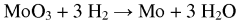
- A process involving the dissolution of technical grade molybdenum trioxide in aqueous ammonium hydroxide with the addition of metal generating compounds like calcium, iron, and manganese to precipitate tungsten, allowing for selective separation and purification.
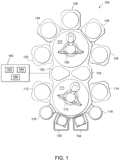
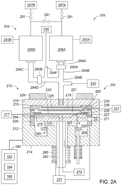
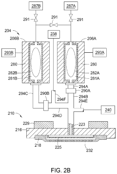
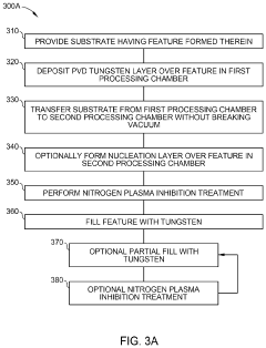
- A method involving physical vapor deposition (PVD) of a tungsten liner layer followed by exposure to nitrogen-containing radicals and tungsten-containing precursor gases in a single processing chamber without vacuum breaks, allowing for seamless tungsten fill layer formation with reduced resistivity and minimized defects.
Material Supply Chain
The tungsten supply chain plays a crucial role in the development and production of next-generation photonic devices. As a key material in these advanced technologies, tungsten's availability, quality, and cost significantly impact the industry's growth and innovation potential.
Tungsten is primarily sourced from mines in China, which accounts for over 80% of global production. This concentration of supply introduces potential risks and vulnerabilities to the photonics industry. Other significant producers include Vietnam, Russia, and Bolivia, though their combined output is considerably smaller than China's.
The extraction and processing of tungsten ore involve complex procedures, including mining, concentration, and refining. These processes require specialized equipment and expertise, which are concentrated in a few key regions. The limited number of processing facilities capable of producing high-purity tungsten suitable for photonic applications creates potential bottlenecks in the supply chain.
Recycling and recovery of tungsten from end-of-life products and manufacturing waste have become increasingly important in recent years. This secondary supply helps mitigate some of the risks associated with primary production and contributes to a more sustainable material ecosystem for the photonics industry.
The global demand for tungsten in photonic devices is expected to grow significantly in the coming years, driven by advancements in areas such as optical communications, sensing, and quantum technologies. This increasing demand may put pressure on existing supply chains and potentially lead to price volatility.
To address these challenges, several strategies are being explored by industry stakeholders. These include diversifying supply sources, investing in new mining and processing technologies, and developing alternative materials that can partially substitute tungsten in certain applications. Additionally, efforts are being made to improve the efficiency of tungsten use in manufacturing processes and to enhance recycling capabilities.
The photonics industry is also closely monitoring geopolitical factors that could affect the tungsten supply chain. Trade tensions, environmental regulations, and shifts in global economic power dynamics all have the potential to impact the availability and cost of this critical material.
As next-generation photonic devices continue to evolve, the importance of a robust and resilient tungsten supply chain becomes increasingly apparent. Industry leaders and policymakers are working together to develop strategies that ensure a stable and sustainable supply of this vital material, enabling continued innovation and growth in the photonics sector.
Environmental Considerations
The integration of tungsten in next-generation photonic devices brings forth significant environmental considerations that must be carefully addressed. Tungsten, while offering exceptional properties for photonic applications, poses potential environmental challenges throughout its lifecycle.
Mining and extraction processes for tungsten can have substantial environmental impacts. These activities often involve large-scale operations that may lead to habitat disruption, soil erosion, and water pollution. The energy-intensive nature of tungsten extraction also contributes to increased carbon emissions, raising concerns about its carbon footprint in the photonics industry.
During the manufacturing phase of photonic devices incorporating tungsten, careful attention must be paid to waste management and emissions control. Tungsten-containing byproducts and residues require proper handling and disposal to prevent contamination of soil and water resources. Additionally, the use of chemical processes in tungsten refinement and device fabrication necessitates stringent environmental safeguards.
The operational phase of tungsten-based photonic devices presents both opportunities and challenges from an environmental perspective. On one hand, these devices often offer improved energy efficiency compared to traditional alternatives, potentially reducing overall energy consumption and associated environmental impacts. However, the long-term stability and durability of tungsten in photonic applications must be ensured to minimize the need for frequent replacements and reduce electronic waste.
End-of-life considerations for tungsten-containing photonic devices are crucial. Recycling and recovery of tungsten from these devices can help conserve this valuable resource and reduce the environmental burden of primary production. However, the complex nature of photonic devices may present challenges in efficient recycling processes, requiring innovative approaches to material separation and recovery.
The potential for tungsten to leach into the environment from discarded devices also raises concerns about long-term ecological impacts. While tungsten is generally considered less toxic than some other heavy metals, its accumulation in ecosystems and potential effects on wildlife and human health warrant further investigation and monitoring.
To address these environmental considerations, the photonics industry must adopt a holistic approach to sustainability. This includes implementing cleaner production techniques, optimizing resource efficiency, and designing devices with end-of-life recycling in mind. Collaboration between researchers, manufacturers, and environmental experts is essential to develop best practices and technologies that minimize the environmental footprint of tungsten-based photonic devices throughout their lifecycle.