

How To Push Boundaries In Tungsten-Based Technologies?
Tungsten Tech Evolution
Tungsten-based technologies have undergone significant evolution since the metal's discovery in the late 17th century. Initially valued for its high melting point and durability, tungsten found early applications in incandescent light bulbs and electrical contacts. The 20th century saw a rapid expansion of tungsten's use, particularly in the development of high-speed steel alloys and hard metal composites.
The advent of powder metallurgy techniques in the mid-20th century marked a pivotal moment in tungsten technology. This process allowed for the creation of more complex shapes and finer grain structures, opening up new possibilities in material engineering. The 1960s and 1970s witnessed the emergence of tungsten carbide as a dominant material in cutting tools and wear-resistant components, revolutionizing manufacturing processes across industries.
In the latter part of the 20th century, tungsten technologies began to diversify. The electronics industry embraced tungsten's properties for use in integrated circuits and flat panel displays. Concurrently, the aerospace sector leveraged tungsten's high density and heat resistance for applications in turbine engines and radiation shielding.
The turn of the millennium brought renewed focus on tungsten's potential in energy applications. Research into fusion reactor materials highlighted tungsten as a promising candidate for plasma-facing components due to its high melting point and low sputtering yield. This period also saw advancements in tungsten thin film deposition techniques, enabling new applications in microelectronics and optics.
Recent years have witnessed a surge in nanotechnology research involving tungsten. The development of tungsten nanoparticles and nanostructures has opened up possibilities in catalysis, energy storage, and biomedical applications. Concurrently, efforts to improve the sustainability of tungsten production and recycling have gained momentum, driven by environmental concerns and resource scarcity.
Looking forward, the evolution of tungsten-based technologies is likely to focus on several key areas. Advanced manufacturing techniques, such as additive manufacturing with tungsten-based materials, promise to enable more complex and efficient designs. The pursuit of novel tungsten alloys and composites aims to push the boundaries of material properties, potentially unlocking new applications in extreme environments. Additionally, the integration of tungsten into emerging fields like quantum computing and neuromorphic engineering presents exciting prospects for future technological breakthroughs.
Market Demand Analysis
The market demand for tungsten-based technologies has been steadily growing across various industries due to tungsten's unique properties and versatile applications. In the automotive sector, there is an increasing need for tungsten-based components in electric vehicles, particularly for high-performance electric motors and power electronics. The shift towards electrification has created new opportunities for tungsten alloys in battery technologies and thermal management systems.
In the aerospace industry, the demand for lightweight yet strong materials has driven the development of tungsten-based composites for aircraft engines and structural components. The space exploration sector also requires advanced tungsten materials for radiation shielding and high-temperature applications in spacecraft and satellites.
The electronics industry continues to push the boundaries of miniaturization and performance, creating a growing market for tungsten-based thin films and interconnects in semiconductor devices. As 5G networks expand globally, the demand for tungsten-based components in telecommunications infrastructure is expected to rise significantly.
In the energy sector, tungsten-based technologies are gaining traction in renewable energy applications. Solar panels and wind turbines benefit from tungsten's durability and resistance to extreme conditions. Additionally, the nuclear energy industry relies on tungsten for radiation shielding and high-temperature reactor components.
The medical field presents a promising market for tungsten-based technologies, particularly in diagnostic imaging equipment such as X-ray machines and CT scanners. Tungsten's high density and radiation-absorbing properties make it ideal for these applications. Furthermore, there is growing interest in using tungsten-based nanoparticles for targeted drug delivery and cancer treatment.
The industrial tooling and mining sectors continue to be significant consumers of tungsten-based products, with demand driven by the need for wear-resistant cutting tools, drilling equipment, and mining machinery. As global infrastructure development accelerates, the construction industry's demand for tungsten carbide tools and abrasives is expected to increase.
Emerging technologies such as additive manufacturing and 3D printing are creating new opportunities for tungsten-based materials. The ability to produce complex geometries and customized components is driving innovation in industries ranging from aerospace to healthcare.
The global push for sustainability and environmental protection has also influenced the market demand for tungsten-based technologies. Recycling and recovery of tungsten from end-of-life products are becoming increasingly important, creating a circular economy within the tungsten industry and opening up new market segments for recycled tungsten materials.
Current Challenges
Tungsten-based technologies face several significant challenges that hinder their widespread adoption and further advancement. One of the primary obstacles is the material's inherent brittleness, which limits its applications in high-stress environments. This characteristic makes tungsten prone to cracking and failure under certain conditions, particularly in extreme temperatures or when subjected to rapid thermal cycling.
Another major challenge lies in the processing and manufacturing of tungsten-based components. The metal's high melting point, while advantageous in some applications, presents difficulties in traditional manufacturing methods. Machining tungsten is notoriously challenging due to its hardness and brittleness, often requiring specialized tools and techniques that increase production costs and complexity.
The environmental impact of tungsten mining and processing is also a growing concern. Extraction and refining processes can be energy-intensive and potentially harmful to ecosystems if not managed properly. This has led to increased scrutiny and the need for more sustainable practices in the tungsten industry, adding complexity to the supply chain and potentially affecting the availability and cost of raw materials.
In the realm of advanced applications, such as nuclear fusion reactors, tungsten faces unique challenges. While its high melting point makes it an ideal candidate for plasma-facing components, issues such as hydrogen retention and neutron-induced damage pose significant hurdles. These factors can lead to material degradation and reduced performance over time, necessitating innovative solutions to extend component lifetimes and maintain operational efficiency.
The development of tungsten alloys and composites, aimed at mitigating some of the pure metal's limitations, introduces its own set of challenges. Balancing the desirable properties of tungsten with those of alloying elements or matrix materials requires extensive research and testing. Achieving consistent material properties and performance across different production batches remains a significant technical challenge.
Furthermore, the integration of tungsten-based materials into complex systems presents interface and compatibility issues. For instance, in electronic applications, ensuring reliable connections between tungsten components and other materials without compromising performance or introducing weaknesses is an ongoing area of research and development.
Lastly, the high density of tungsten, while beneficial in certain applications, can be a limitation in others where weight is a critical factor. This challenge is particularly evident in aerospace and automotive industries, where the push for lighter materials conflicts with tungsten's inherent properties. Overcoming these weight-related limitations without sacrificing the unique advantages of tungsten remains a key area of focus for researchers and engineers in the field.
Cutting-Edge Solutions
01 Tungsten-based thin film deposition
This technology focuses on methods for depositing thin films of tungsten or tungsten-based compounds on substrates. It includes various deposition techniques such as chemical vapor deposition (CVD), physical vapor deposition (PVD), and atomic layer deposition (ALD). These processes are crucial in semiconductor manufacturing for creating interconnects, contacts, and other microelectronic components.- Tungsten-based thin film deposition: This technology focuses on methods for depositing thin films of tungsten or tungsten-based compounds on substrates. It includes various deposition techniques such as chemical vapor deposition (CVD), physical vapor deposition (PVD), and atomic layer deposition (ALD). These processes are crucial in semiconductor manufacturing for creating interconnects, contacts, and other microelectronic components.
- Tungsten-based alloys and composites: This category covers the development and production of tungsten-based alloys and composite materials. These materials combine tungsten with other elements or compounds to enhance properties such as strength, hardness, and heat resistance. Applications include aerospace components, armor materials, and high-temperature industrial tools.
- Tungsten in lighting technologies: Tungsten plays a crucial role in lighting technologies, particularly in incandescent and halogen lamps. This category includes innovations in filament design, gas mixtures, and bulb construction to improve efficiency, longevity, and light quality of tungsten-based lighting solutions.
- Tungsten-based semiconductor devices: This area focuses on the use of tungsten and its compounds in semiconductor device fabrication. It includes technologies for creating tungsten contacts, interconnects, and gate electrodes in various microelectronic devices. The category also covers methods for integrating tungsten with other materials in complex semiconductor structures.
- Tungsten recycling and resource management: This category encompasses technologies for recycling tungsten from used products and industrial waste, as well as methods for efficient extraction and processing of tungsten ores. It includes innovative approaches to recover tungsten from scrap materials, reduce environmental impact, and ensure sustainable supply of this valuable metal.
02 Tungsten-based alloys and composites
This category covers the development and production of tungsten-based alloys and composite materials. These materials combine tungsten with other elements or compounds to enhance properties such as strength, hardness, and heat resistance. Applications include aerospace components, armor materials, and high-temperature industrial tools.Expand Specific Solutions03 Tungsten in lighting technologies
Tungsten plays a crucial role in lighting technologies, particularly in incandescent and halogen lamps. This point encompasses innovations in filament design, gas mixtures, and bulb construction to improve efficiency, longevity, and light quality of tungsten-based lighting solutions.Expand Specific Solutions04 Tungsten in nuclear applications
This area focuses on the use of tungsten in nuclear technologies, including reactor components, radiation shielding, and nuclear fuel applications. Tungsten's high density and heat resistance make it valuable in various nuclear-related applications, from fusion reactor components to radioactive waste management.Expand Specific Solutions05 Tungsten-based microelectronics processing
This technology involves the use of tungsten in various microelectronics manufacturing processes. It includes techniques for etching, polishing, and patterning tungsten layers in semiconductor devices, as well as methods for integrating tungsten with other materials in complex microelectronic structures.Expand Specific Solutions
Key Industry Players
The tungsten-based technologies market is in a growth phase, driven by increasing demand in electronics, aerospace, and energy sectors. The market size is expanding, with projections indicating significant growth in the coming years. Technologically, the field is advancing rapidly, with companies like Applied Materials, IBM, and Samsung Electronics pushing the boundaries of innovation. These industry leaders are focusing on developing advanced tungsten-based materials and processes for semiconductor manufacturing, improving performance and efficiency. Universities and research institutes, such as the University of Science & Technology Beijing and Tokyo Electron Ltd., are contributing to fundamental research and technological breakthroughs. The competitive landscape is characterized by a mix of established players and emerging companies, with a strong emphasis on R&D to maintain technological edge in this evolving market.
Applied Materials, Inc.
International Business Machines Corp.
Breakthrough Patents
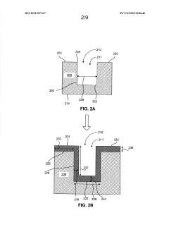
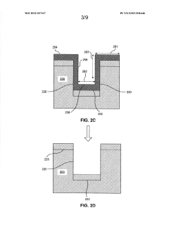
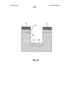
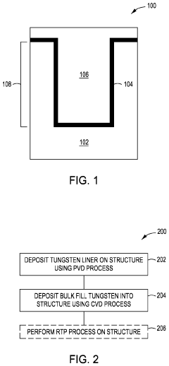
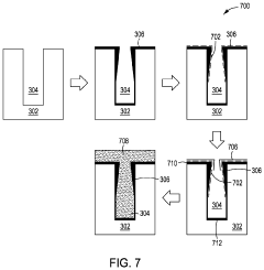
- A method involving physical vapor deposition (PVD) of tungsten with subsequent oxidation and removal steps to achieve selective deposition, where different thicknesses are controlled on the substrate field, sidewalls, and dielectric bottom surfaces, ensuring complete removal from sidewalls and retention on the dielectric bottom, facilitating uniform gap filling.
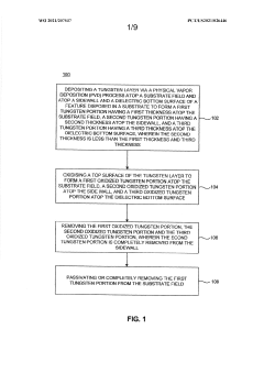
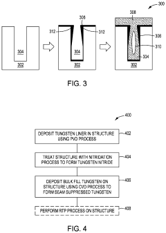
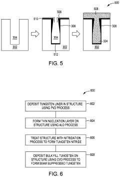
- The proposed method involves a physical vapor deposition of a tungsten liner, followed by an atomic layer deposition nucleation layer and a chemical vapor deposition bulk fill process, with a nitridation step and optional rapid thermal processing to reduce internal stresses and lower resistivity, using argon or krypton as ambient gases and optimizing temperature, pressure, and nitridation conditions.
Supply Chain Dynamics
The supply chain dynamics of tungsten-based technologies are complex and multifaceted, influenced by various factors including geopolitical considerations, market demands, and technological advancements. Tungsten, a critical raw material for many high-tech applications, has a concentrated supply chain with China dominating global production. This concentration creates potential vulnerabilities and price volatility in the market.
Recent years have seen increased efforts to diversify tungsten sources and reduce dependency on a single region. Countries like Vietnam, Russia, and Bolivia are emerging as alternative suppliers, though their production volumes are still relatively small compared to China. This diversification trend is driven by both strategic concerns and the need for supply stability in industries relying on tungsten-based technologies.
The recycling of tungsten has become an increasingly important aspect of the supply chain. Advanced recycling technologies are being developed to recover tungsten from scrap and used products, creating a more circular economy for this valuable resource. This not only helps in reducing supply risks but also aligns with global sustainability goals.
The processing and refining stages of the tungsten supply chain are also undergoing significant changes. Innovations in extraction and purification methods are improving efficiency and reducing environmental impact. These advancements are crucial for pushing the boundaries of tungsten-based technologies, as they enable the production of higher-quality materials with enhanced properties.
Demand fluctuations in key industries such as aerospace, automotive, and electronics significantly impact the tungsten supply chain. As these sectors continue to evolve and adopt new technologies, the demand for specialized tungsten products is expected to grow. This dynamic necessitates a more agile and responsive supply chain capable of adapting to rapidly changing market needs.
The development of new tungsten alloys and composites is also influencing supply chain dynamics. These advanced materials often require specific grades of tungsten or novel processing techniques, driving innovation throughout the supply chain. Suppliers and manufacturers are increasingly collaborating to develop tailored solutions that meet the exacting requirements of cutting-edge applications.
Environmental Impact
The environmental impact of tungsten-based technologies is a critical consideration as the industry pushes boundaries in this field. Tungsten mining and processing can have significant ecological consequences, including habitat destruction, soil erosion, and water pollution. The extraction process often involves open-pit mining, which can lead to landscape alterations and biodiversity loss. Furthermore, the refining of tungsten ore requires substantial energy inputs, contributing to greenhouse gas emissions and climate change concerns.
Water usage is another major environmental issue associated with tungsten production. The beneficiation process, which separates tungsten from other minerals, typically requires large volumes of water. This can strain local water resources, particularly in arid regions where tungsten deposits are often found. Additionally, the potential for acid mine drainage poses a long-term threat to surrounding ecosystems and groundwater quality.
As the demand for tungsten-based technologies grows, there is an increasing focus on developing more sustainable practices. Recycling and urban mining of tungsten from end-of-life products are becoming increasingly important strategies to reduce the environmental footprint of tungsten production. These approaches not only conserve natural resources but also minimize the need for new mining operations.
Innovations in processing technologies are also contributing to improved environmental performance. Advanced beneficiation techniques, such as gravity separation and flotation, are being optimized to reduce water and energy consumption. Moreover, research into bio-leaching and other environmentally friendly extraction methods shows promise for reducing the use of harsh chemicals in tungsten recovery.
The development of tungsten-based materials with enhanced durability and performance can indirectly benefit the environment by extending product lifespans and reducing the frequency of replacement. This approach aligns with circular economy principles and helps to minimize waste generation and resource depletion over time.
As the industry pushes boundaries in tungsten-based technologies, there is a growing emphasis on life cycle assessments to comprehensively evaluate environmental impacts from cradle to grave. This holistic approach enables manufacturers to identify and address environmental hotspots throughout the product lifecycle, leading to more sustainable design and production practices.