Tungsten-Driven Advancements In Optical Devices
Tungsten in Optics: Background and Objectives
Tungsten has played a pivotal role in the evolution of optical devices, marking significant milestones in the field of optics and photonics. The journey of tungsten in optical applications began with its use in incandescent light bulbs, where its high melting point and durability made it an ideal filament material. This initial application laid the foundation for further exploration of tungsten's potential in more advanced optical systems.
As technology progressed, the unique properties of tungsten, such as its high refractive index, excellent thermal stability, and resistance to wear, became increasingly valuable in the development of sophisticated optical devices. The metal's ability to withstand high temperatures while maintaining its optical properties opened up new possibilities in the design of optical coatings, mirrors, and other critical components in optical systems.
The objectives of tungsten-driven advancements in optical devices are multifaceted. Primarily, researchers and engineers aim to leverage tungsten's exceptional properties to enhance the performance, durability, and efficiency of optical systems. This includes improving the resolution and contrast of imaging devices, increasing the power handling capabilities of laser systems, and developing more robust optical coatings for extreme environments.
One of the key goals is to exploit tungsten's high refractive index to create novel optical structures and metamaterials. These advanced materials have the potential to manipulate light in unprecedented ways, leading to breakthroughs in fields such as super-resolution imaging, cloaking devices, and ultra-efficient solar cells. Additionally, tungsten's thermal properties make it an attractive candidate for thermal management in high-power optical systems, addressing critical challenges in laser technology and photonics.
The integration of tungsten into nanoscale optical devices represents another frontier in this field. Researchers are exploring the use of tungsten nanostructures to create plasmonic devices, which can confine and manipulate light at scales far below the diffraction limit. This opens up possibilities for ultra-compact optical sensors, high-density data storage, and advanced optical computing systems.
As we look to the future, the objectives of tungsten-driven optical advancements extend beyond traditional applications. There is growing interest in utilizing tungsten-based optical devices in quantum technologies, where its stability and unique optical properties could play a crucial role in developing quantum sensors and communication systems. Furthermore, the biocompatibility of certain tungsten compounds is driving research into their use in biomedical imaging and therapeutic applications.
In conclusion, the background and objectives of tungsten in optics reflect a rich history of innovation and a promising future of technological breakthroughs. From its humble beginnings in light bulbs to its potential role in quantum technologies, tungsten continues to be a key enabler in the advancement of optical devices, pushing the boundaries of what is possible in the manipulation and utilization of light.
Market Demand for Tungsten-Enhanced Optical Devices
The market demand for tungsten-enhanced optical devices has been steadily growing, driven by advancements in various industries and the unique properties of tungsten. This metal's high melting point, excellent thermal and electrical conductivity, and superior hardness make it an ideal material for enhancing the performance of optical devices.
In the semiconductor industry, tungsten-based optical components are increasingly sought after for lithography processes. As chip manufacturers push for smaller and more efficient designs, the demand for high-precision optical systems capable of operating at extreme ultraviolet (EUV) wavelengths has surged. Tungsten's ability to withstand high temperatures and resist wear makes it crucial for mirrors and other components in EUV lithography systems.
The aerospace and defense sectors have also shown a growing interest in tungsten-enhanced optical devices. Satellites and space-based telescopes require materials that can maintain their integrity in harsh environments. Tungsten's resistance to thermal expansion and its ability to withstand radiation make it an excellent choice for optical components in these applications. This has led to an increased demand for tungsten-coated mirrors and lenses in space exploration and Earth observation missions.
In the medical field, tungsten-enhanced optical devices are gaining traction in diagnostic and therapeutic equipment. The metal's high density and ability to block X-rays make it valuable in medical imaging systems. There is a rising demand for tungsten-based components in CT scanners, X-ray machines, and radiation therapy equipment, as healthcare providers seek more precise and efficient diagnostic tools.
The automotive industry is another sector driving the demand for tungsten-enhanced optical devices. As advanced driver-assistance systems (ADAS) and autonomous vehicles become more prevalent, there is a growing need for high-performance sensors and cameras. Tungsten's durability and resistance to harsh environmental conditions make it an attractive material for optical components in these systems, particularly for LiDAR and infrared sensors.
The global push for renewable energy has also contributed to the market demand for tungsten-enhanced optical devices. In solar energy applications, tungsten-based coatings are used to improve the efficiency of photovoltaic cells. The metal's ability to reflect infrared radiation while allowing visible light to pass through makes it valuable in creating more effective solar panels.
As industries continue to innovate and push the boundaries of technology, the demand for tungsten-enhanced optical devices is expected to grow further. The unique properties of tungsten make it an essential material for addressing the challenges of next-generation optical systems across various sectors, from advanced manufacturing to space exploration and healthcare.
Current State and Challenges in Tungsten Optics
The field of tungsten-based optical devices has witnessed significant advancements in recent years, with researchers and industry professionals pushing the boundaries of what is possible in optical technology. Currently, tungsten is being extensively explored for its unique properties that make it an ideal material for various optical applications.
One of the primary areas of focus is the development of tungsten-based photonic crystals. These structures exhibit exceptional control over light propagation and emission, making them valuable for applications in telecommunications and optical computing. However, challenges remain in achieving precise fabrication techniques that can reliably produce these complex nanostructures at scale.
In the realm of thermal emitters, tungsten has shown great promise due to its high melting point and stability at elevated temperatures. Researchers have successfully demonstrated tungsten-based selective thermal emitters that can efficiently convert heat into light, with potential applications in thermophotovoltaic energy conversion systems. Despite these advancements, improving the long-term stability and efficiency of these devices under extreme operating conditions remains a significant challenge.
Tungsten's role in plasmonic devices has also gained considerable attention. Its ability to support surface plasmon polaritons in the visible and near-infrared regions makes it an attractive material for developing novel sensing and imaging technologies. However, the high optical losses associated with tungsten at these wavelengths pose limitations that researchers are actively working to overcome.
In the field of metamaterials, tungsten-based structures have shown potential for creating devices with extraordinary optical properties, such as negative refractive index and perfect absorption. These developments open up possibilities for advanced optical cloaking and super-resolution imaging. The main challenges in this area include reducing fabrication complexities and extending the operational bandwidth of these devices.
Another promising application of tungsten in optics is the development of high-power laser mirrors. Tungsten's excellent thermal management properties make it an ideal candidate for mirror coatings in high-energy laser systems. However, improving the reflectivity and damage threshold of these coatings while maintaining their thermal stability remains an ongoing challenge.
The integration of tungsten into semiconductor optoelectronic devices is also an area of active research. Tungsten-based contacts and interconnects are being explored to enhance the performance of photodetectors and light-emitting diodes. Overcoming issues related to interface quality and compatibility with existing fabrication processes presents significant hurdles in this domain.
While the current state of tungsten optics shows great promise, several challenges persist across various applications. These include optimizing material properties, developing more efficient fabrication techniques, and improving device performance and reliability. Addressing these challenges will be crucial for realizing the full potential of tungsten-driven advancements in optical devices and paving the way for next-generation optical technologies.
Existing Tungsten-Driven Optical Solutions
01 Advanced optical imaging systems
Recent advancements in optical devices include improved imaging systems with enhanced resolution, sensitivity, and functionality. These systems incorporate novel optical components and processing techniques to achieve better performance in various applications such as medical imaging, industrial inspection, and scientific research.- Advanced optical imaging systems: Recent advancements in optical devices include improved imaging systems with enhanced resolution, sensitivity, and functionality. These systems incorporate novel optical components and processing techniques to achieve better performance in various applications such as medical imaging, surveillance, and scientific research.
- Optical communication technologies: Innovations in optical communication devices focus on increasing data transmission rates, improving signal quality, and extending communication range. These advancements include new designs for optical fibers, modulators, and receivers, as well as novel techniques for multiplexing and signal processing.
- Miniaturization and integration of optical components: Efforts to miniaturize and integrate optical components have led to the development of compact, multifunctional optical devices. These advancements enable the creation of smaller, more efficient systems for applications in consumer electronics, telecommunications, and sensing technologies.
- Adaptive and smart optical systems: Recent developments in adaptive and smart optical systems incorporate advanced materials, sensors, and control mechanisms to dynamically adjust optical properties. These innovations enable real-time optimization of optical performance in response to changing environmental conditions or user requirements.
- Quantum optical devices: Advancements in quantum optical devices leverage quantum mechanical principles to achieve unprecedented capabilities in sensing, computing, and secure communication. These innovations include the development of single-photon sources, detectors, and quantum memories for applications in quantum information processing and metrology.
02 Optical communication technologies
Innovations in optical communication devices focus on increasing data transmission rates, improving signal quality, and extending communication range. These advancements include novel optical fibers, modulators, and receivers that enable faster and more efficient data transfer in telecommunications and networking applications.Expand Specific Solutions03 Miniaturization of optical components
Ongoing efforts in miniaturization have led to the development of compact optical devices with improved performance. These advancements include the integration of multiple optical functions into single chips, reducing device size while maintaining or enhancing functionality for applications in consumer electronics, automotive, and aerospace industries.Expand Specific Solutions04 Adaptive and smart optical systems
Recent developments in adaptive and smart optical systems incorporate advanced materials and control mechanisms to dynamically adjust optical properties. These innovations enable real-time optimization of optical performance in response to changing environmental conditions or user requirements, enhancing the versatility and efficiency of optical devices.Expand Specific Solutions05 Integration of optical and electronic technologies
Advancements in the integration of optical and electronic technologies have led to the development of hybrid devices that combine the benefits of both domains. These innovations enable improved data processing, sensing, and communication capabilities in applications such as LiDAR, augmented reality, and quantum computing.Expand Specific Solutions
Key Players in Tungsten Optical Device Industry
The tungsten-driven advancements in optical devices market is in a growth phase, with increasing demand for high-performance optical components across various industries. The market size is expanding due to applications in electronics, lighting, and advanced imaging systems. Technologically, the field is progressing rapidly, with companies like Seiko Epson Corp., 3M Innovative Properties Co., and Semiconductor Energy Laboratory Co., Ltd. leading innovations. These firms are developing novel tungsten-based materials and manufacturing processes to enhance optical device performance. Other key players such as Merck Patent GmbH and Sumitomo Metal Mining Co. Ltd. are contributing to the technological maturity by focusing on material science advancements and production scalability, driving the industry towards more efficient and cost-effective solutions.
Semiconductor Energy Laboratory Co., Ltd.
Sumitomo Metal Mining Co. Ltd.
Core Innovations in Tungsten Optical Materials
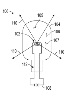
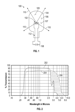
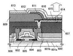
- Employing a tungsten-halogen electromagnetic radiation source with a polycrystalline aluminum oxynitride envelope that allows for a halogen regenerative cycle and the use of fluoride compounds, maintaining uniform filament thickness and enhancing spectral transmission.
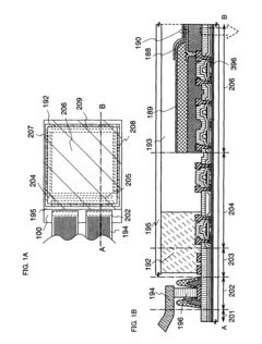
- The use of an indium zinc oxide film containing tungsten oxide, which is formed using gases like H2O or H2, and optionally silicon oxide, as a light-transmitting electrode layer in display devices, enhancing transmittance, low resistivity, and processability, and reducing defects through improved etching processes.
Environmental Impact of Tungsten in Optics
The environmental impact of tungsten in optical devices is a critical consideration as the use of this metal continues to expand in the field of optics. Tungsten's unique properties, including its high melting point and excellent thermal conductivity, make it an invaluable material for various optical applications. However, its extraction, processing, and disposal pose significant environmental challenges that must be addressed.
Mining and processing tungsten ore can lead to substantial environmental degradation. Open-pit mining, often used for tungsten extraction, results in large-scale land disturbance, habitat destruction, and potential water pollution. The energy-intensive refining process contributes to increased carbon emissions, exacerbating climate change concerns. Additionally, the use of chemicals in tungsten processing can lead to soil and water contamination if not properly managed.
In optical device manufacturing, tungsten's environmental footprint extends to the production phase. The high temperatures required for tungsten processing consume significant amounts of energy, primarily derived from fossil fuels. This energy consumption contributes to greenhouse gas emissions and air pollution. Furthermore, the production of tungsten-based optical components often involves the use of hazardous chemicals and generates toxic waste, which requires careful handling and disposal to prevent environmental contamination.
The longevity of tungsten-based optical devices presents both advantages and challenges from an environmental perspective. On one hand, the durability of tungsten components can lead to longer product lifespans, potentially reducing electronic waste. However, the difficulty in recycling tungsten from complex optical devices poses end-of-life management issues. Improper disposal of these devices can result in tungsten and associated materials leaching into soil and water systems, potentially harming ecosystems and human health.
To mitigate these environmental impacts, the optical industry is exploring several strategies. Efforts are being made to improve the efficiency of tungsten mining and processing, reducing energy consumption and minimizing waste. Research into alternative materials that can match tungsten's optical properties while having a lower environmental impact is ongoing. Additionally, advancements in recycling technologies are being pursued to better recover tungsten from end-of-life optical devices, promoting a more circular economy approach.
As the demand for high-performance optical devices continues to grow, balancing the technological benefits of tungsten with its environmental impact remains a crucial challenge. The industry must continue to innovate in sustainable practices, from responsible sourcing to improved manufacturing processes and effective recycling methods, to ensure that the advancements in optical devices do not come at an unacceptable environmental cost.
Tungsten Optics Manufacturing Processes
Tungsten optics manufacturing processes have evolved significantly over the years, driven by the increasing demand for high-performance optical devices. The production of tungsten-based optical components involves several sophisticated techniques, each tailored to specific applications and performance requirements.
One of the primary manufacturing methods is powder metallurgy, which allows for the creation of complex shapes with high precision. This process begins with the preparation of tungsten powder, followed by compaction and sintering. The sintering stage is crucial, as it determines the final density and microstructure of the component. Advanced sintering techniques, such as hot isostatic pressing (HIP), are often employed to achieve near-theoretical density and improved mechanical properties.
For applications requiring extremely smooth surfaces, such as mirrors or reflectors, precision machining and polishing techniques are essential. Computer Numerical Control (CNC) machining is widely used to shape tungsten components with high accuracy. This is followed by lapping and polishing processes, which can achieve surface roughness levels as low as a few nanometers. Chemical-mechanical polishing (CMP) is particularly effective for producing ultra-smooth tungsten surfaces.
Thin film deposition techniques play a vital role in creating tungsten-based optical coatings. Physical vapor deposition (PVD) methods, including sputtering and electron beam evaporation, are commonly used to deposit thin layers of tungsten on various substrates. These coatings can enhance reflectivity, durability, and other optical properties. For more complex structures, chemical vapor deposition (CVD) can be employed to create tungsten films with precise thickness control and excellent conformality.
In recent years, additive manufacturing technologies have begun to make inroads into tungsten optics production. Selective laser melting (SLM) and electron beam melting (EBM) show promise for creating complex tungsten structures with internal features that would be difficult or impossible to produce using traditional methods. However, these techniques are still in the early stages of development for tungsten, due to its high melting point and tendency to oxidize.
Surface modification techniques are often applied to enhance the performance of tungsten optical components. Plasma treatment can improve surface properties, while ion implantation can alter the near-surface composition to enhance durability or optical characteristics. Additionally, nanostructuring techniques, such as laser ablation or etching, can create specialized surface textures for light management or anti-reflective properties.
Quality control and characterization are integral parts of the manufacturing process. Advanced metrology tools, including interferometers, profilometers, and electron microscopes, are used to verify the dimensional accuracy and surface quality of tungsten optical components. X-ray diffraction and spectroscopic techniques help ensure the purity and crystalline structure of the tungsten material.