How To Innovate With Tungsten Nanostructure Applications?
Tungsten Nanostructure Evolution and Objectives
Tungsten nanostructures have emerged as a promising field of research and development, offering unique properties that could revolutionize various industries. The evolution of tungsten nanostructures can be traced back to the early 2000s when researchers began exploring the potential of nanoscale tungsten materials. Since then, significant advancements have been made in synthesis techniques, characterization methods, and application development.
The primary objective of tungsten nanostructure research is to harness the material's exceptional properties at the nanoscale. These properties include high melting point, excellent thermal and electrical conductivity, and superior mechanical strength. By manipulating tungsten at the nanoscale, researchers aim to enhance these inherent characteristics and unlock new functionalities that are not achievable with bulk tungsten.
One of the key goals in tungsten nanostructure development is to optimize the synthesis processes to achieve precise control over size, shape, and composition. This includes refining methods such as chemical vapor deposition, electrodeposition, and sol-gel techniques to produce high-quality, uniform nanostructures with tailored properties. Additionally, researchers are focusing on developing scalable production methods to bridge the gap between laboratory-scale synthesis and industrial-scale manufacturing.
Another important objective is to expand the application landscape of tungsten nanostructures. While traditional applications of tungsten have been primarily in lighting, electronics, and heavy industry, nanostructured tungsten opens up possibilities in fields such as energy storage, catalysis, and biomedical engineering. Researchers are actively exploring how tungsten nanostructures can be integrated into next-generation technologies, including advanced solar cells, fuel cells, and high-performance sensors.
The evolution of tungsten nanostructures is closely tied to advancements in characterization techniques. As such, a significant objective is to develop and refine analytical methods that can accurately probe the structural, chemical, and physical properties of these nanomaterials. This includes the use of advanced microscopy, spectroscopy, and computational modeling to gain deeper insights into the behavior of tungsten nanostructures at the atomic and molecular levels.
Environmental considerations and sustainability are also becoming increasingly important objectives in tungsten nanostructure research. Scientists are working on developing eco-friendly synthesis methods and exploring ways to recycle and reuse tungsten nanostructures to minimize environmental impact. This aligns with the broader trend towards green nanotechnology and sustainable materials development.
Looking ahead, the field of tungsten nanostructures is poised for continued growth and innovation. Future objectives include the development of multifunctional tungsten nanocomposites, the exploration of quantum effects in ultra-small tungsten nanostructures, and the integration of tungsten nanomaterials into smart and responsive systems. As research progresses, the goal is to translate these scientific advancements into practical applications that can address global challenges in energy, healthcare, and technology sectors.
Market Demand Analysis for Tungsten Nanostructures
The market demand for tungsten nanostructures has been steadily growing, driven by their unique properties and diverse applications across multiple industries. The global market for nanomaterials, including tungsten nanostructures, is projected to reach significant value in the coming years, with a compound annual growth rate (CAGR) exceeding industry averages.
In the electronics sector, tungsten nanostructures are gaining traction due to their exceptional thermal and electrical conductivity. As miniaturization continues to be a key trend in electronics, the demand for materials that can maintain performance at nanoscale dimensions is increasing. Tungsten nanostructures are being explored for use in advanced interconnects, heat sinks, and field emission devices, addressing the growing need for efficient thermal management and improved electrical performance in next-generation electronic devices.
The energy industry is another significant driver of demand for tungsten nanostructures. With the global push towards renewable energy and energy efficiency, tungsten nanostructures are being investigated for applications in solar cells, fuel cells, and energy storage devices. Their high melting point and resistance to corrosion make them attractive for use in harsh environments, such as those found in nuclear reactors and high-temperature fuel cells.
In the aerospace and defense sectors, tungsten nanostructures are sought after for their high strength-to-weight ratio and ability to withstand extreme conditions. These properties make them ideal for use in advanced composites, coatings, and armor materials. The growing emphasis on lightweight yet durable materials in aerospace applications is expected to further drive demand for tungsten nanostructures in this sector.
The medical field is also showing increased interest in tungsten nanostructures, particularly for their potential in imaging and therapeutic applications. Their high atomic number makes them excellent candidates for X-ray contrast agents, while their biocompatibility opens up possibilities for targeted drug delivery systems and cancer treatments.
Environmental applications represent an emerging market for tungsten nanostructures. Their catalytic properties are being explored for use in water purification systems and air pollution control technologies. As environmental regulations become more stringent globally, the demand for advanced materials capable of addressing these challenges is expected to grow.
Despite the promising market outlook, challenges remain in scaling up production and reducing costs associated with tungsten nanostructures. Current manufacturing processes can be complex and energy-intensive, which may limit widespread adoption in cost-sensitive applications. However, ongoing research and development efforts are focused on improving production efficiency and exploring new synthesis methods, which could potentially lower costs and expand market opportunities in the future.
Current Challenges in Tungsten Nanostructure Technology
Tungsten nanostructures represent a frontier in materials science, offering unique properties that could revolutionize various industries. However, the development and application of these nanostructures face several significant challenges that need to be addressed for their widespread adoption.
One of the primary challenges is the precise control of nanostructure morphology and size distribution. The properties of tungsten nanostructures are highly dependent on their dimensions and shapes, making it crucial to develop reliable and scalable synthesis methods. Current techniques often struggle to produce uniform nanostructures with consistent properties, limiting their potential applications.
Another major hurdle is the stability of tungsten nanostructures under extreme conditions. While tungsten is known for its high melting point and excellent thermal conductivity, nanostructures can exhibit different behaviors. Maintaining structural integrity and desired properties at high temperatures or in corrosive environments remains a significant challenge, particularly for applications in aerospace and nuclear industries.
The integration of tungsten nanostructures into existing systems and devices poses another set of challenges. Compatibility issues with other materials, potential agglomeration, and difficulties in achieving uniform dispersion in composites are common problems that researchers face. These integration challenges often hinder the practical implementation of tungsten nanostructures in real-world applications.
Cost-effective production of tungsten nanostructures at industrial scales is also a major concern. Current synthesis methods are often expensive, energy-intensive, or low-yield, making large-scale production economically unfeasible for many applications. Developing more efficient and scalable production techniques is crucial for the widespread adoption of tungsten nanostructures.
Furthermore, the potential environmental and health impacts of tungsten nanostructures are not yet fully understood. As with many nanomaterials, there are concerns about their long-term effects on human health and ecosystems. Addressing these safety concerns through comprehensive studies and developing appropriate handling and disposal protocols is essential for the responsible development of this technology.
Lastly, the characterization and quality control of tungsten nanostructures present significant technical challenges. Advanced analytical techniques are required to accurately assess the structure, composition, and properties of these nanomaterials. Developing standardized testing methods and quality assurance protocols is crucial for ensuring consistency and reliability in research and industrial applications.
Overcoming these challenges will require interdisciplinary collaboration, innovative research approaches, and significant investment in both fundamental science and applied engineering. As these hurdles are addressed, the potential for tungsten nanostructures to enable breakthrough technologies in fields such as energy, electronics, and materials science will continue to grow.
Existing Tungsten Nanostructure Applications
01 Synthesis methods for tungsten nanostructures
Various methods are employed to synthesize tungsten nanostructures, including chemical vapor deposition, electrodeposition, and solution-based techniques. These processes allow for the controlled growth of nanostructures with different morphologies such as nanowires, nanoparticles, and nanotubes. The synthesis parameters can be adjusted to tailor the size, shape, and properties of the resulting nanostructures.- Synthesis methods for tungsten nanostructures: Various methods are employed to synthesize tungsten nanostructures, including chemical vapor deposition, electrodeposition, and solution-based techniques. These processes allow for the controlled growth of nanostructures with different morphologies such as nanowires, nanoparticles, and nanotubes. The synthesis parameters can be adjusted to tailor the size, shape, and properties of the resulting nanostructures.
- Applications in electronic devices: Tungsten nanostructures find applications in various electronic devices due to their unique properties. They are used in field emission displays, electron sources, and as interconnects in microelectronics. The high conductivity and thermal stability of tungsten nanostructures make them suitable for use in high-performance electronic components and sensors.
- Catalytic applications: Tungsten nanostructures exhibit excellent catalytic properties, making them valuable in various chemical reactions. They are used as catalysts in hydrogenation reactions, fuel cells, and environmental remediation processes. The high surface area and unique electronic properties of tungsten nanostructures contribute to their enhanced catalytic activity compared to bulk tungsten.
- Structural reinforcement in composites: Tungsten nanostructures are incorporated into composite materials to enhance their mechanical and thermal properties. These nanostructures can improve the strength, stiffness, and wear resistance of the composite materials. Applications include aerospace components, armor materials, and high-performance sporting goods.
- Energy storage and conversion: Tungsten nanostructures play a role in energy storage and conversion technologies. They are used in the development of advanced batteries, supercapacitors, and hydrogen storage materials. The high surface area and unique electronic properties of tungsten nanostructures contribute to improved energy storage capacity and efficiency in these applications.
02 Applications in electronic devices
Tungsten nanostructures find applications in various electronic devices due to their unique properties. They are used in field emission displays, sensors, and as interconnects in microelectronics. The high electrical conductivity and thermal stability of tungsten nanostructures make them suitable for these applications, potentially improving device performance and reliability.Expand Specific Solutions03 Energy storage and conversion applications
Tungsten nanostructures are explored for energy-related applications, including catalysts for fuel cells, electrodes for batteries, and materials for hydrogen storage. Their high surface area and catalytic properties make them promising candidates for improving the efficiency of energy storage and conversion devices.Expand Specific Solutions04 Surface modification and functionalization
Techniques for modifying the surface of tungsten nanostructures are developed to enhance their properties or add new functionalities. This includes coating with other materials, doping, or attaching functional groups. Such modifications can improve the nanostructures' performance in specific applications or enable their use in new fields.Expand Specific Solutions05 Characterization and analysis techniques
Advanced characterization methods are employed to study the properties and structure of tungsten nanostructures. These include electron microscopy, X-ray diffraction, and spectroscopic techniques. Such analyses are crucial for understanding the relationship between the nanostructures' synthesis conditions, morphology, and resulting properties, enabling the optimization of their performance in various applications.Expand Specific Solutions
Key Players in Tungsten Nanostructure Industry
The innovation landscape for tungsten nanostructure applications is in a dynamic growth phase, with a rapidly expanding market driven by advancements in materials science and nanotechnology. The global market for tungsten nanostructures is projected to grow significantly, fueled by increasing demand in electronics, energy storage, and biomedical sectors. Technologically, the field is progressing from early-stage research to more applied developments, with companies like Chongyi Zhangyuan Tungsten Co., Ltd. and Xi'an Rare Metal Materials Research Institute Co., Ltd. leading commercial efforts. Academic institutions such as The Regents of the University of California and Beijing University of Technology are pushing the boundaries of fundamental research, while industry players like PPG Industries Ohio, Inc. and Corning, Inc. are focusing on practical applications and scalable production methods.
Chongyi Zhangyuan Tungsten Co., Ltd.
Xi'an Rare Metal Materials Research Institute Co., Ltd.
Breakthrough Innovations in Tungsten Nanostructures
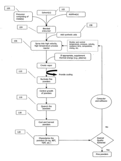
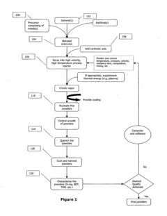
- The development of methods for producing high-purity nanoscale and submicron powders using tungsten-containing precursors, involving high-temperature processing, quenching, and recycling of by-products, to create doped or undoped tungsten oxides and composites with tailored morphology and properties for various applications.
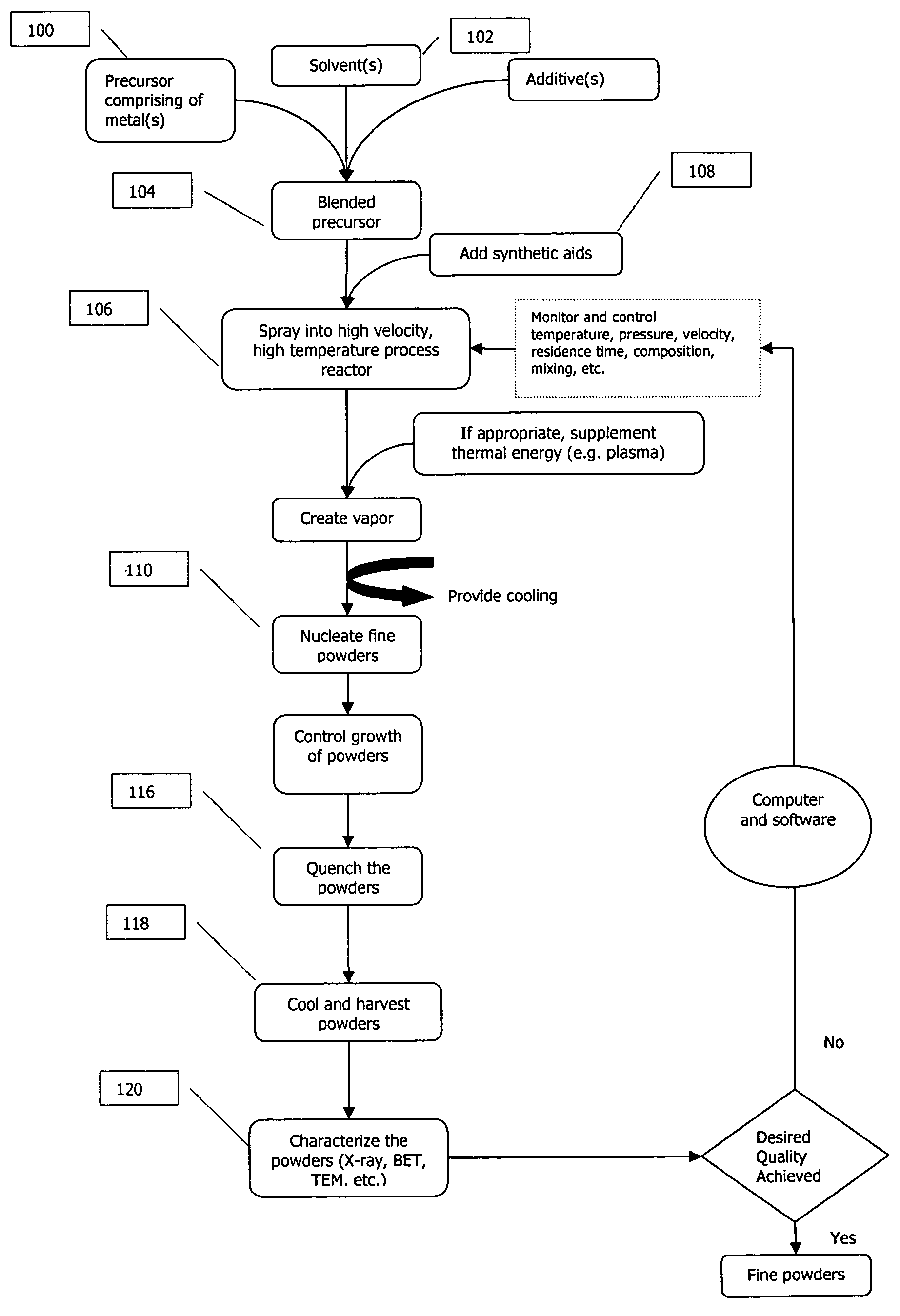
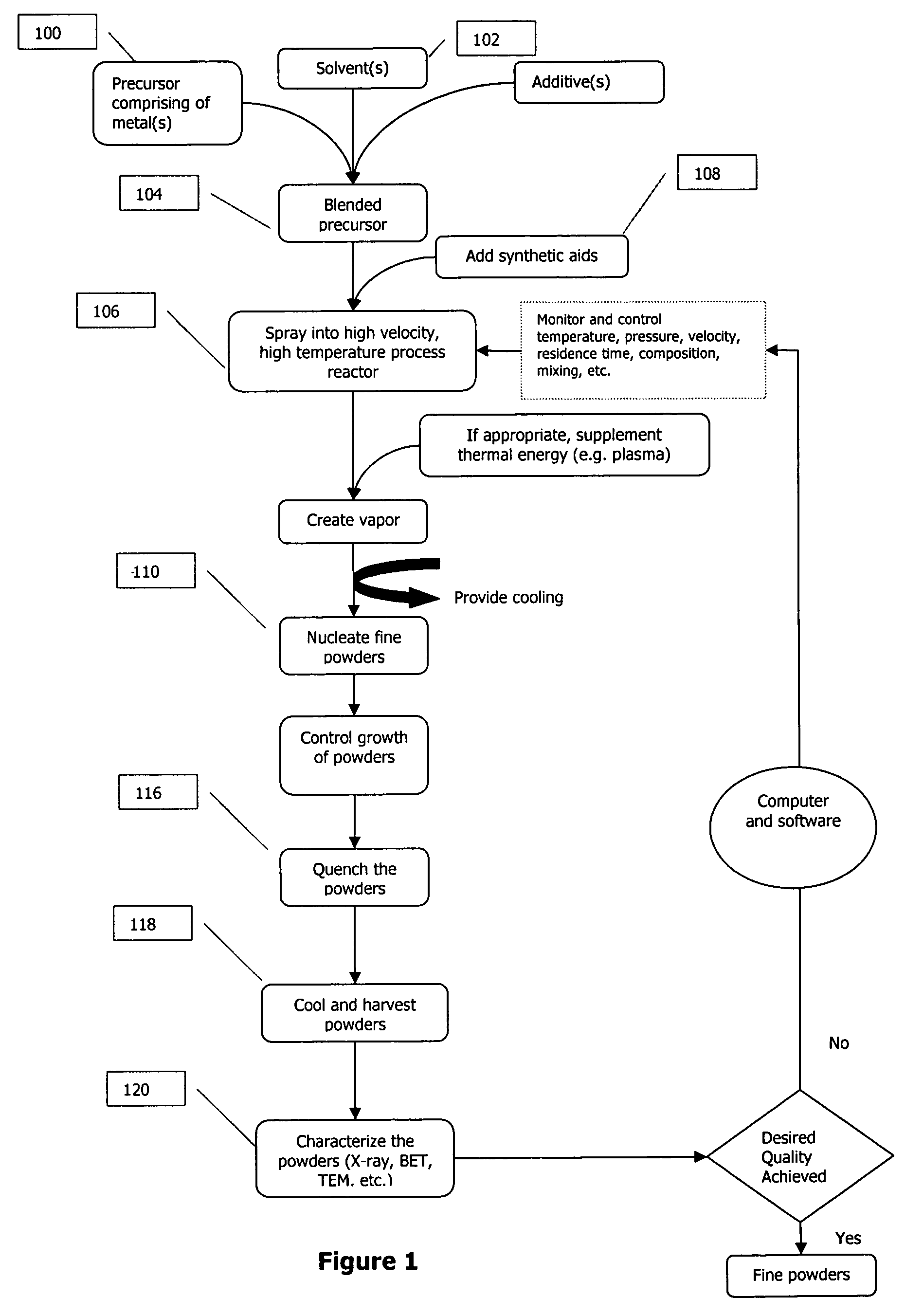
- The development of methods for producing high-purity nanoscale and submicron powders using tungsten-containing precursors, involving high-temperature processing, quenching, and recycling of by-products, to create doped or undoped tungsten oxides and composites with tailored morphology and properties for various applications.
Environmental Impact of Tungsten Nanostructures
The environmental impact of tungsten nanostructures is a critical consideration in their development and application. These nanostructures, while offering significant technological advancements, also pose potential risks to ecosystems and human health. The production process of tungsten nanostructures often involves energy-intensive methods and the use of hazardous chemicals, which can contribute to air and water pollution if not properly managed.
One of the primary environmental concerns is the potential release of tungsten nanoparticles into the environment. These particles, due to their small size, can easily disperse in air and water, potentially entering food chains and ecosystems. Studies have shown that tungsten nanoparticles can accumulate in plants and aquatic organisms, potentially leading to bioaccumulation in higher trophic levels.
The toxicity of tungsten nanostructures to various organisms is an area of ongoing research. While bulk tungsten is generally considered inert, nanostructures may exhibit different properties due to their increased surface area and reactivity. Some studies have indicated potential cytotoxicity and genotoxicity in certain cell lines, raising concerns about long-term exposure effects on both wildlife and human populations.
Water contamination is another significant environmental issue associated with tungsten nanostructures. The high solubility of some tungsten compounds in water can lead to the spread of these materials through aquatic systems. This can potentially affect water quality and aquatic life, particularly in areas near production facilities or where tungsten-based products are heavily used.
However, it's important to note that the environmental impact of tungsten nanostructures is not entirely negative. Their use in certain applications, such as catalysts for environmental remediation or in more efficient energy technologies, can potentially lead to positive environmental outcomes. For instance, tungsten nanostructures used in catalytic converters can improve air quality by more effectively reducing harmful emissions.
To mitigate the potential negative environmental impacts, researchers and industries are focusing on developing more sustainable production methods and safer handling practices for tungsten nanostructures. This includes exploring green synthesis techniques, improving containment strategies during production and use, and developing effective methods for the detection and removal of tungsten nanoparticles from the environment.
As the field of nanotechnology continues to advance, ongoing research into the environmental fate and effects of tungsten nanostructures is crucial. This will help in developing appropriate regulatory frameworks and guidelines for their safe production, use, and disposal, ensuring that the benefits of these innovative materials can be realized while minimizing their environmental footprint.
Scalability and Manufacturing Challenges
The scalability and manufacturing challenges associated with tungsten nanostructure applications present significant hurdles in their widespread adoption and commercialization. One of the primary obstacles is the difficulty in producing large quantities of uniform tungsten nanostructures with consistent properties. Current synthesis methods, such as chemical vapor deposition and electrodeposition, often struggle to maintain precise control over nanostructure size, shape, and composition when scaled up to industrial levels.
Another challenge lies in the integration of tungsten nanostructures into existing manufacturing processes. Many potential applications, such as in electronics or energy storage, require seamless incorporation of these nanostructures into complex devices or systems. This integration often demands the development of new manufacturing techniques or the modification of existing ones, which can be both time-consuming and costly.
The high melting point and hardness of tungsten also pose challenges in processing and shaping nanostructures for specific applications. Traditional machining methods may not be suitable for manipulating tungsten at the nanoscale, necessitating the development of specialized techniques that can maintain the unique properties of the nanostructures while achieving desired forms and configurations.
Cost-effectiveness is another critical factor in scaling up tungsten nanostructure production. The raw materials and energy requirements for synthesizing these nanostructures can be substantial, potentially limiting their economic viability for certain applications. Developing more efficient synthesis methods and optimizing resource utilization are crucial steps in addressing this challenge.
Quality control and characterization of tungsten nanostructures at industrial scales present additional hurdles. Ensuring consistent properties and performance across large batches requires advanced analytical techniques and robust quality assurance protocols. This is particularly important for applications in sensitive fields such as aerospace or medical devices, where reliability and reproducibility are paramount.
Environmental and safety considerations also play a significant role in scaling up tungsten nanostructure manufacturing. The potential health and environmental impacts of nanoparticles necessitate stringent safety measures and waste management protocols, which can add complexity and cost to the manufacturing process.
Addressing these scalability and manufacturing challenges will require collaborative efforts between materials scientists, engineers, and industry partners. Innovations in synthesis techniques, process automation, and quality control methods will be essential in overcoming these obstacles and realizing the full potential of tungsten nanostructure applications across various sectors.