How To Utilize Tungsten For Optoelectronic Advancements?
Tungsten Optoelectronics Background and Objectives
Tungsten, a refractory metal with exceptional properties, has been a subject of interest in the field of optoelectronics for decades. Its high melting point, excellent thermal stability, and unique electronic structure make it a promising candidate for various optoelectronic applications. The evolution of tungsten in optoelectronics can be traced back to its initial use in incandescent light bulbs, where its ability to withstand high temperatures made it an ideal filament material.
As technology progressed, researchers began exploring tungsten's potential in more advanced optoelectronic devices. The development of thin-film deposition techniques allowed for the creation of tungsten-based coatings and nanostructures, opening up new avenues for its application in photovoltaics, light-emitting diodes (LEDs), and photodetectors. The discovery of tungsten's plasmonic properties in the infrared region further expanded its potential in optoelectronic devices operating at longer wavelengths.
Recent advancements in nanotechnology have led to the synthesis of tungsten nanostructures, such as nanowires and nanoparticles, which exhibit enhanced optical and electronic properties compared to their bulk counterparts. These nanostructures have shown promise in improving the efficiency of solar cells, enhancing the performance of photodetectors, and enabling novel sensing applications.
The primary objective of utilizing tungsten for optoelectronic advancements is to leverage its unique properties to develop more efficient, durable, and versatile devices. Researchers aim to exploit tungsten's high melting point and thermal stability to create optoelectronic components that can operate reliably under extreme conditions, such as in space applications or high-temperature environments.
Another key goal is to harness tungsten's plasmonic properties to enhance light absorption and emission in optoelectronic devices. This could lead to the development of more sensitive photodetectors, higher-efficiency solar cells, and improved light-emitting devices. Additionally, researchers are exploring ways to integrate tungsten with other materials to create hybrid structures with superior optoelectronic properties.
The development of novel fabrication techniques for tungsten-based nanostructures and thin films is also a crucial objective. These advancements could enable the creation of more complex and efficient optoelectronic devices, potentially revolutionizing fields such as telecommunications, energy harvesting, and sensing technologies.
As the field of optoelectronics continues to evolve, the utilization of tungsten presents both challenges and opportunities. Overcoming limitations such as its high work function and optimizing its integration with other materials are key areas of focus. The successful realization of tungsten-based optoelectronic advancements has the potential to significantly impact various industries, from renewable energy to advanced imaging and sensing technologies.
Market Analysis for Tungsten-Based Optoelectronic Devices
The market for tungsten-based optoelectronic devices is experiencing significant growth, driven by the increasing demand for high-performance electronic and photonic components across various industries. Tungsten's unique properties, including its high melting point, excellent thermal conductivity, and superior mechanical strength, make it an attractive material for optoelectronic applications.
In the semiconductor industry, tungsten is widely used in the fabrication of integrated circuits and microchips. The global semiconductor market, valued at $556 billion in 2021, is projected to reach $1 trillion by 2030, indicating substantial growth potential for tungsten-based optoelectronic devices. The increasing adoption of advanced technologies such as 5G, artificial intelligence, and Internet of Things (IoT) is fueling this market expansion.
The automotive sector represents another significant market for tungsten-based optoelectronic devices. With the rise of electric vehicles and autonomous driving technologies, there is a growing need for advanced sensors, displays, and lighting systems. The global automotive electronics market is expected to grow at a CAGR of 7.9% from 2021 to 2028, presenting ample opportunities for tungsten-based optoelectronic components.
In the aerospace and defense industries, tungsten-based optoelectronic devices find applications in radar systems, infrared sensors, and communication equipment. The global aerospace and defense market is projected to reach $1,098 billion by 2026, with a CAGR of 7.7% from 2021 to 2026. This growth is driven by increasing defense budgets and the modernization of military equipment, creating a steady demand for advanced optoelectronic components.
The medical and healthcare sector is another promising market for tungsten-based optoelectronic devices. Applications include medical imaging systems, surgical instruments, and diagnostic equipment. The global medical devices market is expected to grow at a CAGR of 5.4% from 2021 to 2028, reaching $719 billion by 2028. The increasing focus on early disease detection and minimally invasive procedures is driving the demand for advanced optoelectronic devices in this sector.
Emerging technologies such as quantum computing and photonics are also creating new opportunities for tungsten-based optoelectronic devices. These fields require materials with exceptional properties for developing high-performance components, positioning tungsten as a key material for future innovations.
However, the market for tungsten-based optoelectronic devices faces challenges such as the volatility of tungsten prices and environmental concerns associated with tungsten mining and processing. Developing sustainable sourcing and production methods will be crucial for long-term market growth and acceptance.
Current Challenges in Tungsten Optoelectronic Applications
Despite the promising potential of tungsten in optoelectronic applications, several significant challenges currently hinder its widespread adoption and full utilization. One of the primary obstacles is the inherent material properties of tungsten, particularly its high melting point and hardness. While these characteristics make tungsten ideal for certain applications, they also present difficulties in processing and fabrication for optoelectronic devices.
The integration of tungsten into existing optoelectronic manufacturing processes poses a considerable challenge. Traditional semiconductor fabrication techniques often struggle to effectively incorporate tungsten due to its unique physical properties. This incompatibility leads to increased production costs and reduced scalability, limiting the commercial viability of tungsten-based optoelectronic devices.
Another significant hurdle is the optimization of tungsten's optical properties for specific optoelectronic applications. While tungsten exhibits promising characteristics in certain wavelength ranges, fine-tuning its performance across the entire spectrum of optoelectronic applications remains a complex task. This challenge is particularly evident in areas such as light emission and detection, where precise control over optical properties is crucial.
The development of efficient and stable tungsten-based thin films and nanostructures presents another major challenge. Creating uniform and defect-free tungsten layers at the nanoscale is essential for many optoelectronic applications, but achieving this consistently and cost-effectively remains difficult. The high surface energy of tungsten often leads to agglomeration and non-uniform growth, impacting device performance and reliability.
Thermal management is a critical issue in tungsten-based optoelectronic devices. The high operating temperatures often associated with tungsten components can lead to performance degradation and reduced device lifespan. Developing effective heat dissipation strategies without compromising the optical and electrical properties of the devices is a significant engineering challenge.
The environmental impact and sustainability of tungsten production and processing for optoelectronic applications are also growing concerns. As the demand for optoelectronic devices increases, addressing the environmental footprint of tungsten extraction and refinement becomes increasingly important. Developing more sustainable and eco-friendly methods for tungsten production and recycling is crucial for its long-term viability in the optoelectronics industry.
Lastly, there is a need for more comprehensive understanding and modeling of tungsten's behavior in complex optoelectronic systems. The interaction between tungsten and other materials in multilayer structures, as well as its long-term stability under various operating conditions, requires further research and development. Accurate simulation tools and predictive models are essential for optimizing device designs and reducing development cycles.
Existing Tungsten Optoelectronic Solutions
01 Tungsten deposition methods
Various methods for depositing tungsten on substrates, including chemical vapor deposition (CVD) and atomic layer deposition (ALD). These techniques are used to create thin films of tungsten for applications in semiconductor manufacturing and other industries.- Tungsten deposition methods: Various methods for depositing tungsten on substrates, including chemical vapor deposition (CVD) and atomic layer deposition (ALD). These techniques are used to create thin films of tungsten for applications in semiconductor manufacturing and other industries.
- Tungsten etching processes: Techniques for selectively etching tungsten layers in semiconductor fabrication. These processes are crucial for creating precise patterns and structures in integrated circuits and other microelectronic devices.
- Tungsten alloys and composites: Development of tungsten-based alloys and composite materials with enhanced properties. These materials combine tungsten with other elements to improve characteristics such as strength, hardness, and thermal stability for various industrial applications.
- Tungsten in lighting applications: Use of tungsten in lighting technologies, particularly in filaments for incandescent and halogen lamps. The high melting point and durability of tungsten make it ideal for these applications.
- Tungsten in electronic components: Application of tungsten in various electronic components, including interconnects, electrodes, and heat sinks. Tungsten's properties, such as high electrical conductivity and thermal stability, make it valuable in advanced electronic devices.
02 Tungsten-based alloys and composites
Development of tungsten-based alloys and composite materials with enhanced properties, such as improved strength, hardness, and thermal stability. These materials find applications in aerospace, defense, and high-temperature industrial processes.Expand Specific Solutions03 Tungsten in semiconductor devices
Utilization of tungsten in semiconductor devices, including its use as interconnects, gate electrodes, and diffusion barriers. Tungsten's low resistivity and high melting point make it suitable for various semiconductor applications.Expand Specific Solutions04 Tungsten processing and recycling
Methods for processing tungsten ores, refining tungsten, and recycling tungsten-containing materials. These processes aim to improve the efficiency of tungsten production and reduce environmental impact.Expand Specific Solutions05 Tungsten in lighting applications
Use of tungsten in lighting applications, particularly in incandescent and halogen lamps. Tungsten filaments are widely used due to their high melting point and ability to withstand high temperatures, making them suitable for producing light through incandescence.Expand Specific Solutions
Key Players in Tungsten Optoelectronics Industry
The utilization of tungsten for optoelectronic advancements is in a growth phase, with increasing market size and technological maturity. The industry is experiencing rapid development due to tungsten's unique properties in optoelectronic applications. Major players like Applied Materials, Inc., Toshiba Corp., and Panasonic Holdings Corp. are driving innovation in this field. The technology's maturity is evident from the involvement of diverse companies, including semiconductor manufacturers like Taiwan Semiconductor Manufacturing Co., Ltd., and materials specialists such as Sumitomo Metal Mining Co. Ltd. and BASF Corp. Research institutions like the University of Science & Technology Beijing and the Colorado School of Mines are also contributing to advancements, indicating a collaborative ecosystem that is pushing the boundaries of tungsten's optoelectronic applications.
Applied Materials, Inc.
Toshiba Corp.
Core Innovations in Tungsten Optoelectronics
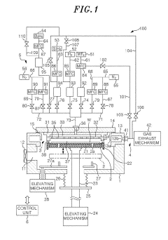
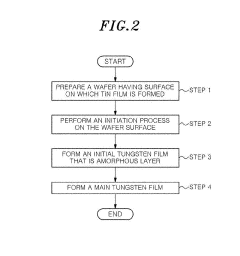
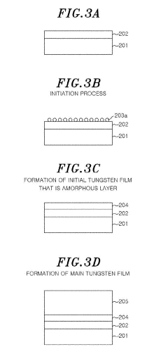
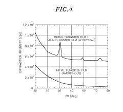
- A method involving the formation of a tungsten film on an amorphous layer, where an initial amorphous or crystalline tungsten film is created using WF6 and a reducing gas like H2, B2H6, or SiH4, followed by a main tungsten film deposition using WF6 and H2, to increase crystal grain size and reduce resistance.
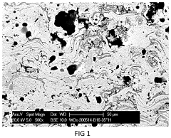
- A thick, lamellar structure tungsten oxide target with high tungsten oxide content and controlled oxygen deficiency, allowing for stable and conductive sputtering with reduced arcing and increased dynamic deposition rate, enabling efficient deposition of tungsten oxide layers.
Environmental Impact of Tungsten in Optoelectronics
The utilization of tungsten in optoelectronic advancements brings significant environmental considerations that must be carefully evaluated. Tungsten mining and processing can have substantial ecological impacts, including habitat disruption, soil erosion, and water pollution. The extraction process often involves open-pit mining, which can lead to deforestation and landscape alteration. Additionally, the refining of tungsten ore requires energy-intensive processes, contributing to greenhouse gas emissions and climate change concerns.
However, the use of tungsten in optoelectronics also presents potential environmental benefits. Tungsten-based components in optoelectronic devices often contribute to improved energy efficiency and longer product lifespans. This can lead to reduced electronic waste and lower overall energy consumption, mitigating some of the environmental impacts associated with electronic device production and disposal.
The production of tungsten-based optoelectronic components involves the use of various chemicals and processes that may pose environmental risks if not properly managed. Proper handling, treatment, and disposal of waste materials are crucial to prevent soil and water contamination. Implementing closed-loop manufacturing systems and adopting cleaner production technologies can significantly reduce the environmental footprint of tungsten-based optoelectronic manufacturing.
Recycling and recovery of tungsten from end-of-life optoelectronic devices present both challenges and opportunities. While tungsten is highly recyclable, the complex nature of modern electronic devices can make separation and recovery difficult. Developing efficient recycling technologies and establishing robust collection systems are essential for minimizing the environmental impact of tungsten use in optoelectronics and reducing the need for primary tungsten extraction.
The environmental impact of tungsten in optoelectronics extends to the entire product lifecycle, from raw material extraction to device disposal. Life cycle assessments (LCAs) are crucial for understanding and quantifying these impacts. LCAs can help identify hotspots in the production chain where environmental improvements can be made, guiding the development of more sustainable optoelectronic technologies.
As the demand for optoelectronic devices continues to grow, it is imperative to balance technological advancements with environmental stewardship. This requires a multifaceted approach, including sustainable mining practices, cleaner production methods, efficient recycling systems, and the development of alternative materials that can complement or replace tungsten in certain applications while maintaining or improving device performance.
Tungsten Optoelectronics Manufacturing Processes
The manufacturing processes for tungsten optoelectronics involve several sophisticated techniques that leverage the unique properties of this refractory metal. One of the primary methods is physical vapor deposition (PVD), which allows for the creation of thin tungsten films on various substrates. This process typically involves sputtering or electron beam evaporation in a high-vacuum environment, enabling precise control over film thickness and composition.
Chemical vapor deposition (CVD) is another crucial technique in tungsten optoelectronics manufacturing. This method utilizes gaseous precursors, such as tungsten hexafluoride (WF6), which react or decompose on the substrate surface to form a solid tungsten layer. CVD offers excellent conformality and can produce high-purity tungsten films, making it ideal for complex optoelectronic device structures.
Photolithography plays a vital role in patterning tungsten structures for optoelectronic applications. This process involves coating the tungsten layer with a photoresist, exposing it to light through a mask, and then selectively etching the exposed areas. Advanced lithography techniques, such as electron beam lithography, enable the creation of nanoscale tungsten features essential for cutting-edge optoelectronic devices.
Etching processes are critical for shaping tungsten structures in optoelectronic devices. Both wet and dry etching methods are employed, with reactive ion etching (RIE) being particularly useful for achieving high aspect ratio features. Plasma-based etching techniques offer excellent control over etch profiles and selectivity, crucial for maintaining device performance.
Surface modification and functionalization of tungsten are often necessary to enhance its optoelectronic properties. Techniques such as ion implantation, thermal oxidation, and plasma treatment can be used to alter the surface chemistry and electronic structure of tungsten, tailoring its characteristics for specific optoelectronic applications.
Integration of tungsten with other materials is a key aspect of optoelectronic device fabrication. This may involve depositing dielectric layers, forming metal contacts, or creating heterostructures with semiconductors. Techniques like atomic layer deposition (ALD) are particularly useful for creating ultra-thin, conformal layers in complex device architectures.
Quality control and characterization are integral to the manufacturing process. Techniques such as X-ray diffraction (XRD), scanning electron microscopy (SEM), and atomic force microscopy (AFM) are employed to assess film quality, thickness, and surface morphology. Electrical and optical characterization methods are also crucial for evaluating device performance and ensuring consistency in production.