New Frontiers In Tungsten Semiconductor Technology
Tungsten Semiconductor Evolution and Objectives
Tungsten semiconductor technology has emerged as a promising frontier in the field of advanced electronics, offering potential solutions to the limitations of traditional silicon-based semiconductors. The evolution of tungsten semiconductors can be traced back to the early 2000s when researchers began exploring alternative materials to overcome the scaling challenges faced by silicon technology.
The primary objective of tungsten semiconductor research is to develop high-performance, energy-efficient devices capable of operating at higher frequencies and temperatures than their silicon counterparts. This technology aims to address the increasing demand for faster, more powerful, and more compact electronic systems in various applications, including telecommunications, aerospace, and high-performance computing.
Over the past two decades, significant progress has been made in understanding the unique properties of tungsten-based semiconductors. These materials exhibit exceptional thermal stability, high electron mobility, and superior electrical conductivity compared to silicon. These characteristics make tungsten semiconductors particularly attractive for applications requiring high-frequency operation and resistance to harsh environments.
One of the key milestones in the evolution of tungsten semiconductor technology was the development of tungsten diselenide (WSe2) as a two-dimensional material. This breakthrough, achieved in the early 2010s, opened up new possibilities for creating ultra-thin, flexible electronic devices with enhanced performance. Researchers have since focused on optimizing the growth and fabrication processes for tungsten-based semiconductors, aiming to improve their quality and scalability for commercial applications.
The current objectives in tungsten semiconductor research are multifaceted. Scientists and engineers are working towards enhancing the material's electrical properties, developing more efficient manufacturing techniques, and exploring novel device architectures that can fully leverage the unique characteristics of tungsten semiconductors. Additionally, there is a strong focus on integrating tungsten-based materials with existing silicon technology to create hybrid systems that combine the best of both worlds.
Looking ahead, the field of tungsten semiconductor technology is poised for further advancements. Researchers are exploring new compounds and alloys based on tungsten, aiming to discover materials with even more favorable properties. The development of advanced fabrication techniques, such as atomic layer deposition and molecular beam epitaxy, is expected to play a crucial role in realizing the full potential of tungsten semiconductors.
As the technology continues to mature, the objectives extend beyond pure research into practical applications. The semiconductor industry is closely watching the progress of tungsten-based devices, with the potential to revolutionize areas such as high-frequency communications, power electronics, and quantum computing. The ultimate goal is to establish tungsten semiconductors as a viable and superior alternative to silicon in specific application domains, paving the way for the next generation of electronic devices and systems.
Market Demand Analysis for Tungsten-based Semiconductors
The market demand for tungsten-based semiconductors is experiencing a significant upward trajectory, driven by the increasing need for high-performance electronic devices in various sectors. As traditional silicon-based semiconductors approach their physical limits, tungsten-based alternatives are gaining traction due to their superior electrical and thermal properties.
In the consumer electronics market, there is a growing demand for faster, more efficient devices with longer battery life. Tungsten-based semiconductors offer the potential to meet these requirements, particularly in smartphones, tablets, and wearable technology. The global smartphone market, valued at over $400 billion, is a key driver for this demand, with manufacturers constantly seeking ways to improve device performance and energy efficiency.
The automotive industry is another significant market for tungsten-based semiconductors. With the rapid growth of electric vehicles (EVs) and advanced driver-assistance systems (ADAS), there is an increasing need for high-performance, heat-resistant semiconductors. The global EV market, projected to reach $800 billion by 2027, represents a substantial opportunity for tungsten semiconductor technology.
In the aerospace and defense sectors, tungsten-based semiconductors are gaining attention due to their ability to withstand extreme conditions and provide enhanced performance in critical applications. The global aerospace and defense market, valued at over $1.5 trillion, is driving demand for advanced semiconductor technologies that can meet stringent reliability and performance requirements.
The data center and cloud computing industry is another key market for tungsten-based semiconductors. As data processing demands continue to grow exponentially, there is a need for more efficient and powerful semiconductors that can handle increased workloads while minimizing energy consumption. The global data center market, expected to reach $350 billion by 2026, presents a significant opportunity for tungsten semiconductor technology.
Industrial applications, including robotics, automation, and Internet of Things (IoT) devices, are also contributing to the market demand for tungsten-based semiconductors. These sectors require robust, high-performance components that can operate reliably in challenging environments.
The global semiconductor market, projected to exceed $600 billion by 2025, is showing increased interest in alternative materials like tungsten. However, the adoption of tungsten-based semiconductors faces challenges such as higher production costs and the need for new manufacturing processes. Despite these hurdles, the potential benefits in terms of performance, efficiency, and reliability are driving continued research and development efforts.
As environmental concerns grow, the energy efficiency advantages of tungsten-based semiconductors are becoming increasingly attractive. This aligns with global initiatives to reduce carbon emissions and improve energy sustainability across various industries.
Current State and Challenges in Tungsten Semiconductor Technology
Tungsten semiconductor technology has made significant strides in recent years, positioning itself as a promising alternative to traditional silicon-based semiconductors. The current state of tungsten semiconductor technology is characterized by a blend of achievements and ongoing challenges that researchers and industry players are actively addressing.
One of the primary advantages of tungsten semiconductors is their superior thermal conductivity, which allows for more efficient heat dissipation in high-power electronic devices. This property has led to increased interest in tungsten-based materials for applications in power electronics and high-frequency devices. Additionally, tungsten's high melting point and resistance to wear make it an attractive option for harsh environment applications, such as aerospace and automotive industries.
Despite these advantages, the widespread adoption of tungsten semiconductor technology faces several challenges. One of the most significant hurdles is the complexity of manufacturing processes. Unlike silicon, which has well-established fabrication techniques, tungsten semiconductors require specialized equipment and processes that are not yet fully optimized for large-scale production. This results in higher manufacturing costs and limited availability of tungsten-based semiconductor devices.
Another challenge lies in the integration of tungsten semiconductors with existing silicon-based technologies. While tungsten offers superior performance in certain aspects, the semiconductor industry's infrastructure is heavily geared towards silicon. Developing compatible interfaces and ensuring seamless integration with current technologies remains a critical area of research and development.
The electronic properties of tungsten semiconductors also present both opportunities and challenges. While they exhibit excellent electron mobility, which is crucial for high-speed electronics, controlling and manipulating these properties consistently across different devices and wafers remains a technical challenge. Researchers are actively working on improving doping techniques and developing new alloys to enhance the controllability and reliability of tungsten semiconductor devices.
Environmental concerns and resource availability also factor into the current state of tungsten semiconductor technology. Tungsten mining and processing can have significant environmental impacts, and the global supply of high-purity tungsten is more limited compared to silicon. This has led to increased efforts in developing sustainable extraction methods and exploring recycling technologies for tungsten-based materials.
In the realm of research and development, there is a growing focus on exploring novel tungsten compounds and nanostructures. These include tungsten diselenide (WSe2) and tungsten disulfide (WS2), which show promise in applications such as flexible electronics and optoelectronics. However, scaling up the production of these materials from laboratory to industrial levels remains a significant challenge.
As the semiconductor industry continues to push the boundaries of performance and miniaturization, tungsten semiconductor technology stands at a critical juncture. Overcoming the current challenges will require concerted efforts from researchers, manufacturers, and policymakers to develop innovative solutions and establish a robust ecosystem for tungsten-based semiconductors.
Existing Tungsten Semiconductor Solutions
01 Tungsten-based semiconductor materials
Tungsten is used in semiconductor materials due to its high melting point and excellent electrical conductivity. These materials can be used in various semiconductor applications, including transistors, integrated circuits, and other electronic devices. The incorporation of tungsten in semiconductor materials can improve device performance and reliability.- Tungsten-based semiconductor materials: Tungsten is used in semiconductor materials due to its high melting point and excellent electrical conductivity. These materials are often used in high-temperature applications and can be combined with other elements to form compounds with specific properties suitable for various semiconductor devices.
- Tungsten deposition techniques for semiconductors: Various methods are employed to deposit tungsten on semiconductor substrates, including chemical vapor deposition (CVD) and physical vapor deposition (PVD). These techniques are crucial for creating thin films and interconnects in semiconductor devices, ensuring uniform coverage and desired electrical properties.
- Tungsten in semiconductor interconnects: Tungsten is widely used in semiconductor interconnects due to its low resistivity and high electromigration resistance. It is often used to fill vias and contact holes in multilayer semiconductor structures, providing reliable electrical connections between different layers of the device.
- Tungsten silicide in semiconductor applications: Tungsten silicide is a compound used in semiconductor devices, particularly as a gate electrode material in metal-oxide-semiconductor field-effect transistors (MOSFETs). It offers lower resistance compared to polysilicon and improved thermal stability, making it suitable for high-performance semiconductor devices.
- Tungsten-based barrier layers in semiconductors: Tungsten and its compounds are used as barrier layers in semiconductor devices to prevent diffusion of metal atoms into the silicon substrate. These barrier layers are crucial for maintaining the integrity and performance of the semiconductor device, especially in advanced manufacturing processes with smaller feature sizes.
02 Tungsten deposition techniques for semiconductors
Various methods are employed to deposit tungsten on semiconductor substrates, including chemical vapor deposition (CVD) and physical vapor deposition (PVD). These techniques allow for precise control of tungsten film thickness and properties, which is crucial for semiconductor manufacturing processes.Expand Specific Solutions03 Tungsten interconnects in semiconductor devices
Tungsten is widely used as an interconnect material in semiconductor devices due to its low resistivity and high electromigration resistance. Tungsten interconnects help improve the overall performance and reliability of integrated circuits by providing efficient electrical connections between different components.Expand Specific Solutions04 Tungsten-based barrier layers in semiconductors
Tungsten and its compounds are used as barrier layers in semiconductor devices to prevent diffusion of metal atoms into the silicon substrate. These barrier layers help maintain the integrity of the device structure and improve overall performance and reliability of the semiconductor components.Expand Specific Solutions05 Tungsten silicide in semiconductor applications
Tungsten silicide is a compound of tungsten and silicon used in semiconductor manufacturing. It is often employed as a gate material in metal-oxide-semiconductor field-effect transistors (MOSFETs) and as an interconnect material due to its low resistivity and high thermal stability.Expand Specific Solutions
Key Players in Tungsten Semiconductor Industry
The tungsten semiconductor technology market is in a dynamic growth phase, driven by increasing demand for high-performance electronic devices. Major players like Applied Materials, Samsung Electronics, and Taiwan Semiconductor Manufacturing Co. are investing heavily in research and development to advance this technology. The market size is expanding rapidly, with projections indicating significant growth in the coming years. Technologically, tungsten semiconductors are progressing from experimental stages to commercial applications, with companies like GLOBALFOUNDRIES and SK hynix making notable advancements. The competitive landscape is characterized by a mix of established semiconductor giants and specialized materials firms like Chongyi Zhangyuan Tungsten Co., indicating a diverse and evolving ecosystem in this emerging field.
Applied Materials, Inc.
Taiwan Semiconductor Manufacturing Co., Ltd.
Core Innovations in Tungsten Semiconductor Technology
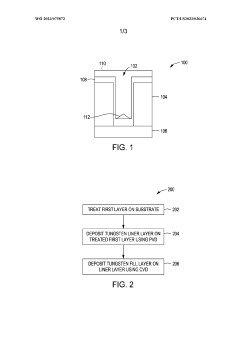
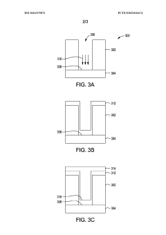
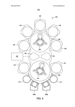
- The proposed method involves a physical vapor deposition of a tungsten liner, followed by an atomic layer deposition nucleation layer and a chemical vapor deposition bulk fill process, with a nitridation step and optional rapid thermal processing to reduce internal stresses and lower resistivity, using argon or krypton as ambient gases and optimizing temperature, pressure, and nitridation conditions.
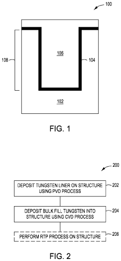
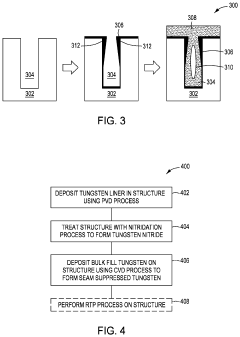
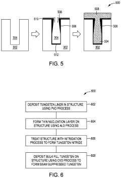
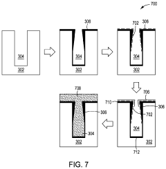
- A method involving a pre-deposition surface treatment to modify the PVD W liner properties, followed by a CVD W fill process, which reduces PVD W liner resistivity and incubation delay, thereby improving contact resistance and eliminating voids by using a PVD W liner in conjunction with a CVD W fill, specifically employing treatments like B2H6 WFe nucleation or CCTBA soak processes.
Environmental Impact of Tungsten Semiconductor Manufacturing
The environmental impact of tungsten semiconductor manufacturing is a critical consideration as the industry advances towards new frontiers. Tungsten's unique properties make it an attractive material for semiconductor applications, but its extraction and processing pose significant environmental challenges.
Mining and extraction of tungsten ore often involve open-pit mining, which can lead to habitat destruction, soil erosion, and water pollution. The process requires substantial energy inputs and may release harmful pollutants into the air and water. Additionally, tungsten mining often occurs in ecologically sensitive areas, further exacerbating its environmental footprint.
The refining and purification of tungsten for semiconductor-grade materials involve complex chemical processes. These processes generate hazardous waste products, including acidic solutions and heavy metal contaminants. Proper disposal and treatment of these wastes are essential to prevent environmental contamination and protect human health.
Semiconductor manufacturing using tungsten also consumes significant amounts of water and energy. The high-temperature processes required for tungsten deposition and etching contribute to increased energy consumption and greenhouse gas emissions. Water usage in cleaning and cooling processes can strain local water resources, particularly in water-scarce regions.
However, the industry is making strides in mitigating these environmental impacts. Advanced recycling technologies are being developed to recover and reuse tungsten from manufacturing waste and end-of-life products. This not only reduces the demand for raw tungsten but also minimizes waste generation.
Manufacturers are also implementing more efficient production processes to reduce energy consumption and emissions. This includes the adoption of advanced process control systems, optimization of equipment usage, and the integration of renewable energy sources in manufacturing facilities.
Water conservation efforts are gaining traction, with companies implementing closed-loop water systems and advanced water treatment technologies. These initiatives aim to reduce freshwater consumption and minimize the discharge of contaminated wastewater.
As the demand for tungsten in semiconductor applications grows, there is an increasing focus on developing more sustainable sourcing practices. This includes exploring alternative tungsten sources, such as recycled materials, and working with suppliers to ensure responsible mining practices.
The semiconductor industry is also investing in research to develop alternative materials that could potentially replace tungsten in certain applications, thereby reducing the overall environmental impact associated with tungsten extraction and processing.
Tungsten Semiconductor Integration Strategies
Tungsten semiconductor integration strategies have emerged as a critical focus in advancing semiconductor technology. The integration of tungsten into semiconductor devices offers several advantages, including improved electrical conductivity, enhanced thermal stability, and reduced resistance in interconnects. One key strategy involves the development of advanced deposition techniques for tungsten thin films. Chemical Vapor Deposition (CVD) and Atomic Layer Deposition (ALD) have been refined to achieve precise control over film thickness and uniformity, crucial for creating high-performance transistor gates and interconnects.
Another significant integration strategy is the optimization of tungsten's interface with other materials in the semiconductor stack. This includes developing novel barrier layers to prevent tungsten diffusion into surrounding materials and improving adhesion between tungsten and dielectric layers. Researchers are exploring various material combinations and deposition sequences to minimize interfacial resistance and enhance overall device performance.
The miniaturization of semiconductor devices has led to the exploration of tungsten nanostructures. Integration strategies now include the fabrication of tungsten nanowires and nanotubes for use in advanced transistor architectures. These nanostructures offer potential solutions for reducing short-channel effects and improving carrier mobility in next-generation devices.
Selective deposition of tungsten is another frontier in integration strategies. This approach allows for the precise placement of tungsten in specific areas of the device structure without the need for subsequent etching steps. Selective deposition techniques are being developed to reduce process complexity and improve device yield, particularly in the formation of self-aligned contacts and vias.
The integration of tungsten in 3D semiconductor architectures presents both challenges and opportunities. Strategies are being developed to incorporate tungsten in through-silicon vias (TSVs) and in the fabrication of vertical transistors. These 3D integration techniques aim to increase device density and improve overall chip performance.
Researchers are also focusing on mitigating the challenges associated with tungsten integration, such as stress-induced defects and resistivity increases at small dimensions. Advanced annealing techniques and the incorporation of dopants are being explored to optimize tungsten's electrical and mechanical properties in nanoscale devices.
As the semiconductor industry moves towards more complex and heterogeneous integration, tungsten's role in system-in-package (SiP) and chiplet technologies is gaining attention. Integration strategies are being developed to leverage tungsten's properties in advanced packaging solutions, including its use in redistribution layers and as a thermal management material.