
A realization method of self-erasable fpga configuration module
A technology for configuration modules and implementation methods, applied in information storage, static memory, instruments, etc., can solve the problems that the digital system cannot be completed by itself, FPGA and PROM cannot work, and cannot provide protection, etc. The implementation method is simple, convenient, and guaranteed Normal work, avoiding the effect of accidental erase operation
Patent Information
- Authority / Receiving Office
- CN · China
- Patent Type
- Patents(China)
- Current Assignee / Owner
- Publication Date
- 2016-05-04
Smart Images
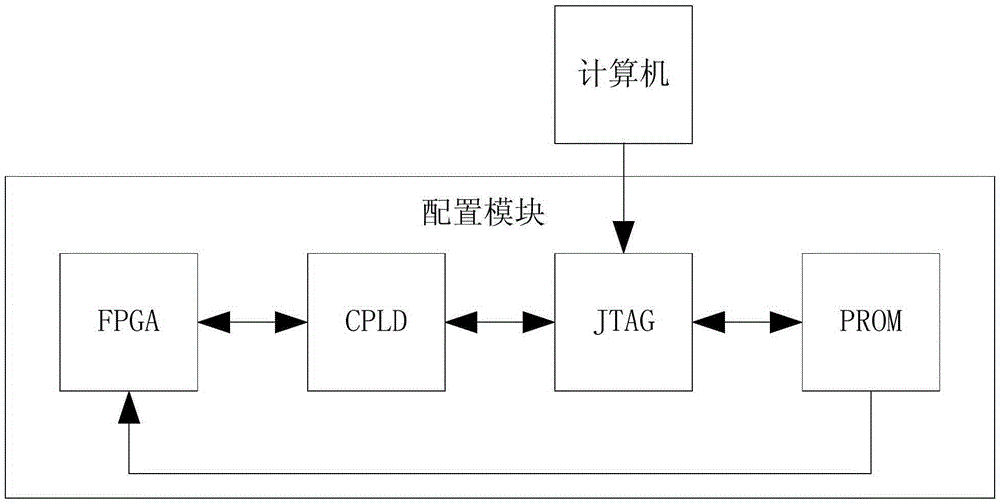
Figure 1 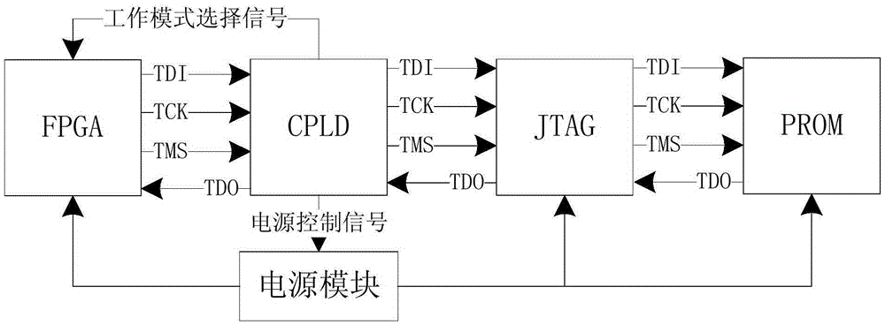
Figure 2 
Figure 3
Abstract
Description
technical field
[0001] The invention relates to a method for realizing a self-erasable FPGA configuration module, which belongs to the technical field of electronic products. Background technique
[0002] Existing methods for erasing the FPGA configuration information stored on the PROM include a software erasing method and a physical destruction method.
[0003] The software erasing method is to use the software provided by FPGA and PROM design manufacturers to erase. Taking Xilinx products as an example, the IMPACT software provided by this manufacturer can complete the erasing operation of configuration information, but this method must rely on the computer And the corresponding software to complete, the digital system cannot complete by itself, so there are certain limitations.
[0004] The method of physical destruction usually adopts the method of electric burning, so that FPGA and PROM cannot work. However, it has been proved by experiments that electric burning onl...
Examples
Embodiment Construction
[0035] Below in conjunction with accompanying drawing and specific embodiment the present invention is described in further detail:
[0036] In order to meet the requirements of technical confidentiality, the digital system needs to erase the configuration information of the FPGA to avoid obtaining relevant technical information through the configuration information. For digital systems designed based on FPGA and PROM, due to the storage characteristics of FPGA, the configuration information on it will be lost after power off, so it is only necessary to erase the configuration information on the PROM. The access, programming and erasing of PROM can be realized through JTAG. The present invention designs a self-erasable FPGA configuration module, which simulates JTAG to issue erasing instructions to the PROM by generating relevant signals through the FPGA, thereby completing the self-erasing operation.
[0037] Such as figure 1 Shown is the schematic diagram of the FPGA confi...