Supercharge Your Innovation With Domain-Expert AI Agents!

Capacitive touch circuit pattern and manufacturing method thereof

a manufacturing method and touch circuit technology, applied in the direction of electronic switching, pulse technique, instruments, etc., can solve the problems of difficult to effectively reduce the impedance between the electrode block and the surrounding circuit, and the overall process is very complex, so as to simplify the process of disposing the touch circuit pattern

Active Publication Date: 2019-05-07
TPK TOUCH SOLUTIONS (XIAMEN) INC
View PDF131 Cites 0 Cited by
  • Summary
  • Abstract
  • Description
  • Claims
  • Application Information

AI Technical Summary

Benefits of technology

[0006]An object of the present disclosure is to provide a capacitive touch circuit pattern and a manufacturing method for completing formation of electrode blocks along two axial directions together through a single process so as to simplify the process of disposing the touch circuit pattern.
[0075]Plurality of first-axis and second-axis electrode blocks of the present disclosure can be formed through a single process, which can simplify the process of disposing the touch circuit pattern.

Problems solved by technology

The shortcoming in this procedure is that for making the electrode blocks of the two groups of the capacitive sensing layers, the insulation layer and the two groups of surrounding circuits must be formed through the above disclosed five processing steps, which makes the overall process very complex.
Conductive wires used for connecting the electrode blocks are made of ITO, which further makes it difficult to effectively reduce the impedance between the electrode blocks and the surrounding circuits.

Method used


Image

  • Capacitive touch circuit pattern and manufacturing method thereof
  • Capacitive touch circuit pattern and manufacturing method thereof
  • Capacitive touch circuit pattern and manufacturing method thereof

Examples


Embodiment Construction

[0081]Detailed description of the present disclosure will be combined with the drawings.

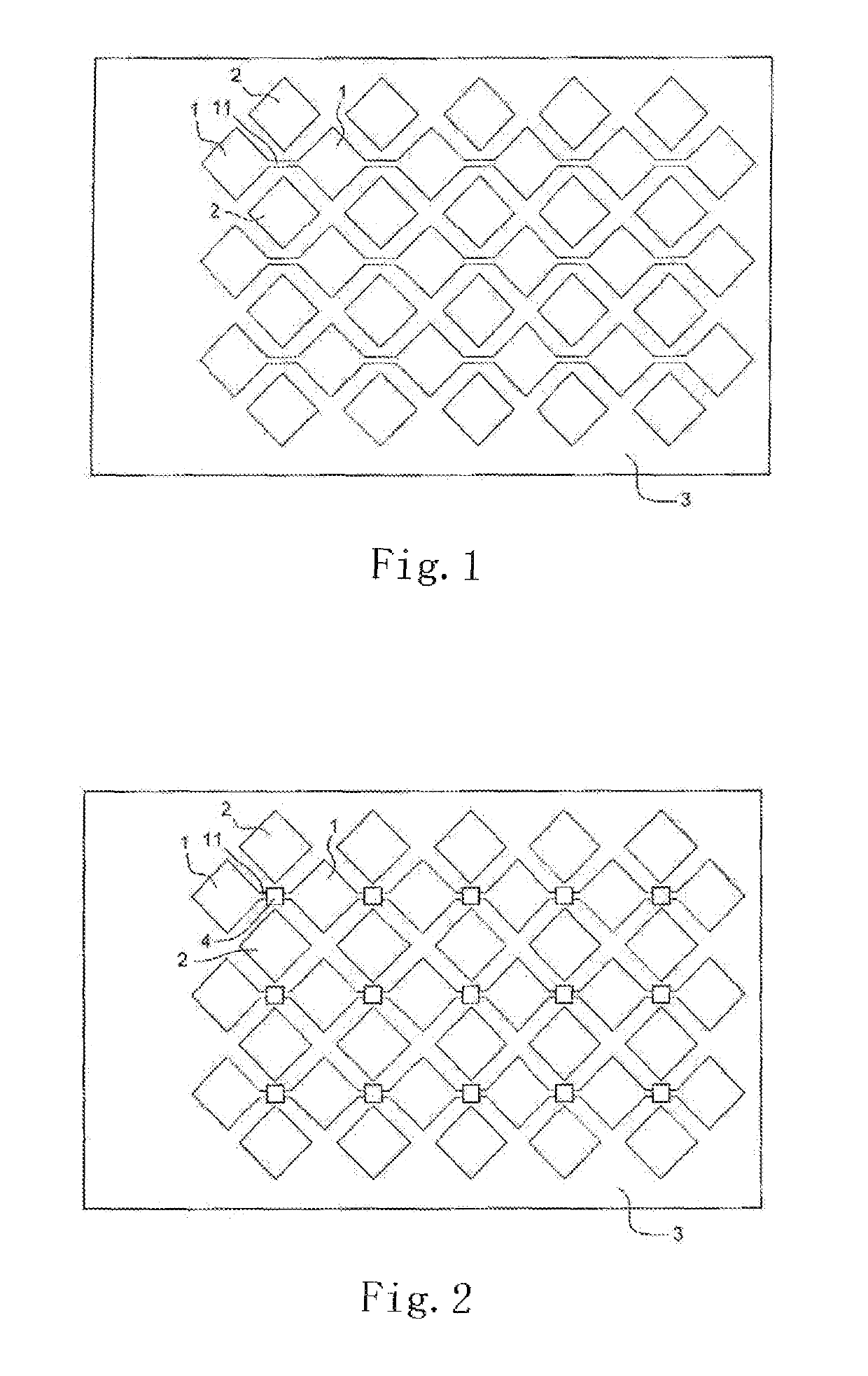
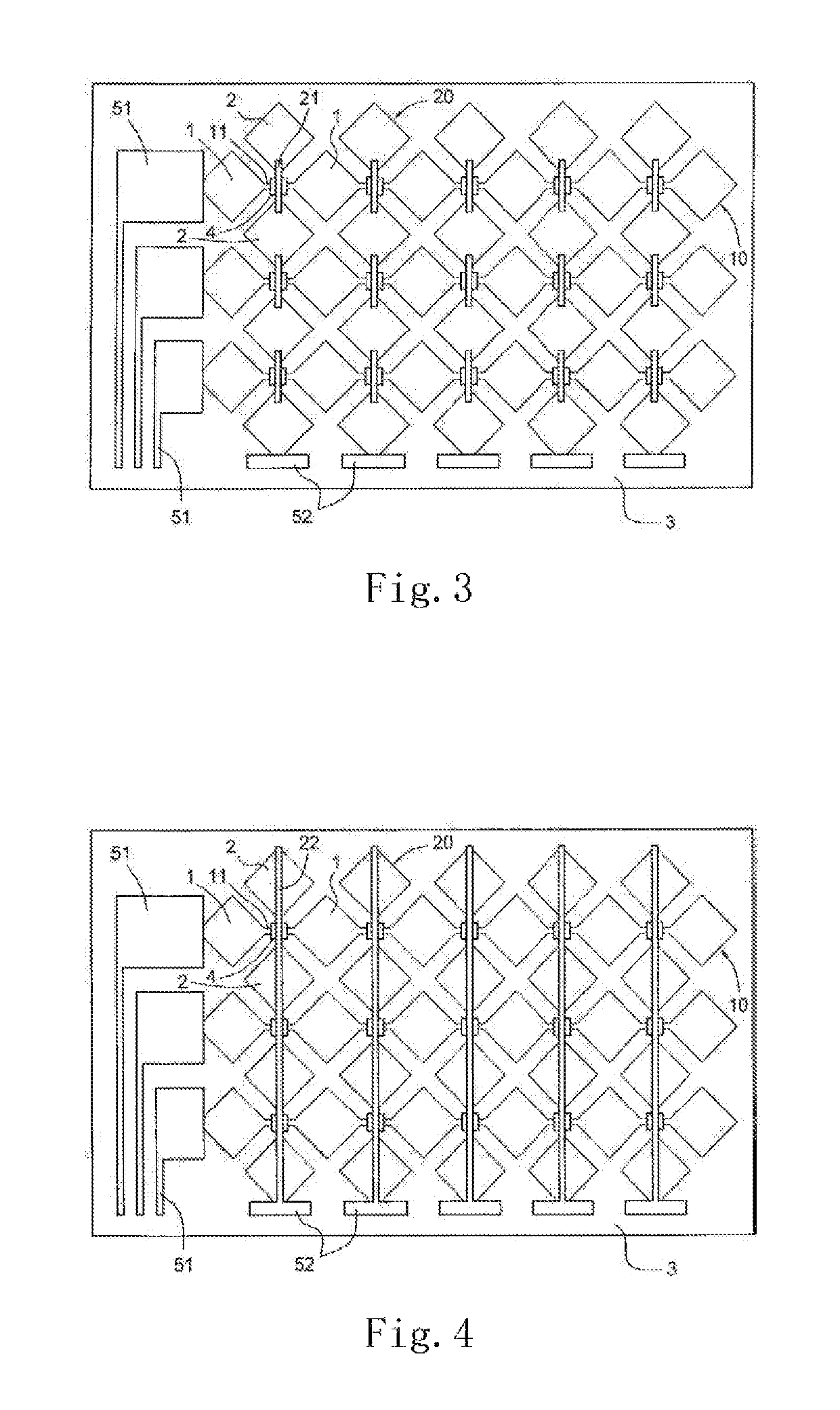
[0082]Illustratively, FIG. 3 discloses a plan view of a capacitive touch circuit pattern in accordance with the present disclosure and combining with FIG. 1 and FIG. 2, it can be seen that the present disclosure forms at least two adjacent transparent first-axis electrode blocks 1, a transparent first-axis conductive wire 11, and at least two adjacent transparent second-axis electrode blocks 2 on the surface of a substrate 3. The first-axis conductive wire 11 is formed between the two adjacent first-axis electrode blocks 1 to connect the two adjacent first-axis electrode blocks 1. The two adjacent second-axis electrode blocks 2 are disposed, respectively, at two sides of the first-axis conductive wire 11, and a second-axis conductive wire 21, which is Made of a metal material, connects the two adjacent second-axis electrode blocks 2 and stretches across the first-axis conductive wire 11. An insul...


PUM

PropertyMeasurementUnit
transparentaaaaaaaaaa
conductiveaaaaaaaaaa
non-transparent conductiveaaaaaaaaaa

Abstract

The present disclosure relates to a touch circuit pattern and a manufacturing method thereof. A capacitive touch circuit pattern in the present disclosure comprises a substrate, wherein at least two adjacent transparent first-axis electrode blocks, a transparent first-axis conductive wire, and at least two adjacent transparent second-axis electrode blocks are formed on the substrate. The first-axis conductive wire is formed between the two adjacent first-axis electrode blocks to connect the two adjacent first-axis electrode blocks and the two adjacent second-axis electrode blocks, respectively, at two sides of the first-axis conductive wire. The capacitive touch circuit pattern further comprises of a metal second-axis conductive wire, which stretches across the first-axis conductive wire and connects the two adjacent second-axis electrode blocks.

Description

FIELD OF THE INVENTION[0001]The present disclosure relates to a touch circuit pattern and a manufacturing method thereof, and more particularly to a capacitive touch circuit pattern formed on surface of a transparent substrate and a disposition technology thereof.BACKGROUND OF THE INVENTION[0002]Conventional touch input modes of touch panels comprise of resistive mode, capacitive mode, optical mode, electromagnetic induction mode, and acoustic wave sensing mode, etc. For the resistive mode and capacitive mode, a user touches the surface of a panel by a finger or a stylus, causing a change of voltage and current inside touch location of the panel, and then the touch location on surface of the panel can be detected so to achieve the purpose of a touch input.[0003]In order to detect a location on a touch panel touched by a user with a finger or a stylus, those skilled in the art have developed various capacitive touch sensing technologies. For example, structure of a grid capacitive to...

Claims


Application Information

Patent Timeline
Patent Type & Authority Patents(United States)
IPC IPC(8): G06F3/044
CPCG06F3/044Y10T29/49105G06F2203/04111G06F3/0443G06F3/0446G06F3/0412G06F2203/04103G06F3/0448
Inventor LIU, CHEN-YUWANG, CHING-YI
Owner TPK TOUCH SOLUTIONS (XIAMEN) INC
Features
  • R&D
  • Intellectual Property
  • Life Sciences
  • Materials
  • Tech Scout
  • Unparalleled Data Quality
  • Higher Quality Content
  • 60% Fewer Hallucinations
Learn More